
Bi-layer hole-injecting layer composed of molybdenum oxide and polyelectrolyte for solution-processed OLEDs with prolonged stability†
Jinghong Peng,
Xinjun Xu*,
Chuang Yao and
Lidong Li*
State Key Lab for Advanced Metals and Materials, School of Materials Science and Engineering, University of Science and Technology Beijing, Beijing 100083, China. E-mail: xuxj@mater.ustb.edu.cn; lidong@mater.ustb.edu.cn
First published on 10th October 2016
Abstract
Currently, poly(3,4-ethylene-dioxythiophene):poly(styrene sulfonic acid) (PEDOT:PSS) is predominantly used as the hole-injecting layer in solution processed organic light-emitting diodes (OLEDs). However, its strong acidity is detrimental to device stability. Here, a bi-layer hole-injecting layer (BHIL) composed of molybdenum trioxide (MoO3) and an anionic polyelectrolyte has been used in solution processed OLEDs to replace PEDOT:PSS. The MoO3 layer was firstly solution deposited using low temperature combustion processing, which ensured that the device had a good hole-transporting ability. Then, an anionic polyelectrolyte was deposited on to the MoO3 layer also using a solution process, resulting in work function increase which was verified using peak force Kelvin probe force microscopy. Thus, the hole-injecting ability of the BHIL was found to be enhanced. It was found that BHIL-based OLEDs possessed a comparable electroluminescence performance but a better shelf-stability relative to the PEDOT:PSS based devices. This strategy gives a promising approach to obtaining high performance solution processed OLEDs with long-term stability.
Introduction
Organic light-emitting diodes (OLED) have been attracting considerable attention from researchers because they hold promise for applications in the flat panel display and solid-state lighting fields.1–4 In order to meet the requirements of optical and electrical performance for commercial application, tremendous efforts have been made to optimize the electroluminescence (EL) efficiency and stability of the OLED devices.5–10One of the most important factors for achieving an efficient and stable device is the selection and fabrication of the functional buffer layer between the electrodes and organic semiconductor film, which can facilitate the injecting and transporting of holes or electrons.11–13 Utilizing a proper hole-injecting layer (HIL) as the anode buffer layer can not only decrease the energy barrier for the hole injecting from indium tin oxide (ITO) to the hole-transporting layer (HTL) or emissive layer (EML), but also provides a smoother interface to reduce the current leakage.14 Because solution processing is energy and time efficient and it can be compatible with the manufacturing of large sized devices, OLEDs fabricated by solution processing have more potential for practical uses than their thermal evaporation counterpart.15–17
Currently, the most commonly-used HIL material in solution processed OLEDs is poly(3,4-ethylene-dioxythiophene):poly(styrene sulfonic acid) (PEDOT:PSS), which possesses a favourable performance such as enough transparency in the visible region, high conductivity, relatively high work function and good film forming ability.18,19 However, because of the intrinsic high acidity of PEDOT:PSS, it can cause corrosion of the ITO anode and the EML. Also, the hygroscopic property of the PEDOT:PSS might cause it to migrate to attack the cathode of the device. Thus, it would degrade the device efficiency and long-term stability of OLEDs.20,21 To solve this problem, crosslinkable organic hole-injecting or hole-transporting materials have been developed.22,23 Nevertheless, these crosslinkable materials suffer from the following disadvantages: (1) the residual crosslinkable groups in molecules are detrimental to the charge transport; (2) they usually need a high crosslinking temperature (>150 °C) which is incompatible with the flexible plastic substrates for future roll-to-roll manufacturing;24,25 some of them have a low surface energy, so it is hard to wet them during the solution deposition of the upper layer and only vacuum thermal evaporation is suitable for deposition of the subsequent EML.26 As a result, developing appropriate HIL for solution processed OLEDs is still highly desirable.
Besides organic HILs, transition metal oxides, such as vanadium oxide (VOx),27,28 nickel oxide (NiO),29 tungsten oxide (WO3),30 and molybdenum oxide (MoOx)31–36 have usually been utilized as anode buffer layers in organic optoelectronic devices, especially in organic photovoltaic cells (OPVs). Among them, molybdenum trioxide (MoO3) has been widely used because it has advantages such as high transmittance, less contamination, and good charge transporting ability.31–33 It has been reported that a solution processed MoO3 hole selective layer was fabricated in an OPV device using low temperature combustion processing.31 This MoO3-based device has obtained comparable power conversion efficiency and better shelf-stability with the PEDOT:PSS device. It should be noted that good shelf-stability is a critical factor for the long-term stability of organic optoelectronic devices. Currently, there are only a few studies about selecting and utilizing suitable functional film layers to improve the shelf-stability of organic optoelectronic devices.37 In contrast to OPV devices, in OLEDs holes are injected and transported from the anode buffer layer to the organic active layer, which was the opposite direction to that of OPVs. As a consequence of the energy level mismatch, this solution processed MoO3 film might not be suitable to be used as the HIL in OLEDs. Considering that cationic polyelectrolytes have been used as a universal method to produce low work function electrodes for organic electronics,38 it might be practical to use an anionic polyelectrolyte to increase the work function of the HIL in OLEDs. Thus, the modified HIL can be expected to decrease the energy barrier between the ITO anode and the EML, offering an alternative to conventional PEDOT:PSS HIL in solution processed OLEDs.
In this study, bi-layer hole-injecting layer (BHIL) were fabricated and then used in solution processed OLEDs comprising MoO3 and an anionic polyelectrolyte. The MoO3 thin film layer was first deposited using low temperature combustion processing, which ensured good hole-transporting ability for the device. Then, an anionic polyelectrolyte, poly(sodium 4-styrenesulfonate) (PSS-Na), was deposited on MoO3 using solution processing. The PSS-Na can form suitable dipoles at the interface, which can increase the work function of MoO3 and thus enhance the hole-injecting ability in the BHIL-based devices. It was found that the BHIL-based OLEDs possessed comparable EL performance but better shelf-stability compared to the PEDOT:PSS-based ones.
Experimental
Materials
PEDOT:PSS (Clevios™ PVP Al 4083) was purchased from H. C. Starck Clevios GmbH. Ammonium heptamolybdate [(NH4)6Mo7O24·4H2O, AHM], PSS-Na (MW ∼ 70![[thin space (1/6-em)]](https://www.rsc.org/images/entities/char_2009.gif) 000), acetylacetone, and poly(9-vinylcarbazole) (PVK, MW ∼ 1100000) were purchased from Sigma-Aldrich. 1,3-Bis[(4-tert-butylphenyl)-1,3,4-oxadiazolyl]phenylene (OXD-7) and iridium(III) bis[(4,6-fluorophenyl)-pyridinato-N,C2′]picolinate (FIrpic) were purchased from Nichem Fine Technology Co. Ltd. Other chemicals were obtained from J&K Chemical Ltd. All the reagents were used as received.
000), acetylacetone, and poly(9-vinylcarbazole) (PVK, MW ∼ 1100000) were purchased from Sigma-Aldrich. 1,3-Bis[(4-tert-butylphenyl)-1,3,4-oxadiazolyl]phenylene (OXD-7) and iridium(III) bis[(4,6-fluorophenyl)-pyridinato-N,C2′]picolinate (FIrpic) were purchased from Nichem Fine Technology Co. Ltd. Other chemicals were obtained from J&K Chemical Ltd. All the reagents were used as received.
Deposition of MoO3 thin film
The MoO3 thin film layer was deposited using low temperature combustion processing, according to a previous method.31 Briefly, 285 μL of acetylacetone was dropped into 5 mL of the AHM aqueous solution (0.01 M). Then, 605 μL of concentrated nitric acid (65%) was added, followed by the addition of a small amount of PEDOT:PSS solution (29 μL) to improve the film forming ability. The mixture was continually stirred at 1500 rpm during the preparation. After stirring for 10 min, the solution was filtered through a 0.45 μm poly(vinylidene fluoride) filter. Then, a 10 nm MoO3 film was formed by spin-coating the solution on to the ITO substrate at 4000 rpm for 40 s followed by thermal annealing at 150 °C for 10 min in an ambient environment.Fabrication of OLEDs
OLEDs were fabricated on patterned ITO-coated glass substrates with a sheet resistance of 10 Ω sq−1 purchased from CSG Holding Co. Ltd. The ITO-coated glass substrates were cleaned with detergent, then sequentially ultrasonicated in deionized water (H2O), acetone, and alcohol followed by ultraviolet-ozone treatment for 6 min. The BHIL-based OLED was in a device configuration of ITO/BHIL (MoO3/PSS-Na)/EML/Ca/Al. The MoO3 layer was first deposited on the pre-dispersed ITO substrates as described previously. Then a ∼10 nm PSS-Na layer was spin-coated from its H2O/methanol (1:1, v/v) solution (2 mg mL−1) and baked at 100 °C for 20 min. After that, a solution containing a mixture of PVK:OXD-7:FIrpic (10:4:1 weight ratio) in a total concentration of 15 mg mL−1 was spin-coated onto the BHIL layer and baked at 100 °C for 30 min to form an 80 nm EML. The depositing and annealing of the EML was in a nitrogen filled glovebox (H2O < 0.1 ppm, O2 < 0.1 ppm). Finally, calcium (Ca; 6 nm) and aluminium (Al; 100 nm) were deposited sequentially using thermal evaporation onto the EML under a vacuum of 5 × 10⁻⁴ Pa, to act as the cathode. The active area of each device was 0.04 cm2, defined by the overlap of electrodes. Also, OLEDs with a HIL of 40 nm PEDOT:PSS and a HIL consisting of a single MoO3 layer were also fabricated as the reference devices.
Characterization
The film thickness was measured using an Ambios Technology XP2 profilometer. The work function value was measured using peak force Kelvin probe force microscopy (PF-KPFM) mode on a Bruker MultiMode 8 microscope, and Bruker PFQNE-AL probes were used for the measurement. Gold (Au) film (500 nm) was deposited using thermal evaporation for reference in the PF-KPFM measurements. The surface morphology of each film was measured using atomic force microscopy (AFM, Bruker Multimode 8). The EL spectra were recorded on an Ocean Optics Maya2000Pro spectrophotometer. The current density–luminance–voltage (J–L–V), luminous efficiency–current density (η–J), and external quantum efficiency (EQE)–current density (EQE–J) characteristics were measured in a nitrogen filled glovebox with a Keithley 2612B source measurement unit and a silicon photodiode calibrated using a PR-655 SpectraScan spectroradiometer.Results and discussion
As shown in Fig. 1, the device structure of the BHIL-based OLED used in this study was ITO/BHIL (MoO3/PSS-Na)/PVK:OXD-7:FIrpic (10:4:1 weight ratio)/Ca/Al. The BHIL of the device was composed of a MoO3 thin film and a PSS-Na layer, which was deposited as described in the Experimental section. PVK was utilized as the host material, and OXD-7 was incorporated into the PVK host to facilitate the electron-transporting property in the EML. FIrpic was doped into the EML to serve as the sky-blue phosphorescence emitter. The molecular structures of the relevant materials are also shown in Fig. 1.
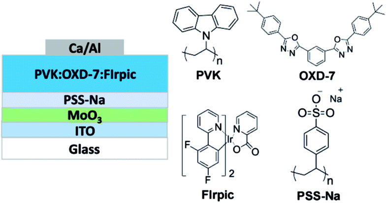 | ||
| Fig. 1 Device structure of the BHIL-based OLED and molecular structures of the relevant materials. | ||
To investigate the hole-transporting properties of a BHIL-based device, hole-only devices with a structure of ITO/HIL/EML (80 nm)/Au (100 nm) were fabricated. As well as the BHIL, hole-only devices using single-layer MoO3, single-layer PSS-Na, and PEDOT:PSS as the HIL were also fabricated as reference materials. Fig. 2 shows the current density–electric field characteristics of these hole-only devices. It can be seen that the device with the MoO3/PSS-Na BHIL showed the highest hole current density of all these devices. Compared with the device using single PSS-Na as HIL, the higher hole current density in the BHIL device indicated that incorporation of the MoO3 layer could improve the hole-transporting ability of the device. It is also obvious that the hole current density of the BHIL device was a little higher than that in the PEDOT:PSS device. Also, compared with the device containing a single MoO3 layer, the higher hole current density in the BHIL-based device might originate from the reduced energy barrier between MoO3 and EML after incorporating the anionic polyelectrolyte PSS-Na.
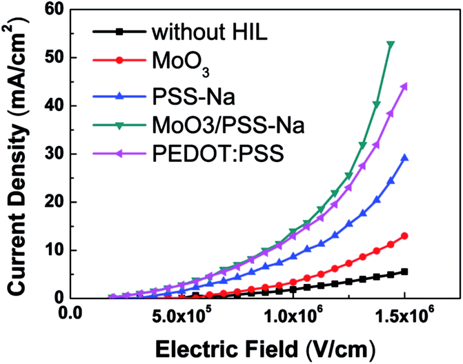 | ||
| Fig. 2 Current density–electric field characteristics of the hole-only devices with different HILs. | ||
In order to verify the effect of incorporating anionic polyelectrolyte PSS-Na, PF-KPFM measurements was carried out to investigate the work function of a single MoO3 layer and MoO3/PSS-Na bi-layer on ITO. The PF-KPFM images (Fig. S1; ESI†) showed that the relative contact potential difference distributions of the single MoO3 layer and MoO3/PSS-Na bi-layer were relatively homogeneous. It was revealed that the surface work function of a single MoO3 layer and a MoO3/PSS-Na bi-layer were 5.3 and 5.6 eV, respectively. This could explain the J–V characteristics of the hole-only devices shown in Fig. 2. As illustrated in Fig. 3, work function increase was 0.3 eV by incorporating the PSS-Na layer. The increase of work function has reduced the energy barrier when the holes were injected from MoO3 to the highest occupied molecular orbital of PVK. This could contribute to obtaining efficient and stable devices.
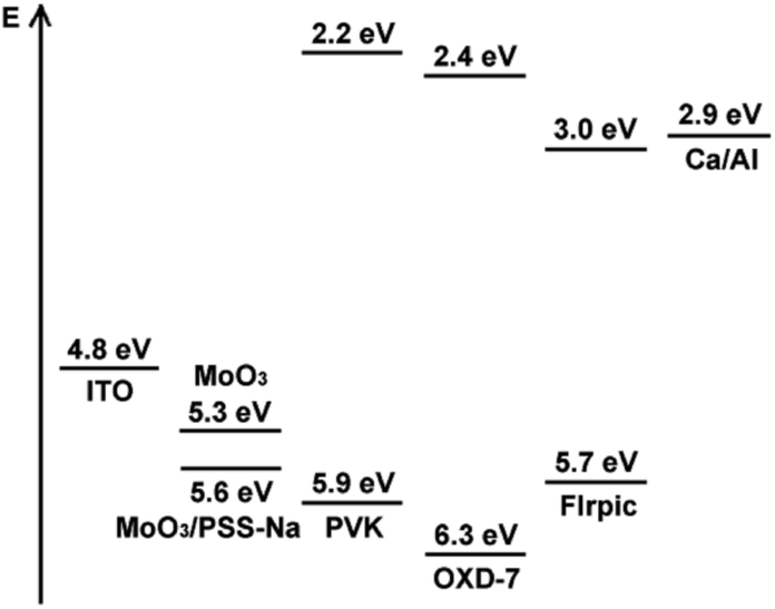 | ||
| Fig. 3 Energy level diagram of materials used in this study. | ||
To confirm that the surface morphology of films is crucial for device performance, AFM measurements were utilized to investigate the film forming properties of the HILs. The HIL films were deposited under the same conditions as the OLED devices. Fig. 4 shows the AFM images of the ITO/MoO3 and ITO/MoO3/PSS-Na substrates, with root-mean-square roughness (Rq) values of 2.09 nm and 1.59 nm, respectively. The Rq of the MoO3/PSS-Na BHIL was greatly improved compared with the bare ITO (2.42 nm), which was even comparable with that of the commonly-used HIL PEDOT:PSS (1.36 nm) (shown in Fig. S2; ESI†). This indicated that the depositing of the PSS-Na layer has helped to smooth the surface of MoO3, in favor of the subsequent film forming of the organic emissive layer. The smoother surface and better film forming ability of organic film could also reduce the current leakage and thus improve the performance of the device.39
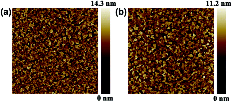 | ||
| Fig. 4 AFM images (5 μm × 5 μm scale) of the (a) ITO/MoO3 and (b) ITO/MoO3/PSS-Na substrates. | ||
The J–L–V and η–J characteristics of the devices based on MoO3/PSS-Na BHIL and PEDOT:PSS HIL are shown in Fig. 5, and the EL performance of the devices (including the device with a single MoO3 HIL, shown in Fig. S3; ESI†) are summarized in Table 1. In Fig. 5a, the BHIL-based device showed similar current density to that of the PEDOT:PSS-based device at low driving voltages. When the voltage was higher, the current density of the BHIL-based device became higher than that of the PEDOT:PSS-based device, indicating that the incorporation of MoO3/PSS-Na BHIL could produce a positive effect on the hole injecting and transporting abilities of the device. The poor performance of the device based on a single MoO3 HIL (Fig. S3; ESI†) could be caused by the relatively high energy barrier for the hole injection. As can be seen in Fig. 5a, the maximum luminance of the BHIL-based device (26213 cd m−2) was also higher than that of the PEDOT:PSS-based device (21189 cd m−2). The BHIL-based device also showed a comparable turn-on voltage, maximum luminous efficiency, and maximum EQE (5.8 V, 15.09 cd A−1, and 6.50%, respectively) with those of the PEDOT:PSS-based device (5.6 V, 14.51 cd A−1, and 6.74%, respectively). The EQE–J characteristics are shown in Fig. S4 (ESI†). The PEDOT:PSS-based device showed a little lower current density than the BHIL-based device when the luminous efficiency was increased. As the maximum luminous efficiency was reached, the two devices showed nearly the same current density (Fig. S5; ESI†). Also, the slightly higher turn-on voltage of the BHIL-based device than that of the PEDOT:PSS-based device might be caused by the difference in the HIL's conductivity. As shown in Fig. 2, when the driving electric field was lower, the PEDOT:PSS-based device showed comparable or even a little higher hole current density. This could result in the slightly lower turn-on voltage of the PEDOT:PSS-based device. In Fig. 5c, it is obvious that both of the devices show almost identical EL spectra. The emission peaks located at 475 and 500 nm originated from the emission of FIrpic.40 Therefore, the BHIL-based device had a comparable EL performance to the PEDOT:PSS-based device.
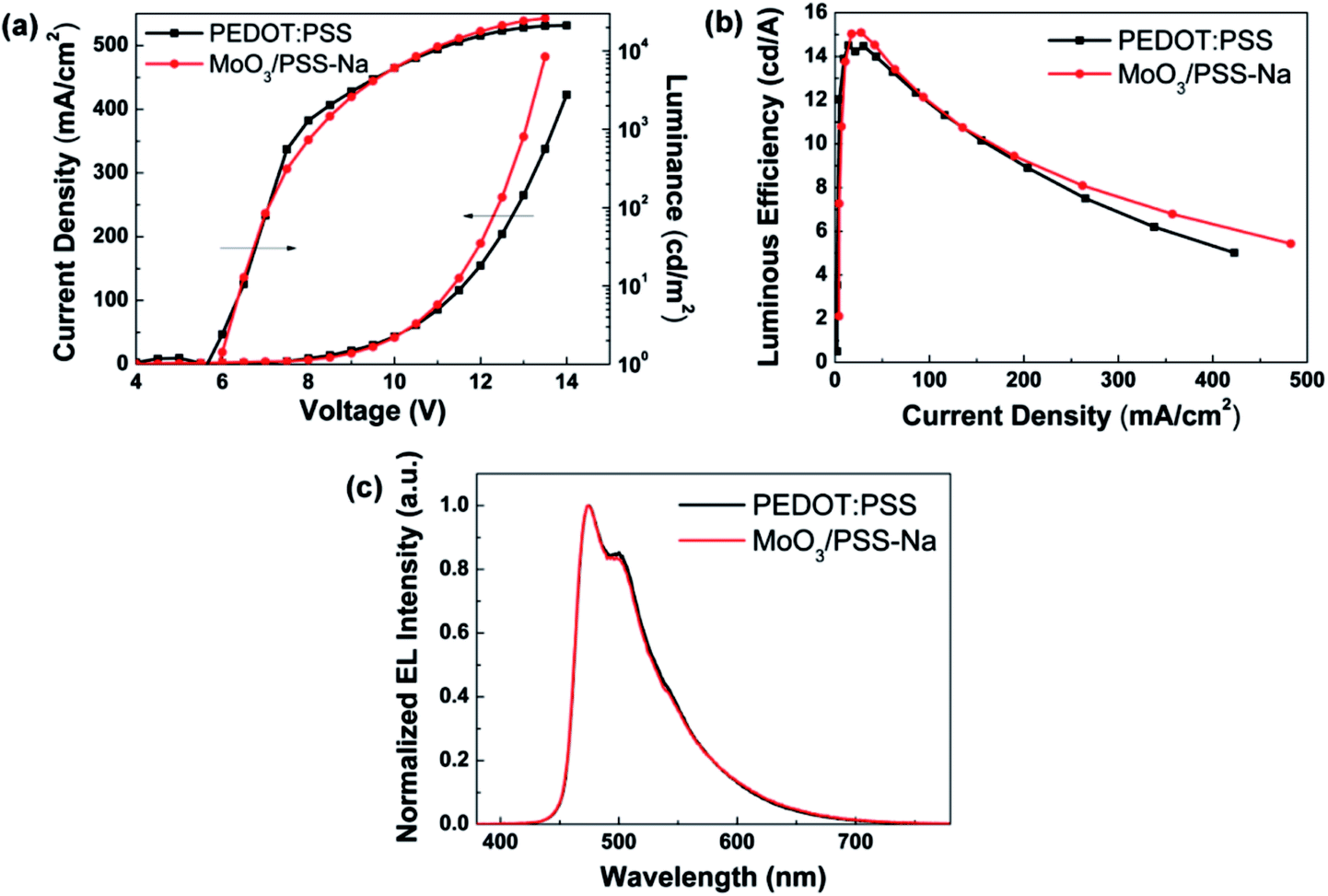 | ||
| Fig. 5 (a) J–L–V characteristics, (b) η–J characteristics and (c) normalized EL spectra of devices based on MoO3/PSS-Na BHIL and PEDOT:PSS HIL. | ||
The thickness effect of the PSS-Na layer has also been investigated. The EL performance of devices based on BHIL with a PSS-Na thickness of 5 nm and 20 nm is shown in Fig. S6 (ESI†). The device based on a thinner (5 nm) PSS-Na layer showed poor EL performance with a turn-on voltage of 10.9 V, a maximum luminance of 1527 cd m−2, and a maximum luminous efficiency of 3.56 cd A−1. This might be ascribed to the incomplete coverage of PSS-Na on the MoO3 layer and thus the energy barrier of hole injection was high. The device based on a thicker PSS-Na (20 nm) layer also showed a higher turn-on voltage (10.8 V), lower maximum luminance (11295 cd m−2), and lower maximum luminous efficiency (10.38 cd A−1) than the device based on a 10 nm thick PSS-Na layer. When the PSS-Na layer becomes thicker, the insulating nature of PSS-Na would have a negative effect on the device performance.38 Therefore, the PSS-Na layer thickness of ∼10 nm was suitable for obtaining a good EL performance of the device.
The investigation of the shelf-stabilities of OLEDs with different HILs is shown in Fig. 6. To exclude the effect of Ca cathode degradation,41 the measurement was conducted in a nitrogen atmosphere. As can be seen, the luminance of the PEDOT:PSS-based device decreased to less than 30% of the initial value after 600 h. Because of the intrinsic high acidity of the PEDOT:PSS, corrosion of the ITO anode degraded the device performance and long-term stability.20,21 Whereas the MoO3/PSS-Na BHIL-based device maintained over 90% of its initial luminance even after 960 h. The significantly prolonged shelf stability in the BHIL-based device was mainly attributed to the better compatibility of the ITO and MoO3 film. The results indicated that the BHIL-based device possessed a much better shelf-stability than the PEDOT:PSS-based device.
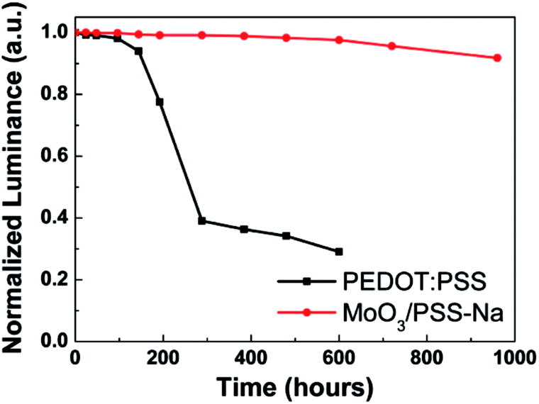 | ||
| Fig. 6 Normalized luminance for OLEDs with different HILs as a function of storage time in a nitrogen atmosphere. The measurement was at a current density of 7.9 mA cm−2 under an initial luminance of 1000 ± 100 cd m−2. | ||
Conclusions
In summary, a bi-layer hole-injecting layer (BHIL) has been incorporated in solution processed OLEDs. Among the BHIL used, the MoO3 thin film, which was solution deposited via low temperature combustion processing, ensured a good hole-transporting ability for the device. However, anionic polyelectrolyte PSS-Na, which was also deposited on the MoO3 layer by solution processing, increases the work function of MoO3 and thus enhances the hole-injecting ability of the BHIL. It was found that the BHIL-based OLED possessed comparable EL performance but significantly prolonged shelf-stability relative to the PEDOT:PSS-based device. These results are a promising approach to obtain high performance, solution processed OLEDs with long-term stability.Acknowledgements
This work is supported by the National Natural Science Foundation of China (51273020, 51373022), the State Key Laboratory for Advanced Metals and Materials (2016Z-08) and Research Fund for the Doctoral Program of Higher Education of China (20130006110007).Notes and references
- C. W. Tang and S. A. VanSlyke, Appl. Phys. Lett., 1987, 51, 913 CrossRef CAS.
- M. Pfeiffer, S. R. Forrest, K. Leo and M. E. Thompson, Adv. Mater., 2002, 14, 1633 CrossRef CAS.
- H. Wu, G. Zhou, J. Zou, C.-L. Ho, W.-Y. Wong, W. Yang, J. Peng and Y. Cao, Adv. Mater., 2009, 21, 4181 CrossRef CAS.
- Y. Tao, C. Yang and J. Qin, Chem. Soc. Rev., 2011, 40, 2943 RSC.
- C. C. Wu, C. I. Wu, J. C. Sturm and A. Kahn, Appl. Phys. Lett., 1997, 70, 1348 CrossRef CAS.
- S. Reineke, F. Lindner, G. Schwartz, N. Seidler, K. Walzer, B. Lussem and K. Leo, Nature, 2009, 459, 234 CrossRef CAS PubMed.
- H. Uoyama, K. Goushi, K. Shizu, H. Nomura and C. Adachi, Nature, 2012, 492, 234 CrossRef CAS PubMed.
- F. Tang, J. Peng, R. Liu, C. Yao, X. Xu and L. Li, RSC Adv., 2015, 5, 71419 RSC.
- R. C. Kwong, M. R. Nugent, L. Michalski, T. Ngo, K. Rajan, Y.-J. Tung, M. S. Weaver, T. X. Zhou, M. Hack, M. E. Thompson, S. R. Forrest and J. J. Brown, Appl. Phys. Lett., 2002, 81, 162 CrossRef CAS.
- S. L. Tao, Z. K. Peng, X. H. Zhang, P. F. Wang, C. S. Lee and S. T. Lee, Adv. Funct. Mater., 2005, 15, 1716 CrossRef CAS.
- C.-H. Ku, C.-H. Kuo, C.-Y. Chen, M.-K. Leung and K.-H. Hsieh, J. Mater. Chem., 2008, 18, 1296 RSC.
- Y. Tian, X. Xu, J. Wang, C. Yao and L. Li, ACS Appl. Mater. Interfaces, 2014, 6, 8631 CAS.
- J. Peng, F. Tang, X. Xu, M. Jia and L. Li, RSC Adv., 2016, 6, 38148 RSC.
- X. Gong, D. Moses, A. J. Heeger, S. Liu and A. K.-Y. Jen, Appl. Phys. Lett., 2003, 83, 183 CrossRef CAS.
- C. D. Müller, A. Falcou, N. Reckefuss, M. Rojahn, V. Wiederhirn, P. Rudati, H. Frohne, O. Nuyken, H. Becker and K. Meerholz, Nature, 2003, 421, 829 CrossRef PubMed.
- H. Zheng, Y. Zheng, N. Liu, N. Ai, Q. Wang, S. Wu, J. Zhou, D. Hu, S. Yu, S. Han, W. Xu, C. Luo, Y. Meng, Z. Jiang, Y. Chen, D. Li, F. Huang, J. Wang, J. Peng and Y. Cao, Nat. Commun., 2013, 4, 1971 Search PubMed.
- J. Peng, X. Xu, Y. Tian, J. Wang, F. Tang and L. Li, Appl. Phys. Lett., 2014, 105, 173301 CrossRef.
- G. Heywang and F. Jonas, Adv. Mater., 1992, 4, 116 CrossRef CAS.
- Q. Xu, J. Ouyang, Y. Yang, T. Ito and J. Kido, Appl. Phys. Lett., 2003, 83, 4695 CrossRef CAS.
- W. H. Kim, A. J. Mäkinen, N. Nikolov, R. Shashidhar, H. Kim and Z. H. Kafafi, Appl. Phys. Lett., 2002, 80, 3844 CrossRef CAS.
- S.-Y. Yu, J.-H. Chang, P.-S. Wang, C.-I. Wu and Y.-T. Tao, Langmuir, 2014, 30, 7369 CrossRef CAS PubMed.
- C. Zhong, C. Duan, F. Huang, H. Wu and Y. Cao, Chem. Mater., 2011, 23, 326 CrossRef CAS.
- C. A. Zuniga, S. Barlow and S. R. Marder, Chem. Mater., 2011, 23, 658 CrossRef CAS.
- B. Ma, F. Lauterwasser, L. Deng, C. S. Zonte, B. J. Kim, J. M. J. Fréchet, C. Borek and M. E. Thompson, Chem. Mater., 2007, 19, 4827 CrossRef CAS.
- Y.-J. Cheng, M. S. Liu, Y. Zhang, Y. Niu, F. Huang, J.-W. Ka, H.-L. Yip, Y. Tian and A. K. Y. Jen, Chem. Mater., 2008, 20, 413 CrossRef CAS.
- J. Li and T. J. Marks, Chem. Mater., 2008, 20, 4873 CrossRef CAS.
- C.-P. Chen, Y.-D. Chen and S.-C. Chuang, Adv. Mater., 2011, 23, 3859 CAS.
- W. Xu, Y. Liu, X. Huang, L. Jiang, Q. Li, X. Hu, F. Huang, X. Gong and Y. Cao, J. Mater. Chem. C, 2016, 4, 1953 RSC.
- I.-M. Chan, T.-Y. Hsu and F. C. Hong, Appl. Phys. Lett., 2002, 81, 1899 CrossRef CAS.
- F. Wang, X. Qiao, T. Xiong and D. Ma, J. Appl. Phys., 2009, 105, 084518 CrossRef.
- C. Yao, X. Xu, J. Wang, L. Shi and L. Li, ACS Appl. Mater. Interfaces, 2013, 5, 1100 CAS.
- S. Höfle, H. Do, E. Mankel, M. Pfaff, Z. Zhang, D. Bahro, T. Mayer, W. Jaegermann, D. Gerthsen, C. Feldmann, U. Lemmer and A. Colsmann, Org. Electron., 2013, 14, 1820 CrossRef.
- F. Wang, X. Qiao, T. Xiong and D. Ma, Org. Electron., 2008, 9, 985 CrossRef CAS.
- T. Shizuo, N. Koji and T. Yasunori, J. Phys. D: Appl. Phys., 1996, 29, 2750 CrossRef.
- F. Wang, X. Qiao, T. Xiong and D. Ma, Org. Electron., 2008, 9, 985 CrossRef CAS.
- S. Bhaumik and A. J. Pal, ACS Appl. Mater. Interfaces, 2014, 6, 11348 CAS.
- S. Park, W. M. Yun, L. H. Kim, S. Park, S. H. Kim and C. E. Park, Org. Electron., 2013, 14, 3385 CrossRef CAS.
- Y. Zhou, C. Fuentes-Hernandez, J. Shim, J. Meyer, A. J. Giordano, H. Li, P. Winget, T. Papadopoulos, H. Cheun, J. Kim, M. Fenoll, A. Dindar, W. Haske, E. Najafabadi, T. M. Khan, H. Sojoudi, S. Barlow, S. Graham, J.-L. Brédas, S. R. Marder, A. Kahn and B. Kippelen, Science, 2012, 336, 327 CrossRef CAS PubMed.
- K. S. Yook and J. Y. Lee, Adv. Mater., 2014, 26, 4218 CrossRef CAS PubMed.
- Y. Tian, J. Peng, X. Xu and L. Li, RSC Adv., 2015, 5, 98075 RSC.
- M. S. Weaver, L. A. Michalski, K. Rajan, M. A. Rothman, J. A. Silvernail, J. J. Brown, P. E. Burrows, G. L. Graff, M. E. Gross, P. M. Martin, M. Hall, E. Mast, C. Bonham, W. Bennett and M. Zumhoff, Appl. Phys. Lett., 2002, 81, 2929 CrossRef CAS.
Footnote |
| † Electronic supplementary information (ESI) available: PF-KPFM images, additional AFM images, and additional device performance characterizations. See DOI: 10.1039/c6ra21705b |
| This journal is © The Royal Society of Chemistry 2016 |