
Ab initio calculation of halide ligand passivation on PbSe quantum dot facets†
B. Wang*,
H. Xia,
Z. Zhang,
J. Yang,
R. Patterson,
S. Huang,
S. Shrestha and
G. Conibeer
Australian Centre for Advanced Photovoltaics, School of Photovoltaics and Renewable Energy Engineering, University of New South Wales, Sydney, NSW 2052, Australia. E-mail: wangbostc@hotmail.com
First published on 25th October 2016
Abstract
The passivation and charge compensation provided by inorganic halide ligands on low index facets of lead selenide (PbSe) nanocrystals has been studied using density functional theory to produce projected densities of states (PDOS), bond lengths and to perform Bader analysis. The calculations were made using a grid-based planar augmented wave code with a localized double zeta potential basis and the generalized gradient approximation. Surface energies of halide ligands bonded onto surface Pb atoms show trends that are consistent with the increased electronegativity of the species, with iodine having the lowest binding energy of the halides investigated. Different densities of iodine ligands lead to different levels of passivation with a continuous widening of the bandgap on particular facets for increasing levels of coverage. In particular, the (111) plane shows a clear recovery of surface layer back to bulk property and widening of bandgap when the ligands cover most Pb atoms on the surfaces. Additionally, a possible increase of carrier conductance along with the increase of ligand density has been found using Bader analysis. Relative increases in the conductance for large halide atoms stem from the measurable increases to electronic states near the top of the valence band in these p-type semiconductors. The passivation is observed to increase along with the s-type character of the electron density at the surface, suggesting that a higher degree of symmetry in the electron density accompanies the reduction in defect levels.
I. Introduction
Lead chalcogenide nanoparticles have been shown to perform excellently when applied as semiconducting nanoparticles in advanced devices. PbSe in particular is a promising material and has been investigated for applications in advanced solar cells, LEDs and optical sensors.1–3 Apart from the conventional advantages in optoelectronic behavior, such as a tunable bandgap,4 devices made from PbSe quantum dots (QDs) also have the potential to produce more than one electron–hole pair from a single photon absorption, a process known as the multiple electron generation (MEG).5–8 A much higher yield of MEG is believed to be present in the QDs relative to bulk materials due to their electronic quantum confinement effects.9 Furthermore, in such NCs reduced thermalization could also be observed and depended on the halide ligand surface termination.10 As a result, QD solar cells are a promising candidate material for the production of solar cells that may exceed the Shockley–Queisser limit11 for single junction photovoltaic devices.12Therefore, it is increasingly important to understand how PbSe nano-crystal (NC) surface chemistry affects the material's structural, electrical and optical properties.13–16 This understanding can be obtained with an atomistic computation method. In particular, the effect of surface passivation can be explored, which is known to be of significant importance for QD applications. Recently, halide treatment has been applied to produce excellent passivation in QDs. Several successful synthesis and fabrications of high quality thin films and high efficiency QD solar cells has been reported.10,17–22 Single-atom ligands already have a distinct advantage in terms of charge transport due to their short length. It is also possible that they contribute to the creation of surface states that have the potential to increase wavefunction overlap between dots.
Although a significant amount of theoretical work has been done on the surfaces of PbSe NCs, most of this work focused on pristine surfaces and organic ligands such as trimethylphosphine oxide (TMPO), methylamine (MA), propionic acid (PA), acetate (AA–), oleate (OA–). Also, this reports focused on the modification of the NC growth and morphology.23–29 Theoretical investigations of PbSe surfaces with inorganic ligands is still missing from the literature. The potential to enable new technologies based on increased knowledge of semiconducting quantum dot solids and the experimental evidence of their increasingly excellent performance encourages further detailed investigations into the functional nature of inorganic ligands. Thus in this work, the results of density functional theory (DFT) calculations performed on PbSe low-index surfaces with three kind of halide treatments (Cl, Br, I) is presented. The effect of various halide capping densities on the surfaces is investigated, with a particular focus on understanding to what extent PbSe surfaces could be passivated. In addition, Bader analysis is used to calculating the Bader charge transfer for particular locations in the atomic configuration has been applied widely in NC systems28,30 and here it has been applied to analyze electron transfer between surface and inorganic ligand atoms.
II. Computational details
The density functional theory (DFT) calculation was performed with the Atomic Simulation Environment (ASE)31 and the grid-based projector-augmented wave code (GPAW).32,33 The linear combination of atomic orbital (LCAO)34 mode and the Perdew–Burke–Ernzerhof (PBE)35 exchange–correlation functional were used in the calculation. In addition, an approximate grid spacing of 0.20 Å and basis of double-zeta polarized (dzp) functions showed reasonable convergence of the total energy for the investigated structures. The threshold for the electronic cycles were set to ΔE < 0.0005 eV per electron and the surface structures were optimized until the maximum force was less than 0.05 eV per Ang, allowing all atoms to move freely within a fixed unit cell.In this work, we focused on PbSe surfaces with crystallographic orientation of (001), (110) and (111) since they are representative in collide PbSe nanocrystals. The slab model was applied to investigate these surfaces as they are periodic in the xy plane. For the three orientations, an 8-layer slab was used and the thickness of the vacuum layer was tested to ensure convergence. The surface Brillouin zone was sampled by 10 × 10 (for geometry optimization and band-structure calculations) and 20 × 20 (for density of state calculations) Monkhorst–Pack grids. A surface supercell of 2 × 2 is used throughout this work.
In order to obtain Bader charges, an all electron density calculation was performed with a grid refinement of 4 and an electron density computed from a self-consistent calculation to which the Bader analysis package was applied.36,37
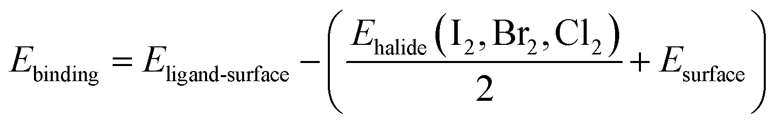
We presented the DFT studies of three kinds of halide ligands (Cl, Br, I) attached to the PbSe surfaces with different crystallographic orientations. Table 1 provides the result of the binding energies of the halide ligands attaching to the surface. The binding energy for one ligand is calculated by following equation:
 | (1) |
| Crystallographic orientation | (001) | (110) | (111) | |||
| Atom bond to ligand | Pb | Se | Pb | Se | Pb | Se |
| Iodine (eV) | −0.310 | −0.133 | −0.354 | 0.027 | −2.302 | −0.501 |
| Bromine (eV) | −0.570 | −0.175 | −0.561 | 0.014 | −2.581 | −0.565 |
| Chlorine (eV) | −0.749 | −0.212 | −0.738 | −0.011 | −2.841 | −0.654 |
Table 1 indicates that halide ligands prefer to bond with Pb atoms rather than with Se atoms due to a lower binding energy. This result agrees well with numerous experimental works that Se atoms are normally capped during the synthesis of PbSe nanostructure and will not introduce extra surface states even without passivation.13,38,39 Therefore, we only study the cases where the halide ligands are connected to Pb atom.
III. Result and discussion
A. Pure surface
Our first step is to simulate the pure surfaces without any ligands and then the results are compared with the ones with ligands. These pure surfaces are relaxed using the slab model mentioned above and we find that the (001) and (110) surfaces are more stable than the (111) surface in terms of surface energies, which is consistent with previous research.24The surface energies, i.e. the energies of the optimized surface in unit area with respect to bulk energy, are used to study the stability of each surfaces, as shown below:40
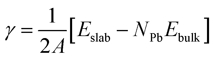 | (2) |
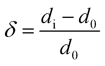
The relaxing of slab layers is defined using the definition mentioned by Ma:25
 | (3) |
| Layers | (001) | (110) | (111)-Pb | (111)-Se |
|---|---|---|---|---|
| a From ref. 24.b From ref. 23.c From ref. 41.d From ref. 26. | ||||
| 1st layer δ1 | −2.9% | −6.3% | −15.3% | −18.9% |
| 2nd layer δ2 | 4.9% | 10.5% | 31.3% | 32.5% |
| 3rd layer δ3 | 0.6% | −3.7% | −14.3% | −14.5% |
| Surface energy γ (meV Å−2) | 25.8 [11.0–25.5]a,b,c,d | 29.7 [19.8–36.7]a,b,c,d | 48.4 [75.3]a | 48.6 [91.9]a |
The instability of the (111) system can be explained by the net dipole field formed between the top (Pb) and the bottom (Se) surfaces of the slab. In contrast, the (001) and (110) surfaces have no net dipole because the Pb and Se atoms are evenly distributed on each surface. The dipole field in the (111) system causes the slab to deform more significantly as can be seen in the relaxing measurement. Both (001) and (110) planes are suffering a similar relaxing level at below 10% respect to bulk PbSe whereas in (111) planes this number is much bigger at around 15% to 30%. In fact, the (110) surface was shown to be rare in the formation of PbSe nano-crystals compared to the other two crystalline orientations.26,42 As PbSe nano-crystals are being synthesized, oleate anions tends to bind more strongly to Pb ions particularly on PbSe (111) planes, which consequently significantly reduces their surface energy. This explains the prevalence of (111) planes over (110) planes, despite their similar high surface energies.23 Compared with other works23,41 on PbSe low-index surface, surface energy of (111) facets appear to be 1.5–2 times of (001) facets which is slight higher.
B. Surfaces with various halide ligands
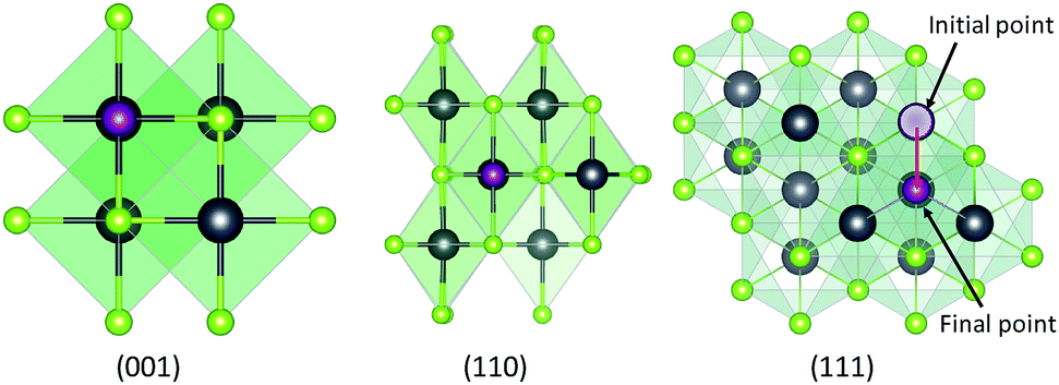 | ||
| Fig. 1 Schematic diagram of PbSe low index surfaces that are 25% covered by halide ligands, left: (001), middle: (110) and right: (111) halide ligands are represented by purple atoms, Pb by grey atoms and Se by green atoms. After optimization ligands attached to exposed Pb atoms in the (111) plane have moved as shown in the plot (red arrow). The hollow sphere represents the initial position of ligand atom. | ||
Fig. 2 shows that in general the distances between ligand atoms and surfaces are proportional to the halide ionic radius. To further analyze the result, the ratio of the distances to the ionic radius of the halide ligand is also computed and we found that the iodine ligand possesses the smallest ratio in (001) and (110) planes and all of them have similar values in (111) planes. Generally, a smaller bond length to ionic radius ratio would lead to better carrier transport between two atoms and this should also be true for nanostructures with halide ligands attached to the surface.
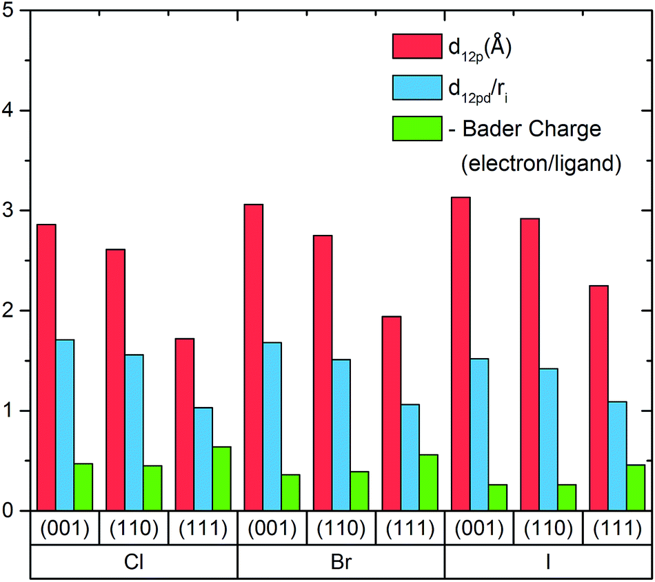 | ||
| Fig. 2 dl2p represents distance from ligand atoms to surface planes, dl2pd/ri represents the ratio between distance from ligand atoms to surface planes and ionic radius of the ligand atom, a smaller ratio means stronger overlapping between ligand atoms and surface planes. Additional Bader charges that transferred from pure surface to ligand atoms has shown where larger number indicates a stronger Bader charge transfer. | ||
Fig. 2 also shows the Bader charges of the ligands for various configurations. It was found that the amount of electron transfer is proportional to the electronegativity of the halide ligands as Cl > Br > I and is inversely proportional to the ionic radius. This implies a more ionic bond in general for small halides, and this increased iconicity of the bond may be responsible for the observed loss of this passivation in humid environments experimentally. It is also observed that ligands bonding to (111) plane possess more Bader charges than those bonding to the other two planes. One reason could be the net dipole in the (111) system generates an electric field perpendicular to the surface. This dipole makes possible the existence of built-in potential perpendicular to the surface that requires extra Bader charge transfer to terminate. A rough indication can be obtained through the change in the lead atom Bader charges on the topmost surface (Tables 1 & 2 in ESI†), which show that in the (111) plane the Bader charge transfer is shared by each of the lead atoms at the top surface whereas for the (001) and (110) planes the negative Bader charges from the ligands are coming from particular lead atoms.
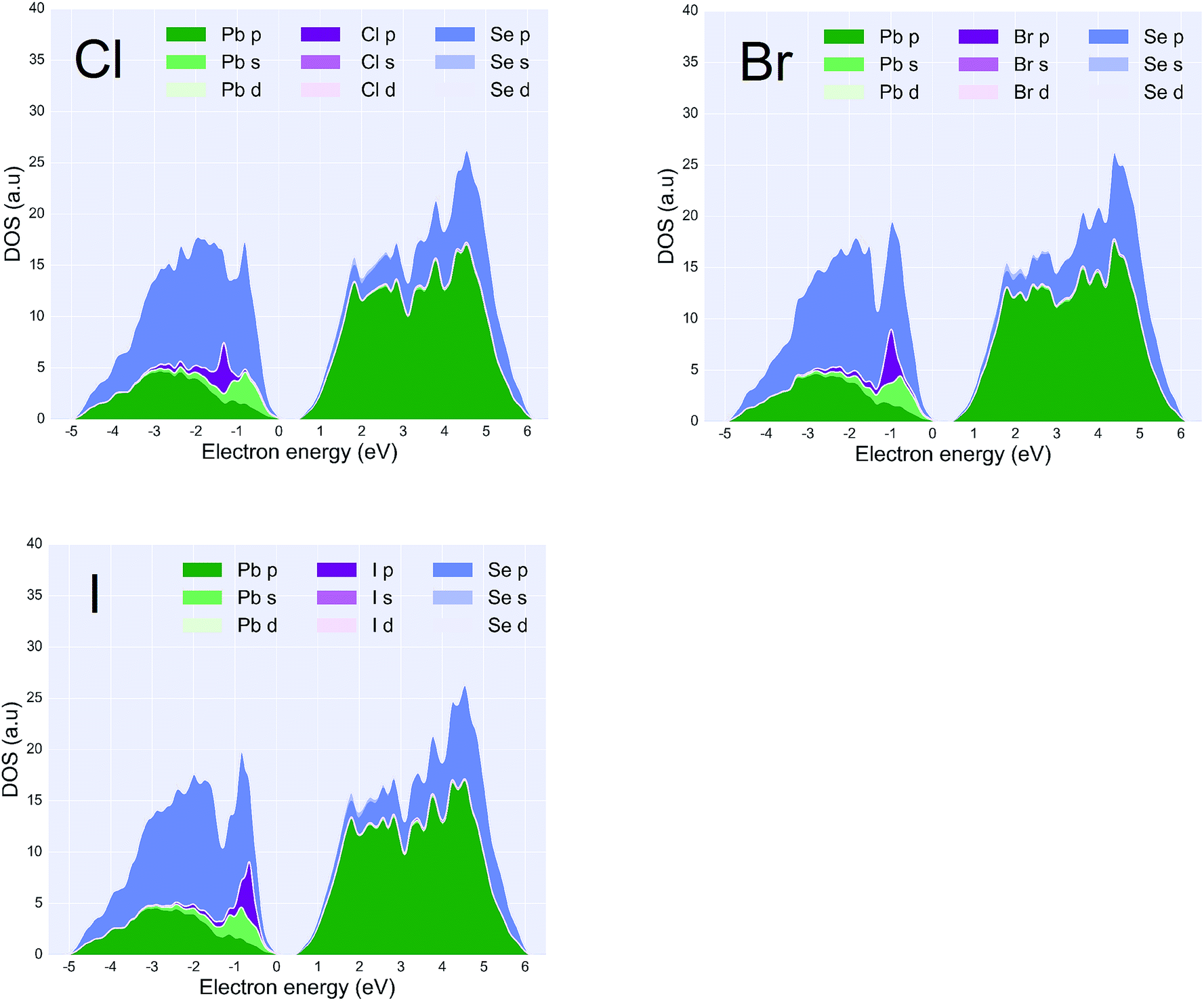 | ||
| Fig. 3 Projected DOS with three types of halide ligands attached to the PbSe (001) surfaces at a coverage density of 25% (upper-left: chlorine ligand, upper-right: bromine ligand, bottom-left: iodine ligand). Size of the surfaces and percentage of ligand coverage. The zero energy corresponds to the highest occupied states at a temperature of zero kelvin. As can be seen, the PDOS of halide p orbital in dark purple is shifting to the edge of the valence bands from Cl to I. | ||
Fig. 3 states at the edge of the conduction bands are dominated by the p-orbital from Pb atoms whereas states at the edge of the valence bands result from the p-orbitals on Se atoms. According to the PDOS, a HOMO–LUMO gap of less than 1 eV is observed in all of the configurations. This suggests that a 25% coverage of halide ligands does not change the bandgap significantly but only adds extra states in the valence bands. It can be seen in the PDOS that the halide p-orbital contribution to the PDOS sits at approximately ∼1 eV lower than the edge of the valence bands. The iodine p-orbital contribution is closer to the valence band edge than the other two halides, and the chlorine p-orbital is the furthest. This suggests that of all the three configurations, the iodine ligand would participate more in the conduction of holes and have a higher probability of hopping conduction. Also, within approximately 1.5 kT from Fermi level, three ligands I, Br, Cl contribute 18.1%, 15.6%, 13.4% of total DOS respectively. Provided that all three ligands perform equally well in terms of passivation, which agrees with experimentation results,45 the iodine ligand should provide a better hopping probability between PbSe nano-crystals. The iodine ligand participates more in the states near the valence band maximum, effectively drawing carriers closer to the surface and increasing the potential for overlap between carriers in that state and those on similar states in neighboring QDs. Such a tendency has been observed in the experiment that PbSe quantum dots with iodine ligand possess a general better current output compared to other halide ligands.19
C. Surfaces with various ligand coverages
There are limited numbers of theoretical studies that show the effect of different ligand coverages on the re-construction of surfaces and the electronic band structure at a detailed level.23,24 The (111)-Pb surface with different amounts of coverage by iodine ligands is of interest due to its large dipole though results for the (100) plane and (110) plane are also presented in ESI Fig. 1.† From Fig. 4, it is apparent that the binding strength for iodine ligands decreases along with the increase of coverage in (111)-Pb plane. A possible reason for this would be the increased coulombic force between the ligand atoms reduced the binding strength between surface and ligands as the ligand density increases. The distances between ionic ligands are much smaller at high densities, leading to potential coulombic repulsions. Experimentally there may be some trade-off between the amount of atomic ligand that migrates into solution and that which remains on the surface as a function of time, since given the opportunity the system will relax to its lowest energy state.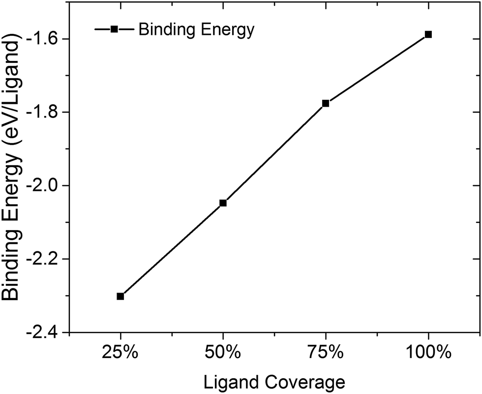 | ||
| Fig. 4 Binding energy of iodine ligands onto PbSe (111)-Pb surface with various coverages. Larger negative number indicates a more stable configuration. | ||
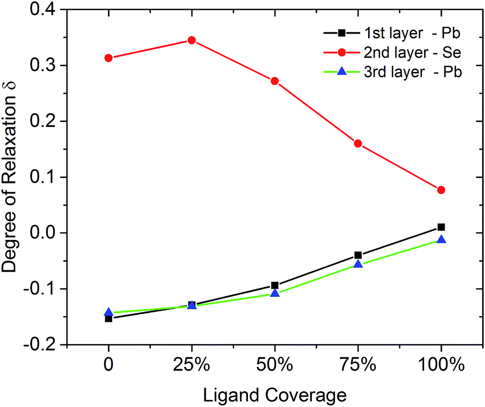 | ||
| Fig. 5 Degree of relaxation δ for PbSe on the (111)-Pb facet showing the topmost 3 layers at different iodine ligand coverages. Relaxation is defined with respect to the lattice constant in the bulk and calculated with the same definition as eqn (3). | ||
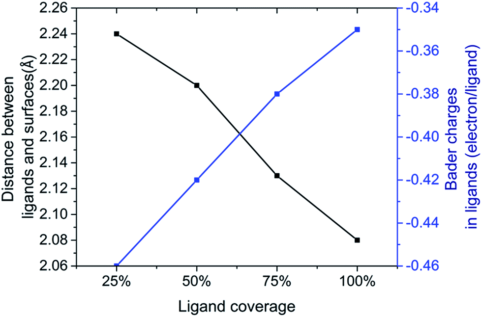 | ||
| Fig. 6 Ligand surface restructuring and Bader charge transfer on (111) PbSe surfaces for iodine ligands along coverage density change. A larger negative number indicates more Bader charge transferred into halide ligand atoms. | ||
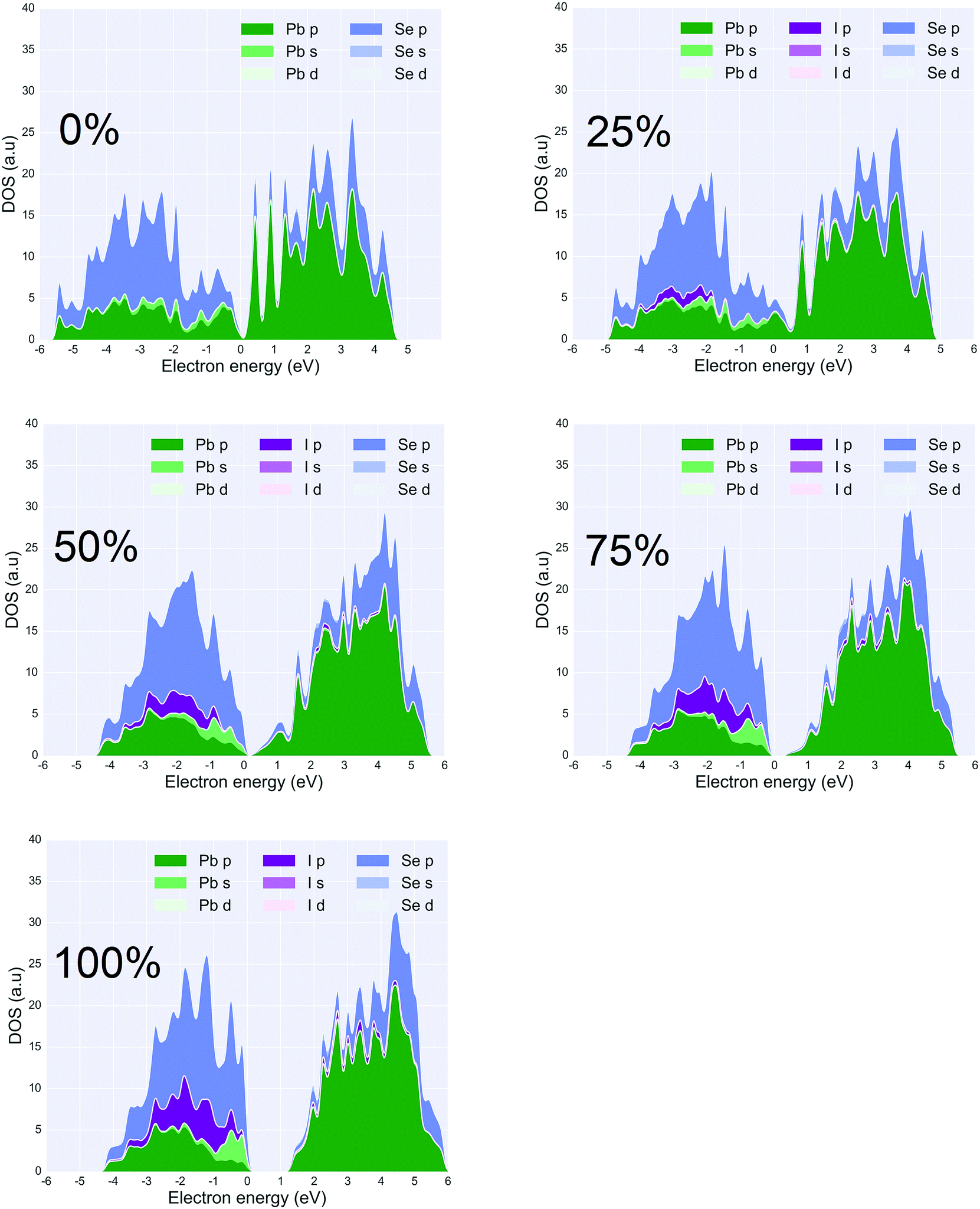 | ||
| Fig. 7 Projected DOS of PbSe (111)-Pb surfaces with five different coverages of iodine ligands (top-left: pristine (111)-Pb surface (0% coverage), top-middle: 25% coverage, top-left: 50% coverage, bottom-right: 75% coverage, bottom-middle: 100% coverage). 100% coverage refers all Pb atoms are passivated by ligands. The bandgap widen would be easily seen along the increase of ligand density. | ||
IV. Conclusion
In this work, we have modelled several low-index of PbSe surfaces with various halide ligands acting as passivation agents with DFT using an LCAO basis.With different inorganic halide ligands (I, Br and Cl), we show that chlorine ligands have the strongest bonding to PbSe surface, followed by bromine and iodine ligands. However, a similar PDOS outcome from all three halide ligands was obtained. Among the three halides, iodine ligands seem to be contributing more conductance in hole's transportation so that PbSe nanocrystals with iodine ligand would be expected to have lower resistance than other two types of ligand in photovoltaic devices.
Modelling of the PbSe surface with various coverage of iodine ligands, mainly focusing on (111) plane showed a strong passivation effect when ligand density has reached some point (more than 50% coverage) as there is a significant band gap widening appears along with coverage more than 50%.
Such changes could also be concluded from the change of relaxation that with increase of passivation, the bond lengths between Pb and Se (interlayer distance) are more close to the number in bulk material.
In this work we have presented a quantitative result with reasonable accuracy as an indication of effect of halide ligand modification on PbSe surface and also discuss the nature of how inorganic surface passivation helps improve the quality of PbSe nanocrystals in emerging technological applications. Further work we wish to present some quantitative results on electrical transport with inorganic ligands present on PbSe surfaces.
Acknowledgements
This program is supported by Australian government through the Australian Renewable Energy Agent. The Australian Government is supporting Australian research in development cost effective photovoltaics.Notes and references
- R. D. Schaller and V. I. Klimov, High Efficiency Carrier Multiplication in PbSe Nanocrystals: Implications for Solar Energy Conversion, Phys. Rev. Lett., 2004, 92, 186601 CrossRef CAS PubMed.
- J. S. Steckel, S. Coe-Sullivan, V. Bulović and M. G. Bawendi, 1.3 Mm to 1.55 Mm Tunable Electroluminescence from PbSe Quantum Dots Embedded within an Organic Device, Adv. Mater., 2003, 15, 1862–1866 CrossRef CAS.
- J. M. Pietryga, R. D. Schaller, D. Werder, M. H. Stewart, V. I. Klimov and J. A. Hollingsworth, Pushing the Band Gap Envelope:
![[thin space (1/6-em)]](https://www.rsc.org/images/entities/char_2009.gif) Mid-Infrared Emitting Colloidal PbSe Quantum Dots, J. Am. Chem. Soc., 2004, 126, 11752–11753 CrossRef CAS PubMed.
Mid-Infrared Emitting Colloidal PbSe Quantum Dots, J. Am. Chem. Soc., 2004, 126, 11752–11753 CrossRef CAS PubMed. - P. R. Brown, D. Kim, R. R. Lunt, N. Zhao, M. G. Bawendi, J. C. Grossman and V. Bulovic, Energy Level Modification in Lead Sulfide Quantum Dot Thin Films through Ligand Exchange, ACS Nano, 2014, 8, 5863–5872 CrossRef CAS PubMed.
- M. C. Beard, J. M. Luther, O. E. Semonin and A. J. Nozik, Third Generation Photovoltaics Based on Multiple Exciton Generation in Quantum Confined Semiconductors, Acc. Chem. Res., 2013, 46, 1252–1260 CrossRef CAS PubMed.
- O. E. Semonin, J. M. Luther and M. C. Beard, Quantum Dots for Next-Generation Photovoltaics, Mater. Today, 2012, 15, 508–515 CrossRef CAS.
- R. J. Ellingson, M. C. Beard, J. C. Johnson, P. Yu, O. I. Micic, A. J. Nozik, A. Shabaev and A. L. Efros, Highly Efficient Multiple Exciton Generation in Colloidal PbSe and PbS Quantum Dots, Nano Lett., 2005, 5, 865–871 CrossRef CAS PubMed.
- A. J. Nozik, Quantum Dot Solar Cells, Phys. E, 2002, 14, 115–120 CrossRef CAS.
- J. A. McGuire, M. Sykora, J. Joo, J. M. Pietryga and V. I. Klimov, Apparent Versus True Carrier Multiplication Yields in Semiconductor Nanocrystals, Nano Lett., 2010, 10, 2049–2057 CrossRef CAS PubMed.
- Z. Zhang, J. Yang, X. Wen, L. Yuan, S. Shrestha, J. A. Stride, G. J. Conibeer, R. J. Patterson and S. Huang, Effect of Halide Treatments on PbSe Quantum Dot Thin Films: Stability, Hot Carrier Lifetime, and Application to Photovoltaics, J. Phys. Chem. C, 2015, 119, 24149–24155 CAS.
- W. Shockley and H. J. Queisser, Detailed Balance Limit of Efficiency of P–N Junction Solar Cells, J. Appl. Phys., 1961, 32, 510 CrossRef CAS.
- V. I. Klimov, Detailed-Balance Power Conversion Limits of Nanocrystal-Quantum-Dot Solar Cells in the Presence of Carrier Multiplication, Appl. Phys. Lett., 2006, 89, 123118 CrossRef.
- I. Moreels, B. Fritzinger, J. C. Martins and Z. Hens, Surface Chemistry of Colloidal PbSe Nanocrystals, J. Am. Chem. Soc., 2008, 130, 15081–15086 CrossRef CAS PubMed.
- D. V. Talapin and C. B. Murray, PbSe Nanocrystal Solids for N- and P-Channel Thin Film Field-Effect Transistors, Science, 2005, 310, 86–89 CrossRef CAS PubMed.
- M. Law, J. M. Luther, Q. Song, B. K. Hughes, C. L. Perkins and A. J. Nozik, Structural, Optical, and Electrical Properties of PbSe Nanocrystal Solids Treated Thermally or with Simple Amines, J. Am. Chem. Soc., 2008, 130, 5974–5985 CrossRef CAS PubMed.
- Y. Liu, M. Gibbs, J. Puthussery, S. Gaik, R. Ihly, H. W. Hillhouse and M. Law, Dependence of Carrier Mobility on Nanocrystal Size and Ligand Length in PbSe Nanocrystal Solids, Nano Lett., 2010, 10, 1960–1969 CrossRef CAS PubMed.
- J. Zhang, J. Gao, E. M. Miller, J. M. Luther and M. C. Beard, Diffusion-Controlled Synthesis of PbS and PbSe Quantum Dots with In situ Halide Passivation for Quantum Dot Solar Cells, ACS Nano, 2014, 8, 614–622 CrossRef CAS PubMed.
- W. K. Bae, J. Joo, L. A. Padilha, J. Won, D. C. Lee, Q. Lin, W.-k. Koh, H. Luo, V. I. Klimov and J. M. Pietryga, Highly Effective Surface Passivation of PbSe Quantum Dots through Reaction with Molecular Chlorine, J. Am. Chem. Soc., 2012, 134, 20160–20168 CrossRef CAS PubMed.
- R. W. Crisp, D. M. Kroupa, A. R. Marshall, E. M. Miller, J. Zhang, M. C. Beard and J. M. Luther, Metal Halide Solid-State Surface Treatment for High Efficiency PbS and PbSe Qd Solar Cells, Sci. Rep., 2015, 5, 9945 CrossRef CAS PubMed.
- A. R. Marshall, M. R. Young, A. J. Nozik, M. C. Beard and J. M. Luther, Exploration of Metal Chloride Uptake for Improved Performance Characteristics of PbSe Quantum Dot Solar Cells, J. Phys. Chem. Lett., 2015, 6, 2892–2899 CrossRef CAS PubMed.
- S. J. Oh, N. E. Berry, J.-H. Choi, E. A. Gaulding, H. Lin, T. Paik, B. T. Diroll, S. Muramoto, C. B. Murray and C. R. Kagan, Designing High-Performance PbS and PbSe Nanocrystal Electronic Devices through Stepwise, Post-Synthesis, Colloidal Atomic Layer Deposition, Nano Lett., 2014, 14, 1559–1566 CrossRef CAS PubMed.
- J. Y. Woo, J. H. Ko, J. H. Song, K. Kim, H. Choi, Y. H. Kim, D. C. Lee and S. Jeong, Ultrastable PbSe Nanocrystal Quantum Dots Via In situ Formation of Atomically Thin Halide Adlayers on PbSe (100), J. Am. Chem. Soc., 2014, 136, 8883–8886 CrossRef CAS PubMed.
- C. R. Bealing, W. J. Baumgardner, J. J. Choi, T. Hanrath and R. G. Hennig, Predicting Nanocrystal Shape through Consideration of Surface–Ligand Interactions, ACS Nano, 2012, 6, 2118–2127 CrossRef CAS PubMed.
- M. Argeri, A. Fraccarollo, F. Grassi, L. Marchese and M. Cossi, Density Functional Theory Modeling of PbSe Nanoclusters: Effect of Surface Passivation on Shape and Composition, J. Phys. Chem. C, 2011, 115, 11382–11389 CAS.
- J.-x. Ma, Y. Jia, Y.-l. Song, E.-j. Liang, L.-k. Wu, F. Wang, X.-c. Wang and X. Hu, The Geometric and Electronic Properties of the PbS, PbSe and PbTe (001) Surfaces, Surf. Sci., 2004, 551, 91–98 CrossRef CAS.
- C. Fang, M. A. van Huis, D. Vanmaekelbergh and H. W. Zandbergen, Energetics of Polar and Nonpolar Facets of PbSe Nanocrystals from Theory and Experiment, ACS Nano, 2010, 4, 211–218 CrossRef CAS PubMed.
- Y. Q. Gai, H. W. Peng and J. B. Li, Electronic Properties of Nonstoichiometric PbSe Quantum Dots from First Principles, J. Phys. Chem. C, 2009, 113, 21506–21511 CAS.
- A. Kutana and S. C. Erwin, PbSe Nanocrystals Remain Intrinsic after Surface Adsorption of Hydrazine, Phys. Rev. B: Condens. Matter Mater. Phys., 2011, 83, 235419 CrossRef.
- A. Franceschetti, Structural and Electronic Properties of PbSe Nanocrystals from First Principles, Phys. Rev. B: Condens. Matter Mater. Phys., 2008, 78, 075418 CrossRef.
- J.-Q. Goh, S. Malola, H. Häkkinen and J. Akola, Role of the Central Gold Atom in Ligand-Protected Biicosahedral Au24 and Au25 Clusters, J. Phys. Chem. C, 2013, 117, 22079–22086 CAS.
- S. R. Bahn and K. W. Jacobsen, An Object-Oriented Scripting Interface to a Legacy Electronic Structure Code, Comput. Sci. Eng., 2002, 4, 56–66 CrossRef CAS.
- J. J. Mortensen, L. B. Hansen and K. W. Jacobsen, Real-Space Grid Implementation of the Projector Augmented Wave Method, Phys. Rev. B: Condens. Matter Mater. Phys., 2005, 71, 035109 CrossRef.
- J. Enkovaara, et al., Electronic Structure Calculations with GPAW: A Real-Space Implementation of the Projector Augmented-Wave Method, J. Phys.: Condens. Matter, 2010, 22, 253202 CrossRef CAS PubMed.
- A. H. Larsen, M. Vanin, J. J. Mortensen, K. S. Thygesen and K. W. Jacobsen, Localized Atomic Basis Set in the Projector Augmented Wave Method, Phys. Rev. B: Condens. Matter Mater. Phys., 2009, 80, 195112 CrossRef.
- J. P. Perdew, K. Burke and M. Ernzerhof, Generalized Gradient Approximation Made Simple, Phys. Rev. Lett., 1996, 77, 3865–3868 CrossRef CAS PubMed.
- W. Tang, E. Sanville and G. Henkelman, A Grid-Based Bader Analysis Algorithm without Lattice Bias, J. Phys.: Condens. Matter, 2009, 21, 084204 CrossRef CAS PubMed.
- E. Sanville, S. D. Kenny, R. Smith and G. Henkelman, Improved Grid-Based Algorithm for Bader Charge Allocation, J. Comput. Chem., 2007, 28, 899–908 CrossRef CAS PubMed.
- Q. Dai, Y. Wang, Y. Zhang, X. Li, R. Li, B. Zou, J. Seo, Y. Wang, M. Liu and W. W. Yu, Stability Study of PbSe Semiconductor Nanocrystals over Concentration, Size, Atmosphere, and Light Exposure, Langmuir, 2009, 25, 12320–12324 CrossRef CAS PubMed.
- U. Kumar, S. N. Sharma, S. Singh, M. Kar, V. N. Singh, B. R. Mehta and R. Kakkar, Size- and Shape-Controlled Synthesis and Properties of Colloidal PbSe Nanocrystals, Mater. Chem. Phys., 2009, 113, 107–114 CrossRef CAS.
- V. L. Deringer and R. Dronskowski, Stabilities and Reconstructions of PbTe Crystal Surfaces from Density-Functional Theory, J. Phys. Chem. C, 2013, 117, 24455–24461 CAS.
- V. L. Deringer and R. Dronskowski, Stabilities and Reconstructions of Clean PbS and PbSe Surfaces: DFT Results and the Role of Dispersion Forces, J. Phys. Chem. C, 2016, 120, 8813–8820 CAS.
- K.-S. Cho, D. V. Talapin, W. Gaschler and C. B. Murray, Designing PbSe Nanowires and Nanorings through Oriented Attachment of Nanoparticles, J. Am. Chem. Soc., 2005, 127, 7140–7147 CrossRef CAS PubMed.
- I. N. Yakovkin and P. A. Dowben, The Problem of the Band Gap in LDA Calculations, Surf. Rev. Lett., 2007, 14, 481–487 CrossRef CAS.
- J. P. Perdew, Density Functional Theory and the Band Gap Problem, Int. J. Quantum Chem., 1985, 28, 497–523 CrossRef.
- Z. Zhang, R. Patterson, S. Shrestha, G. Conibeer and H. Shujuan, in Investigation on Stability of Halide Treated PbSe Quantum Dot Thin Films for Photovoltaic Devices, Photovoltaic Specialist Conference (PVSC), 2015 IEEE 42nd, 14-19 June 2015, 2015, pp. 1–3 Search PubMed.
- R. E. Brandt, V. Stevanović, D. S. Ginley and T. Buonassisi, Identifying Defect-Tolerant Semiconductors with High Minority-Carrier Lifetimes: Beyond Hybrid Lead Halide Perovskites, MRS Commun., 2015, 5, 265–275 CrossRef CAS.
- J. X. Ma, Y. Jia, Y. L. Song, E. J. Liang, L. K. Wu, F. Wang, X. C. Wang and X. Hu, The Geometric and Electronic Properties of the PbS, PbSe and PbTe (001) Surfaces, Surf. Sci., 2004, 551, 91–98 CrossRef CAS.
Footnote |
| † Electronic supplementary information (ESI) available. See DOI: 10.1039/c6ra21668d |
| This journal is © The Royal Society of Chemistry 2016 |