DOI:
10.1039/C6RA21590D
(Paper)
RSC Adv., 2016,
6, 109105-109123
Growth and characterization of semi-organic third order nonlinear optical (NLO) potassium 3,5-dinitrobenzoate (KDNB) single crystals
Received
29th August 2016
, Accepted 10th November 2016
First published on 10th November 2016
Abstract
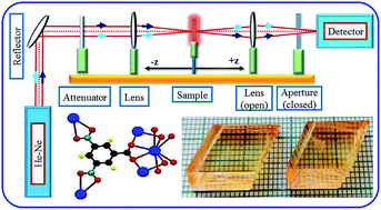
The semi-organic single crystal of potassium 3,5-dinitrobenzoate (KDNB) was successfully grown by slow evaporation solution technique (SEST) at room temperature. The lattice parameters of the grown KDNB crystal were confirmed by single crystal X-ray diffraction. The functional groups of the KDNB crystal were confirmed by Fourier transform infrared (FTIR) spectroscopy analysis. The optical quality of the grown crystal was identified by UV-Vis NIR spectral analysis. The grown crystal has good optical transparency in the range of 410–1100 nm. In the photoluminescence spectrum, sharp broad emission peaks were observed, which indicate violet and blue emission. The photoconductivity study reveals that the grown crystal has a negative photoconductive nature. The thermal behaviour of the crystal has been investigated by thermogravimetric and differential thermal analysis (TG-DTA). Vickers microhardness analysis was carried out to identify the mechanical stability of the grown crystal and the indentation size effect (ISE) was explained satisfactorily by Hays–Kendall's approach and proportional specimen resistance model [PSRM]. A chemical etching study was carried out and the etch pit density (EPD) was calculated. Laser damage threshold (LDT) energy has been measured by using a Nd:YAG laser (1064 nm). The dielectric permittivity and dielectric loss as a function of frequency were measured for the grown crystal. The solid state properties such as plasma energy, Penn gap and Fermi energy were evaluated for the KDNB crystal using the empirical relation. These estimated values were utilized to report the electronic polarizability. This matches well to the value calculated from Clausius–Mossotti relation, Lorentz–Lorentz equation, optical band gap energy and coupled dipole method (CDM). The third-order nonlinear optical properties such as refractive index (n2), absorption co-efficient (β) and susceptibility (χ(3)) were studied using Z-scan technique at 632.8 nm of He–Ne laser.
1. Introduction
In recent years, there has been considerable interest in the study of NLO crystals with good appropriate properties because of their wide applications in the areas of laser technology, optical communications, optical information processing and optical data storage technology,1 color displays, electro-optic switches, frequency conversion etc.2 Most of the organic crystals possess large NLO efficiency but usually have poor mechanical and thermal properties and are susceptible to damage. Inorganic crystals have excellent mechanical and thermal properties, but these possess relatively modest optical nonlinearity because of the lack of extended π-electron delocalization.3,4 Hence, the third phase of semi-organic crystals which combine both the positive aspects of organic and inorganic crystals result in useful nonlinear optical properties. The resultant materials gain importance in the field of nonlinear optics due to their good optical nonlinearity, chemical flexibility, thermal stability and excellent transmittance in the UV-visible region with bulk crystal morphologies.5 Semi-organic single crystals possess higher optical, mechanical and thermal properties. The metal coordination complexes of highly polarizable organic molecules together with the hydrogen bonds, increase the thermal and mechanical stabilities of the crystal. In the prosing KDNB crystal nitro groups are normally bonded to the metal ions through the conjugated π-electron bonding system of donor and acceptor ions, which provides high optical nonlinearity effects like bonding of K+ ion with NO2 group in the crystal.6 The anion and the cation lie on a twofold axis. The K+ cation is surrounded by eight O atoms and the crystal structure is stabilized by π–π interaction. The hydrogen bonds O–H⋯O between carboxyl groups results in the dimerization of 3,5-dinitrobenzoic acid. Extensive hydrogen-bonding interactions generate a two-dimensional wave-like network.7 The nitro-substituted aromatic acid of 3,5-dinitrobenzoic acid has been used to synthesise chiral crystalline adduct materials with physical properties potentially useful in applications such as nonlinear optics.8 The 3,5-dinitrobenzoate anion satisfies the pull–push requirement and it can be approximated to a dipolar NLO chromophores. Also, it has a relatively strong proton donor–acceptor due to the presence of the COOH carboxylic group. There are many reports available about the 3,5-dinitrobenzoic acid bonded to the metals like sodium, lithium,9–11 manganese,12 magnesium,13 potassium,14 cerium,15 calcium,16 strontium,17 zinc and cobalt.18,19 Further, Miminoshvili et al., report the complexes of Co, Ni, Cu and Zn obtained by the reaction of dialkylammonium 3,5-dinitrobenzoates with hydrated metal sulfates in dimethyl sulfoxide.20 The properties of dinitrobenzoic acid with alkali, alkaline, and transition metals have been studied.21 Also, that organic material combines to form crystallization to the amines22–24 and guanidine.25 The interaction between p-phenylenediamine and 3,5-dinitrobenzoic acid has been investigated spectrophotometrically.26 Recently 3,5-dinitrobenzoic acid has been characterized by Chandrasekaran et al.27
In the present investigation, the non-linear optical crystal of potassium 3,5-dinitrobenzoate (KDNB) was grown by slow evaporation solution technique (SEST) and the grown crystals were characterized by single crystal X-ray diffraction (SXRD), Fourier transform infrared (FTIR), UV-Vis NIR, photoluminescence (PL), photoconductivity, thermogravimetric (TG) and differential thermal analysis (DTA), Vickers microhardness, chemical etching, laser damage threshold (LDT), dielectrics, and third order nonlinear optical (Z-scan) studies.
2. Experiment
2.1. Material synthesis, crystal growth and morphology
The analytical reagent (AR) grade of materials potassium hydroxide (KOH) and 3,5-dinitrobenzoic acid (3,5-DNBA) were taken in the stoichiometric ratio 1
:
1 for the synthesis of potassium 3,5-dinitrobenzoate (KDNB) compound. Initially, the calculated amount of KOH and 3,5-DNBA were dissolved in Millipore water of resistivity 18.2 MΩ cm. The strong base of KOH solution was slowly added to insoluble 3,5-DNBA solution. The reactants containing solution were mixed together using mechanical stirring for about 24 hours. After that, it appeared as clear yellow color solution. The prepared solution was allowed uncontrolled evaporation at room temperature. After a few weeks, the obtained yellow color impure crystals were harvested. The purity of the synthesized material was further improved by successive recrystallization process to eliminate impurities. The prepared recrystallized KDNB saturated solution was filtered twice by using Whatman filter paper. The crystallizing dish was used for KDNB crystallization with controlled solvent evaporation. The optically transparent KDNB crystals with the dimensions of 15 × 10 × 5 mm3 have been grown in a period of 30 days. The reaction mechanism of the synthesized KDNB material is depicted in Fig. 1. The photographs of as-grown KDNB crystals are shown in Fig. 2. The morphology of KDNB was indexed by WinXMorph software program. The indexed morphology of KDNB is shown in Fig. 3.
 |
| | Fig. 1 Reaction scheme of KDNB. | |
 |
| | Fig. 2 As grown KDNB single crystal. | |
 |
| | Fig. 3 Morphology of KDNB single crystal. | |
2.2. Solubility
The solubility of KDNB was determined for temperature range 30 °C to 60 °C. The solubility study has been carried out in a constant temperature bath (CTB) with a control accuracy of ±0.01 °C. Initially, the CTB was maintained at 30 °C and continuously stirred with a motorized magnetic stirrer. The solubility was determined by dissolving the recrystallized salts in 100 mL of double distilled water in an air tight container maintained at a constant temperature with continuous stirring. After attaining the saturation, the equilibrium concentration of the solution was analyzed gravimetrically. The same process was repeated to determine the solubility at different temperatures. The variation of solubility with different temperature is shown in Fig. 4.
 |
| | Fig. 4 Solubility curve of KDNB as a function of temperature. | |
3. Characterization studies
The grown KDNB crystal was subjected to the various characterizations to analyze the crystal structure, spectral, optical, thermal and mechanical properties. The Bruker kappa APEXII single crystal X-ray diffractometer with MoKα (λ = 0.71073 Å) was used to measure the unit cell parameters of KDNB crystal. The FTIR spectrum of KDNB crystal was recorded in the range 400–4000 cm−1 using Bruker AXS FTIR spectrometer with ATR accessory mode to analyze the various molecular vibrations of the compound at room temperature. The optical property of the grown crystal was studied using a Perkin-Elmer Lambda-35 UV-Vis NIR spectrophotometer in the region between 200–1100 nm. The photoluminescence measurements of KDNB powder samples were recorded using Jobin Yvon (JY) make fluorolog-FL3-11 spectrofluorometer with xenon arc lamp (450 W) as the excitation source at room temperature. Photoconductivity study was carried out using a Keithley picoammeter (MODEL M6487). The thermal stability was identified by using Perkin-Elmer Diamond TG-DTA instrument. The as grown KDNB crystals were subjected to Vickers microhardness using SHIMADZU HMV-G21 series microhardness tester fitted with the diamond indenter. The surface features of the crystal were identified using COSLAB Model CMM-23 optical microscope trinocular in the reflection mode. A Q-switched Nd:YAG laser (Make: Litron Lasers, UK) of pulse width 10 ns and 10 Hz repetition rate was used for laser damage studies (LDT). The dielectric behavior of KDNB crystal was measured using model PSM 1735 LCR meter in the frequency range 1 Hz to 1 MHz. The Z-scan technique was carried out on the grown KDNB crystal using a continuous wave He–Ne laser (5 mW) of wavelength 632.8 nm with a source diameter 0.5 mm and with peak intensity of 25 MW m−2. The sample was moved along the travelling Z-direction at the focal point and the transmittance was recorded at a finite aperture in the far field as a function of the sample position.
4. Results and discussion
4.1. Single-crystal X-ray diffraction
From the single crystal XRD studies, it was confirmed that the grown crystal belongs to the monoclinic crystal system and the calculated unit cell parameter values are a = 10.17 Å, b = 17.73 Å, c = 7.06 Å, β = 133.03° and volume (V) = 931 Å3, with space group C2/c. The present unit cell parameters of the grown KDNB crystal are in good agreement with the earlier reported values14 and given in Table 1. The molecular structure of KDNB single crystal is shown in Fig. 5.
Table 1 Crystallographic data for KDNB crystal
| Parameters |
Present work |
Reported14 |
| Unit cell dimension |
a = 10.17 Å, b = 17.73 Å, c = 7.06 Å, β = 133.03° |
a = 10.15 Å, b = 17.71 Å, c = 7.06 Å, β = 133.07° |
| Volume |
931 Å3 |
928.1 Å3 |
| Space group |
C2/c |
C2/c |
| System |
Monoclinic |
Monoclinic |
 |
| | Fig. 5 Molecular diagram of KDNB. | |
4.2. FTIR analysis
The molecular vibrations of KDNB crystals were identified by Fourier transform infrared studies and the scanned spectrum is shown in Fig. 6. The each K+ cation interacts with eight O atoms belonging to nitro and carboxylate groups.16 Generally the stretching vibration of C–H band occurs in the region 3100–2800 cm−1. The band at 3096 cm−1 is assigned to the asymmetric stretching and 2860 cm−1 is the symmetric stretching vibrations of
CH group. The very strong asymmetric stretching mode occurs at 1623 cm−1 which indicates the presence of carboxylic salt (COO−) and its symmetric stretching is at 1447 cm−1. Normally aromatic nitro groups absorb strongly at 1530–1500 cm−1 and somewhat more weakly at 1370–1330 cm−1. The peaks at 1525 cm−1 and 1346 cm−1 represent very strong vibration of N
O antisymmetric and symmetric stretching respectively. The peak at 1074 cm−1 is mainly due to C–C bending vibration. The bending vibration of C–N appears at 921 cm−1.28 The very strong C–H out of plane bending vibration is observed at 723 cm−1.8 The C–O wagging vibration is observed at 524 cm−1.
 |
| | Fig. 6 FTIR spectrum of KDNB single crystal. | |
4.3. UV-Vis NIR spectral analysis
The optical properties are closely related to the atomic structure, electronic band gap and electrical properties of the materials. The optical transmittance and absorption spectrum of KDNB single crystal were recorded and the spectrum is shown in Fig. 7. From the UV-Vis NIR spectrum, it is observed that the grown crystal shows good transmission at entire visible and near IR region. The fundamental UV-visible cut off wavelength is found to be at 380 nm. The absorption edge at 450 nm may be assigned to n → π* state. The appearance of the yellow crystal is due to the presence of chromophores such as NO2 and carboxylate group in 3,5-dinitrobenzoate anion.28 Further, the λmax of KDNB crystal is relatively lower than the other DNBA derivatives as given in Table 2. The optical absorption co-efficient (α) dependence on the photon energy (hν) helps to study the band structure and the type of transition of electrons.29 The optical transmittance data have been used to evaluate various optical parameters.
 |
| | Fig. 7 UV-Vis NIR spectrum of KDNB single crystal (thickness of the sample is 1.15 mm). | |
Table 2 Comparison of λmax of KDNB with other DNBA derivatives
| Crystal |
λmax (nm) |
References |
| KDNB |
380 |
Present work |
| 2HADB |
442 |
8 |
| 3,5-DNB (DNBA) |
440 |
27 |
Determination of energy band gap (Eg), extinction co-efficient (K) and refractive index (n0). The absorption co-efficient (α) is determined near the absorption edge at different photon energies. The value of band gap energy (Eg) was estimated from the UV-Vis NIR spectrum.30 The dependence of the optical absorption co-efficient with the photon energy helps to study the band structure and the type of transition of electrons. The quantity α(ν) can be displayed in a number of ways as described by the Tauc's plot relation.31,32where ‘α’ is the absorption co-efficient, ‘hν’ is photon energy, ‘Eg’ is the optical energy band gap, ‘A’ is a constant and ‘m’ is the characteristics of transition.The electron transition between the valence band and conduction band can either be direct or indirect and also both possess forbidden transition.33 The transition number (m) is 1/2 for direct allowed transition, 2 for indirect allowed transition, 3/2 for direct forbidden transition and 3 for indirect forbidden transition.34 In this case, we have to determine the value of ‘m’ and can assume the optical transition nature of KDNB crystal. Taking logarithm on both sides and differentiating the eqn (1) with respect to ‘hν’ we get the following form:35,36
| |
ln(αhν) = ln(A) + m ln(hν − Eg)
| (2) |
| |
 | (3) |
The value of ‘Eg’ can be calculated from a graph plotted between [ln(αhν)]/hν and hν which is shown in Fig. 8(a). The discontinuity in line gives the information about both single37 and multiple38 optical transitions, these are indicated at a particular maximum energy value where a particular transition might have taken place corresponding to a specific value of ‘m’. In this case there is a single stage of optical transition with discontinuity at a particular maximum energy value of knee point (Eg = 3.285 eV). Plotting the graph between [ln(αhν)] and [ln(hν − Eg)] the value of ‘m’ is obtained. The value of ‘m’ was found to be 0.41 ≈ 0.5 ≈ 1/2 by extrapolating linear fit as shown in Fig. 8(b). This confirms that the optical transition of KDNB crystal is allowed direct band gap nature. From the Tauc's plot relation has been rearranged as given below for direct allowed transition:
| |
 | (4) |
 |
| | Fig. 8 (a) Plot of [ln(αhν)]/hν vs. hν and (b) plot of [ln(αhν)] vs. [ln(hν − Eg)]. | |
A graph is plotted between photon energy (hν) and (αhν)2. By extrapolating the linear portion of the curve to zero absorption as shown in Fig. 9(a)
| |
 | (5) |
where ‘
T’ is the transmittance (%), ‘
t’ is the thickness of the sample (1.15 mm) and the co-efficient 2.3026 arises from the conversion factor ln(10) or 1/[log
10(
e)]. The calculated direct band gap energy of KDNB single crystal was 3.20 eV. Theoretical optical band gap energy of KDNB crystal was calculated using the following formula:
| |
 | (6) |
where ‘
λ’ is the lower cut-off wavelength (380 nm). The band gap of the grown KDNB crystal is found to be 3.26 eV, which is in good agreement with the value obtained from
Fig. 8(a) and
9(a). The extinction co-efficient (
K) explains the amount of absorption when electromagnetic wave propagates through a medium and it can be found out using the following relation:
| |
 | (7) |
where ‘
α’ is the absorption co-efficient and ‘
λ’ is the wavelength of light.
Fig. 9(b) shows the variation of extinction co-efficient (
K) with wavelength. The reflectance (
R) and refractive index (
n0) in terms of the absorption co-efficient can be derived from the following relation.
39,40| |
 | (8) |
 |
| | Fig. 9 (a) Optical band gap spectrum, wavelength dependence of (b) extinction co-efficient (K), (c) reflectance (R) and (d) refractive indices (n0). | |
It is observed that reflectance (R) increases with an increase in the photon energy and it is shown in Fig. 9(c). Besides providing information on the transmission (T) and reflectance (R) spectra can be used to calculate the refractive indices (n0) of a KDNB crystal from following equation.
| |
 | (9) |
The linear refractive index (n0) of KDNB crystal was determined in terms of reflectance (R) using the relation (9). The linear refractive index (n0) of the grown crystal is found to be 2.07 at the wavelength of 632.8 nm. Fig. 9(d) shows the variation of refractive index (n0) as a function of wavelength and it can be used to calculate the third order nonlinear optical susceptibility (χ(3)) of KDNB crystal. The optical studies revealed that KDNB crystal possesses good optical behaviour for practical device applications.
4.4. Photoluminescence studies
Photoluminescence is the spontaneous emission of light radiation by the absorption of photons. Although the excitation energy is typically in the form of photons, it could also be generated by an electric field or by ionizing radiation. In the solid state, ligand–ligand interactions are important for applications that involve charge transport and to obtain tunable emission colors.41 The KDNB crystal was excited at 350 nm. The emission spectrum was recorded in the range between 370–600 nm and it is shown in Fig. 10. Excitation and emission wavelength were obtained by changing the excitation wavelength under a fixed emission wavelength and vice versa. Generally, photoluminescence phenomenon is expected in aromatic molecules which contain multiple conjugated bonds leading to a high degree of resonance stability. KDNB crystal consists of phenoxy ion (benzene derivative) having delocalized π-electrons in C
C bonds. The C
C bonds can have different energy spacing between ground and excited states.42 Hence, it emits different mode of radiations. One mode is the broad emission peaks observed at 397 and 418 nm which may be due to the vibrations in crystal lattice by changing thermal energy on it.43 This luminescence emission is in violet region. Another one is a sharp peak emission at 450 nm, which may be due to NH2 group. From 450 nm onwards the intensity is gradually decreased due to the presence of hydrogen bond in the crystal lattice.44 It indicates that a KDNB crystal has a blue luminescence emission.27 The results show that KDNB crystal may have suitable applications in violet and blue-emitting diodes.
 |
| | Fig. 10 Photoluminescence of KDNB single crystal. | |
4.5. Photoconductivity
Photoconductivity measurement was carried out on a cut and well-polished KDNB single crystal by fixing it onto a microscope slide. The electrical contacts were made with the sample by silver paste and it was connected by copper wire. The two electrodes were connected to the DC power supply and their potential is varying from 1–20 V with step voltage of 1 V s−1. The schematic diagram of photoconductivity is shown in Fig. 11. The light from halogen lamp of 50 W was focused on the crystal. Initially the dark current was recorded by keeping the crystal unexposed to any radiation. The photocurrent was measured by applying the same voltage under light illumination also. Fig. 12 shows that the dark current is always higher than the photocurrent, thus confirming the negative photoconductivity nature. The phenomenon of negative photoconductivity is explained by Stockmann model.45 This is due to the reduction in the number of charge carriers or their lifetime in the presence of radiation.46 The decrease of charge carrier (current) or lifetime with illumination could be due to the trapping process and the relation gives the life times of charge carrier.| |
 | (10) |
where ‘v’ is the velocity of the recombination carriers, ‘s’ is the capture cross-section of the recombination centers and ‘N’ is the carrier concentration. As intense light continuously falls on the KDNB crystal, the recombination of electrons and holes take place resulting in decrease in the number of mobile charge carriers, giving rise to negative photoconductivity. Negative photoconductivity materials can be used for UV and IR detector applications.45
 |
| | Fig. 11 Circuit diagram for field dependent conductivity. | |
 |
| | Fig. 12 Photoconductivity of KDNB crystal. | |
4.6. Thermal studies
The thermal stability of the grown KDNB single crystal was studied using TG-DTA. 2 mg of KDNB powder sample was taken in alumina crucible. Nitrogen gas was allowed inside the furnace to maintain a constant inert atmosphere for the entire experiment. The KDNB powder sample was heated in the range of 30 °C to 450 °C with the heating rate of 5 °C min−1. It provides reliable information about the mass and energy changes of the sample with respect to the increasing temperature. The TG and DTA graph is shown in Fig. 13. The KDNB compound exhibits a single stage decomposition point starting around 340 °C with the mass loss of almost 95% of the material. It is due to the liberation of volatile reaction products such as NO2, NO, CO2 and CH.28,47 The remaining 5% of the sample may be carbon. In the present case, there is no weight loss observed between 30 °C to 330 °C. It shows that the crystal was thermally stable upto 330 °C. The DTA curve shows prominent single exothermic peak which illustrates the decomposition of the KDNB compound between 335 °C to 360 °C. From the DTA curve, there is phase transition (solid to gas) and melting was not observed below the exothermic peak at 360 °C. The sharp exothermic peak is attributed to the utilization of thermal energy to overcome the bonding between the potassium cation and the 3,5-dinitrobenzoate anion during the initial stage of decomposition. The thermal stability of KDNB crystal is much higher than the other compounds8,26,48–50 as shown in Table 3.
 |
| | Fig. 13 TG-DTA analysis of KDNB single crystal. | |
Table 3 Comparison of thermal stability DNBA derivatives
| Compound |
Thermal stability (°C) |
References |
| KDNB |
330 |
Present work |
| Li (DNB) and PHEN complex |
208 |
49 |
| DNBA |
205 |
48 |
| [(PPD)(DNB)] complex |
174.93 |
26 |
| 2HADB |
158 |
8 |
| [(3,5-Dinitrobenzoic acid), (4,4′-bipyridyl)] |
158 |
50 |
| [(3,5-Dinitrobenzoic acid), (2,2′-bipyridyl)] |
148 |
50 |
4.7. Microhardness studies
The mechanical strength of the single crystal is very important and it plays a key role in the practical device fabrication. Transparent KDNB single crystals free from cracks, with flat and smooth faces are chosen for static indentation Vickers microhardness test. The crystal has been mounted on the base of the microscope and several loads like 2 g, 5 g, 10 g, 25 g, 50 g and 100 g were given to the top surface of the KDNB crystal plane (010) at different places using 115° triangular pyramid indenter. The static indentations were made with a constant indentation time of 5 s for all the loads. For each load the diagonal length (d) was observed and the average of these values was considered. The Vickers hardness number (Hv) is calculated using the following relation:51| |
 | (11) |
where ‘P’ is the applied load (kg) and ‘d’ is the diagonal length (mm). A plot obtained between the hardness number (Hv) and the applied load (P) is depicted in Fig. 14(a). It shows that the hardness number increases with the increase of applied load upto 50 g and related to indentation size effect (ISE), which indicates that the crystal exhibits reverse indentation size effect (RISE).52 With further increment of load more number of micro-cracks appeared on the crystal surface. This feature is better revealed from the plots of ‘Hv’ against indentation diagonal ‘d’ as seen in Fig. 14(b). In order to obtain experimental data on the load dependence of radial cracks developed at the corner of indentations. The indentation impressions obtained for different loads on KDNB crystal are shown in Fig. 15. For each load, the average length (l) of these cracks was measured manually using an optical microscope from the center of indentation to the crack tip on both diagonals of four cracks. The length (l) of radial cracks is related to function of applied load (P) for indentation by the empirical relation:53where ‘C1’ and ‘m1’ are constants. The value of ‘m1’ is obtained from plots between ‘log
l’ and ‘log
P’ and is shown in Fig. 16(a). Further empirical relation51 between radial crack length (l) and indentation diagonal (d) is given bywhere ‘C2’ and ‘m2’ are constants. The plots of ‘log
l’ against ‘log
d’ are presented in Fig. 16(b). The value of ‘m2’ has been obtained from this graph. Therefore, the value of work hardening co-efficient (n) can be calculated using following equation from obtained values of ‘m1’ and ‘m2’, and the value of ‘n’ was found to be 2.56.| |
 | (14) |
 |
| | Fig. 14 (a) Variation of Hv vs. load P and (b) variation of Hv vs. diagonal (d). | |
 |
| | Fig. 15 Indentation of KDNB crystal. | |
 |
| | Fig. 16 (a) Crack length (log l) vs. load (log P), (b) crack length (log l) vs. diagonal (log d), (c) load P vs. l3/2 and (d) plot of load (log P) vs. diagonal (log d). | |
The fracture mechanics in the indentation process has provided an equilibrium relation54 for a well-developed crack extending under loading conditions. The resistance to fracture indicates the toughness of a material and fracture toughness (Kc) gives how much fracture stress is applied under uniform loading. The fracture toughness (Kc) is given by the relation (15). It is based on the assumption that nucleation of the cracks is due to the development of elastic stress during the course of indentation:55,56
| |
 | (15) |
where ‘
P’ is the applied load in ‘g’, ‘
l’ the crack length measured from center of indentation to crack tip, ‘
d’ the diagonal length of the impression in ‘μm’ and ‘
β0’ is taken as 7 for the Vickers indenter. The relation between ‘
P’ and ‘
l3/2’ gives the average value of the fracture toughness which is shown in
Fig. 16(c)
The brittleness is an important property, it tells about the fracture induced in a material without any appreciable deformation. The value of brittleness index ‘Bi’ is computed using the relation:57
| |
 | (16) |
The relation between the applied load (P) and indentation size (d) is given by Meyer's law.58
where ‘
A’ is arbitrary constant for a given material and ‘
n’ the work hardening co-efficient of the KDNB single crystal. For the normal ISE behaviour exponent
n < 2. When
n > 2, there is the reverse ISE behaviour. When
n = 2, the hardness is independent of applied load and is given by Kick's law. The value of ‘
n’ can be calculated from the Meyer's graph of ‘log
P’
versus ‘log
d’ and fitting data by least squares gives straight line graphs shown in
Fig. 16(d). The value of ‘
n’ was found to be 2.6, which is in good agreement with the value obtained from
eqn (14).
It was confirmed that the grown KDNB crystal belongs to the class of soft material category. In the present case, the yield strength (σy) of the material can be calculated from the hardness value (Hv) as Meyer's index was found to be 2.6 (2 < n < 3) by the following relation:
| |
 | (18) |
A plot of load (P) dependent yield strength (σy) is shown in Fig. 17(a). Also, the elastic stiffness constant (C11) was calculated using Wooster's empirical relation.59 It gives a broad idea about the interatomic bonding strength of the materials.
| |
 | (19) |
 |
| | Fig. 17 (a) Plot of yield strength (σy) vs. load P, (b) variation of stiffness constant (C11) with load P, (c) plot of load P vs. d2 and (d) plot of P/d vs. d. | |
Fig. 17(b) shows the plot between load (P) and stiffness constant (C11) for the KDNB crystal. The calculated Vickers hardness values (Hv), yield strength (σy), stiffness constant (C11), fracture toughness (Kc) and brittleness (Bi) values of KDNB crystal for different loads are given in Table 4.
Table 4 Microhardness (Hv), yield strength (σy), stiffness constant (C11), fracture toughness (Kc) and brittleness values (Bi) of KDNB crystal
| Load P (g) |
Hv (kg mm−2) |
σy (GN m−2) |
C11 × 1014 (Pa) |
Kc (g μm−3/2) |
Bi (μm−1/2) |
| 2 |
9.27 |
7.42 |
0.84 |
0.0090 |
1.0262 |
| 5 |
11.82 |
9.46 |
1.29 |
0.0136 |
0.8673 |
| 10 |
17.02 |
13.63 |
2.45 |
0.0213 |
0.7989 |
| 25 |
20.12 |
16.11 |
3.28 |
0.0303 |
0.6624 |
| 50 |
21.28 |
17.04 |
3.62 |
0.0376 |
0.5649 |
| 100 |
19.30 |
15.46 |
3.05 |
0.0416 |
0.4636 |
According to the Hays–Kendall's approach,60 nonlinear behavior of hardness material can be analytically explained by using the following expression:
where ‘
W’ is the minimum load to initiate plastic (permanent) deformation in gram (g), ‘
A1’ is the load-independent constant. The values of ‘
W’ and ‘
A1’ have been estimated from the plots drawn between the experimental data as ‘
P’
versus ‘
d2’ shown in
Fig. 17(c). The resultant value of ‘
W’ becomes negative, hence the grown crystal of KDNB is exhibiting behaviour of RISE.
61 The corrected indentation-size independent hardness (
H0) has been determined using the following relation:
The values of ‘W’ and ‘H0’ are −4.198 g and 0.0194 g μm−2 respectively for KDNB crystal. The resultant values of W, A1 and H0 are given in Table 5.
Table 5 Results of constant W, A1 and H0 for Hays–Kendall's approach
| Hays–Kendall's approach |
Results |
| Resistance pressure (W) (g) |
−4.198 |
| Load independent constant (A1) (g μm−2) |
0.0105 |
| Corrected hardness (H0) (g μm−2) |
0.0194 |
Proportional specimen resistance model [PSRM] was proposed by several workers62–65 and its behaviour may be described by the relation:
where the parameter ‘
a’ characterizes the load dependence of hardness and ‘
b’ is a load independent constant. The term ‘
ad’ has been attributed to the specimen surface energy,
65,66 the deformed surface layer,
67 the indenter edges acting as plastic hinges
62 and the proportional specimen resistance.
64 The constant ‘
b’ can be obtained from the plots of ‘
P/
d’ against ‘
d’ which is shown in
Fig. 17(d). From the
eqn (22) we can obtain value of ‘
a’ as
| |
 | (23) |
It should be noted that a > 0 results in the appearance of normal ISE in which ‘Hv’ decreases with an increase in indentation diagonal (d). However, when a < 0 for reverse ISE behaviour, in which ‘Hv’ decreases with an increase in indentation diagonal (d). According to Li and Bradt,64 the value of ‘a’ is positive when elastic surface stresses are compressive and it becomes negative when surface stresses are tensile, which lead to a relaxation of these surface stresses introduced by indentation. The corrected indentation-size independent hardness value can be calculated by the relation:
The value of ‘H′0’ was found to be 0.0257, calculated other parameters are ‘a’, ‘b’, ‘ad’ and H′0 and are given in Table 6, which are in good agreement with the values obtained from Hays–Kendall's approach.
Table 6 Results of constant ‘a’, ‘ad’, ‘b’ and H′0 for PSRM
| Proportional specimen resistance model [PSRM] and results |
| Load dependent hardness (a) (g μm−1) |
| 2 g |
5 g |
10 g |
25 g |
50 g |
100 g |
| −0.178 |
−0.210 |
−0.155 |
−0.146 |
−0.159 |
−0.341 |
| Resistance pressure (ad) (g) |
−3.56 |
| Load independent constant (b) (g μm−2) |
0.0139 |
| Corrected hardness (H′0) (g μm−2) |
0.0257 |
4.8. Chemical etching analysis
The chemical etching analysis was carried out for as grown KDNB single crystal to determine the distribution of dislocations and surface features. Good quality and transparent KDNB crystal was used and it is soaked with Millipore water as an etchant. The surface layer features of the grown KDNB crystal were identified by an optical microscope. Well defined elongated rectangular shaped etch pits have been obtained with the various etching time. Fig. 18(a) shows the as grown surface of KDNB crystal. Fig. 18(b–d) shows the photographs of etch pit patterns obtained for 5 s, 10 s and 15 s respectively. Randomly distributed and strictly oriented etch pits were seen. With the increment of etching time, the etch pits size were enlarged and finally the etch pits are overlapped. The density of etch pits was calculated using following equation.| | |
Etch pit density (EPD) = (number of etch pits)/(area)
| (25) |
 |
| | Fig. 18 Chemical etch pits of KDNB single crystal on (010) plane, (a) as grown crystal, (b) 5 s (c) 10 s and (d) 15 s etched surface. | |
The calculated etch pit density (EPD) was 15 × 103 cm−2. The obtained etch pit should have resulted from the internal structural symmetry of the crystal.68,69
4.9. Laser-induced damage threshold studies
The operation of NLO devices depends not only on the linear and nonlinear optical (NLO) properties but also on the ability to withstand high-power laser intensities source.70 Hence, high optical surface damage tolerance is extremely important in the performance of nonlinear optical (NLO) and optoelectronic device applications.71,72 In the present study, the laser damage threshold value of KDNB crystal was measured using a Q-switched pulsed Nd:YAG (wavelength = 1064 nm) laser operating in transverse mode (TM00) and pulse width of 10 ns in the frequency rate of 10 Hz. Laser beam diameter of 1 mm was used to irradiate on the well-polished KDNB crystal surface. The output of the incident laser beam was controlled with a variable attenuator and that crystal was placed at the focus of the converging lens of focal length 35 cm. During laser irradiation, damage of the surface can be determined by the visual formation of damage and the input laser energy density was recorded by a power meter (model no. EPM 2000). The surface damage of KDNB crystal as microscopic image is shown in Fig. 19. The surface damage threshold of the grown KDNB crystal was calculated using the expression:73| |
 | (26) |
where ‘E’ is the input energy density (mJ), ‘τ’ is the pulse width (ns) and ‘r’ is the radius of the circular spot (cm). The calculated value of laser damage threshold value of KDNB was found to be 2.05 GW cm−2, which is higher than KDP, urea74 and other standard NLO materials like KNbO3, LiNbO3, LFMH and LHDPDH75–77 (Table 7). Hence, the grown crystal has good optical damage tolerance. Thus, the KDNB crystal is useful for high power laser applications.
 |
| | Fig. 19 Microscopic images of the LDT pattern. | |
Table 7 Laser damage threshold value of KDNB with reported NLO crystals
| Crystal |
Laser damage threshold (GW cm−2) |
References |
| KDNB |
2.05 |
(Present work) |
| LHDPDH |
1.884 |
77 |
| LFMH |
1.518 |
76 |
| Urea |
1.5 |
74 |
| KNbO3 |
1 |
75 |
| LiNbO3 |
0.3 |
75 |
| KDP |
0.2 |
74 |
4.10. Dielectric studies
The cut and polished single crystals of KDNB were used for dielectric studies. The silver coating was applied on the opposite faces. The coated sample was placed in a hot air own at 100 °C for silver paste to tightly stick to both sides of the sample. This is beneficial for reducing air gaps between them to avoid external polarization by the air molecules. The surface of the sample has a good ohmic contact to the both electrodes without any short circuit condition. Then it is placed between two copper electrodes to form the parallel capacitor. The dielectric permittivity and dielectric loss of the grown KDNB crystal was carried out as a function of frequency from 1 Hz to 1 MHz and is shown in Fig. 20(a) and (b) respectively. From the plot, it is observed that the dielectric permittivity is relatively higher in the lower frequency region and decreases further with an increase in the frequency. The high value of dielectric permittivity is attributed to high ionic conductivity.78 Normally dielectric permittivity of the material depends on the contributions of electronic, ionic, orientation and space charge polarizations. These polarizations are active at lower frequencies. At higher frequency the dielectric permittivity becomes less due to significant loss of the polarizations.79 The dielectric permittivity is calculated by the relation:| |
 | (27) |
where ‘A’ is the area of cross-section, ‘d’ is the thickness of the sample and ‘ε0’ is the permittivity of free space (8.854 × 10⁻¹² F m−1). One of the important factors in the dielectric is power dissipation. It is directly proportional to the dielectric loss ‘tan
δ’ and it also represents the defect and imperfection of crystalline sample. The ac conductivity (σac) has been calculated using the expression:77| |
σac = 2πfε′ε0 tan δ
| (28) |
where ‘ε0’ is the permittivity of free space, ‘ε′’ is the relative dielectric permittivity of KDNB crystal and ‘f’ is the applied frequency (Hz). The variation of ac conductivity with applied frequency is shown in Fig. 20(c).
 |
| | Fig. 20 (a) Dielectric permittivity, (b) dielectric loss and (c) ac conductivity of KDNB crystal at the temperature of 35 °C. | |
4.11. Dielectric solid state parameters
Solid state parameters are important in electro-optic polarizability of the material and it is essential for the desired efficiency of nonlinear effect. Theoretical calculation shows that the high frequency dielectric constant explicitly depends on the valence electron plasma energy, Penn gap, Fermi energy and electronic polarizability. The density of KDNB is calculated by using the following equation.| |
 | (29) |
where the molecular weight of the grown KDNB crystal is M = 250.21 g mol−1, molecular unit cell Z = 4, NA is Avogadro's number (6.023 × 10²³) and the volume of unit cell V = 928.1 Å3. The calculated density of KDNB crystal is 1.79 g cm−3. The valence electron plasma energy (ħωp) is given by80| |
 | (30) |
where the total number of valence electrons of KDNB crystal is Z′ = [(1 × Z′K) + (7 × Z′C) + (3 × Z′H) + (2 × Z′N) + (6 × Z′O)] = 78. It can be calculated by substituting for each atom of K, C, H, N and O as corresponding valence electrons are 1, 4, 1, 5 and 6 respectively. The dielectric permittivity (ε′) at 1 MHz was calculated to be 164. According to the Penn model,81 the average Penn gap (EP) and Fermi energy (EF)82 for KDNB are calculated using the following two relations:| |
 | (31) |
| |
 | (32) |
Then, we can calculate the electronic polarizability (α) of the KDNB crystal using the following relation:83
| |
 | (33) |
where ‘
S0’ is a constant for a particular material which is given by
| |
 | (34) |
The value of electronic polarizability (α) is also confirmed by using the Clausius–Mossotti relation,84 which is in good agreement with the value obtained from the eqn (33).
| |
 | (35) |
According to Maxwell relation, for visible light (high-frequency electric field), the dielectric permittivity is equal to the square of the refractive index (ε′ = n02). The relationship between the electronic polarizability (α) and refractive index (n0) in such fields is described by the Lorentz–Lorenz equation85 given by
| |
 | (36) |
The value of electronic polarizability (α) can also be obtained using optical band gap, which is given by
| |
 | (37) |
where ‘
Eg’ is the optical band gap (eV) of the KDNB crystal.
Electronic polarizability based on coupled dipole method (CDM) was introduced by Renne and Nijboer in the 1960.86,87 In the CDM, each atom in a cluster is treated as a Lorentz atom (Drude oscillator), in which the electron is bound to the nucleus by a harmonic force. The atoms have no permanent electric dipole moment, but their dipole moments are induced by the local electric field, so that, if the electron is at a nonzero distance from the nucleus, the atom is effectively an induced electric dipole. Therefore the electronic polarizability (α) of KDNB crystal has been calculated using relation:88
| |
 | (38) |
where
Z′ is the total number of valence electrons, the charge of electron (
e) is 1.602 × 10
−19 C and mass (
me) is 9.1 × 10
−28 g and ‘
ω0’ is the natural frequency (2π
f0),
f0 is 1 MHz. All these calculated parameters for the KDNB crystal are higher than the KDP
37 listed in
Table 8. Dielectric susceptibility (
χ) is obtained using the relation:
| |
 | (39) |
| |
 | (40) |
Table 8 Electrical properties for the grown KDNB crystal
| Parameters |
Values of KDNB crystal |
Values of KDP crystal39 |
| Plasma energy ℏωp (eV) |
21.516 |
17.33 |
| Penn gap energy EP (eV) |
1.685 |
2.39 |
| Fermi energy EF (eV) |
17.642 |
12.02 |
| Electronic polarizability (α) using Penn analysis (cm3) |
5.43 × 10⁻²³ |
2.14 × 10⁻²³ |
| Electronic polarizability (α) using Clausius–Mossotti equation (cm3) |
5.44 × 10⁻²³ |
2.18 × 10⁻²³ |
| Electronic polarizability (α) using Lorentz–Lorentz relation (cm3) |
2.14 × 10⁻²³ |
— |
| Electronic polarizability (α) using optical band gap (cm3) |
3.09 × 10⁻²³ |
— |
| Electronic polarizability (α) using CDM (cm3) |
5.57 × 10⁻²³ |
— |
The KDNB crystal has higher value of electronic polarizability (α) and these values are in good agreement with each other.
4.12. Z-Scan studies
The third-order NLO properties of KDNB crystal were investigated using Z-scan technique to determine the third order nonlinear refractive index (n2) and nonlinear absorption co-efficient (β) simultaneously.83,89 In this experiment, the third-order NLO properties of the KDNB crystal were investigated by using He–Ne laser (5 mW) of wavelength at 632.8 nm as a source and the beam diameter is 0.5 mm. Laser was focused with Gaussian filter to convert input laser beam into Gaussian form. The polarized Gaussian beam of mode TEM00 was focused by a convex lens (focal length is 30 mm) to produce the beam waist ω0 = 12.05 μm. The thickness of sample (L) is 0.52 mm. The Rayleigh length (ZR) was calculated as 0.7207 mm using the formula:| |
 | (41) |
The factor of Rayleigh length (ZR > L) was satisfied for this condition. The sample was fixed on a holder (90°) and it moved along the negative (−Z) to positive (+Z) axis, which is the direction of propagation of the laser beam. The translation of sample holder can be controlled by computer for precision of each movement. The corresponding transmitted intensity through the sample was collected by a photodetector and it was measured by the digital power meter. In closed aperture, the received intensity depends on the aperture radius (2 mm) and it is consistent for entire process. For an open aperture method, intensity was collected directly by placing lens in front of the detector to find out nonlinear absorption co-efficient (β) and the aperture was placed between lens and the front of the detector in order to resolve the nonlinear refraction (n2) of KDNB crystal. Fig. 21(a) and (b) depict the closed and open aperture Z-scan curves of KDNB crystal. The intensity of a laser beam directly depends on refractive index of the materials and its absorption nature. The sample causes an additional focusing or defocusing, depending on the nonlinear refraction values.90 The maximum transmission at the focus (Z = 0) is indicative of the saturation of absorption at high intensity.91 From the open aperture Z-scan spectrum the non-linear absorption co-efficient (β) can be calculated. However, the closed aperture Z-scan curve with pre-focal peak and post-focal valley indicates a self-defocusing process and a negative sign for nonlinear refraction.92 The schematic setup of the Z-scan technique is depicted in Fig. 22. Also it shows the general behaviour of nonlinear refractive index (positive or negative) and absorption (saturated or multi-photon) for close and open aperture respectively.
 |
| | Fig. 21 (a) Closed aperture mode and (b) open aperture mode Z-scan plot of KDNB crystal. | |
 |
| | Fig. 22 Experimental setup of Z-scan technique. | |
In order to find out nonlinear refractive index of KDNB crystal, the difference between the transmittance peak and valley transmission (ΔTp–v) can be written in terms of the on – axis phase shift at the focus.
| |
 | (42) |
where ‘Δ
φ’ is the axis phase shift at the focus, ‘
S’ is the linear transmittance aperture and it was calculated using the relation:
93| |
 | (43) |
where ‘
ra’ is the radius of aperture and ‘
ωa’ is the beam radius at the aperture. The nonlinear refractive index (
n2) was calculated using the relation:
| |
 | (44) |
The nonlinear absorption co-efficient (β) can be determined using open aperture. The value of ‘β’ will be positive for two-photon absorptions and negative for saturable absorption.89
| |
 | (45) |
where ‘
k’ is the wave number (
k = 2π/
λ), ‘Δ
T’ is peak value at the open aperture
Z – scan curve and ‘
I0’ is the intensity of the laser at the focus (25 MW m
−2). The effective thickness (
Leff) of the sample can be calculated by using the expression:
| |
 | (46) |
where ‘
α’ is the linear absorption co-efficient and ‘
L’ is the thickness of the sample. The real and imaginary parts of the third order nonlinear optical susceptibility (
χ(3)) were estimated using the relations:
91,94| |
 | (47) |
| |
 | (48) |
where ‘
ε0’ is the vacuum permittivity (8.854 × 10
−12 F m
−1), ‘
c’ is the velocity of light in vacuum, ‘
n0’ is the linear refractive index of the sample and ‘
λ’ is the wavelength of laser beam. The third order nonlinear optical susceptibility of the crystal can be calculated through the following expression:
| |
 | (49) |
Also the second order molecular hyperpolarizability (γ) of the crystal is related to the third-order bulk susceptibility as:95
| |
 | (50) |
where ‘
N*’ is the number of molecules per cm
3 and ‘
f’ is the local-field correction factor. The value of
N* is obtained from
| |
 | (51) |
And it was found to be 4.308 × 1021 cm3.
According to Lorentz equation:
| |
 | (52) |
The coupling factor (ρ*) is the ratio of the imaginary part ‘Imχ(3)’ to the real part ‘Reχ(3)’ of third order nonlinear susceptibility.
| |
 | (53) |
The coupling factor (ρ*) was found to be 18.50. The contribution of nonlinear absorption is more dominant than the nonlinear refraction. The value of coupling factor (ρ*) indicates the electronic origin of nonlinearity.96 According to eqn (44) and (45), the third order nonlinear refractive index (closed-aperture) ‘n2’ is −1.502 × 10⁻¹¹ m2 W−1, the nonlinear absorption co-efficient (open-aperture) ‘β’ is −5.518 × 10⁻⁵ m W−1, the absolute value of third order nonlinear susceptibility ‘χ(3)’ is 3.027 × 10⁻⁸ esu and the obtained second order molecular hyperpolarizability ‘γ’ is 3.647 × 10⁻³¹ esu for KDNB crystal and the results are shown in Table 9. The third-order susceptibility is found to be larger than the other NLO crystals97–99 as seen in Table 10. The large value of ‘χ(3)’ can be attributed to the electron density transfer (donor to acceptor) within the molecular system. Therefore, the polarization of π-conjugated electrons will be high in the molecular system and it contributes the large value of ‘χ(3)’ and ‘γ’ for the KDNB crystal. The negative sign of the nonlinear refractive index (n2) indicates the self-defocusing nature of the material. This may have an advantage in practical devices, by providing a self-protecting mechanism for the limiter in optical systems such as direct viewing devices (telescopes, gun sights, etc.) and night vision devices.100
Table 9 Parameters measured in Z-scan experiment
| Parameters |
Measured values |
| Laser beam wavelength (λ) |
632.8 nm |
| Lens focal length (f) |
30 mm |
| Optical bath length |
85 cm |
| Beam radius of the aperture (ωa) |
3.3 mm |
| Aperture radius (ra) |
2 mm |
| Sample thickness (L) |
0.52 mm |
| Effective thickness (Leff) |
0.488 mm |
| Linear absorption co-efficient (α) |
240.732 |
| Nonlinear refractive index (n2) |
−1.502 × 10⁻¹¹ m2 W−1 |
| Nonlinear absorption co-efficient (β) |
−5.518 × 10⁻⁵ m W−1 |
| Real part of the third-order susceptibility [Re(χ(3))] |
−1.633 × 10⁻⁹ esu |
| Imaginary part of the third-order susceptibility [Im(χ(3))] |
3.023 × 10⁻⁸ esu |
| Third-order nonlinear optical susceptibility (χ(3)) |
3.027 × 10⁻⁸ esu |
| Second-order molecular hyperpolarizability (γ) |
3.647 × 10⁻³¹ esu |
| Number of molecules per cm3 (N*) |
4.308 × 1021 cm3 |
Table 10 Comparison of (χ(3)) values of KDNB with other NLO materials
| Crystal |
Third order susceptibility (χ(3)) |
References |
| KDNB |
3.02 × 10⁻⁸ esu |
Present work |
| LiKB4O7 |
4.85 × 10⁻⁹ esu (c-axis) |
97 |
| VMST |
9.69 × 10⁻¹² esu |
98 |
| KBe2BO3F2 |
0.99 × 10⁻¹³ esu |
99 |
5. Conclusions
The optically transparent semi-organic NLO single crystal of potassium 3,5-dinitrobenzoate (KDNB) has been successfully grown by slow evaporation solution growth technique (SEST) using water as solvent. The single crystal XRD analysis confirms the grown crystal belongs to monoclinic crystal system with space group C2/c. The morphology of the grown crystal has been indexed using WinXMorph software program. The presence of all functional groups and their different vibrations were confirmed by FTIR spectral analysis. UV-Vis NIR spectrum shows that the crystal becomes transparent in the entire Vis-IR region and the cut-off wavelength was found to be 380 nm. The grown crystal has good transparency and hence it's suitable for NLO applications. The calculated optical band gap was found to be 3.20 eV using Tauc's plot. The optical parameters such as the absorption co-efficient (α), extinction co-efficient (K), reflectance (R) and refractive index (n0) were calculated to analyze its optical properties with respect to wavelengths. From the photoluminescence study the KDNB crystal is found to emit both violet and blue radiation, hence it is suitable for applications in violet and blue-emitting diodes. Photoconductivity study reveals the lower value of photo current compared to the dark current for different applied fields, indicating negative photoconductivity nature. Therefore, KDNB crystal is very useful for the UV and IR detector applications. TG-DTA studies indicate that the compound is thermally stable upto 330 °C. There is no phase transition and decomposition below that temperature. The mechanical properties confirmed that material belongs to soft material category. A better understanding of Meyer's law gives the relationship between crack length (l) and indentation size (d) and between crack length (l) and load (P). The microhardness parameters like yield strength, elastic stiffness, fracture toughness and brittleness values of KDNB crystal were analyzed and also satisfied the indentation size effect [ISE] by Hays–Kendall's approach and proportional specimen resistance model [PSRM]. The results of etching studies reveal the growth mechanism of KDNB crystal layer pattern with minimum dislocations. The higher value of surface laser damage threshold of KDNB suggests that these crystals may have a favorable application in laser frequency conversion. Higher dielectric permittivity at low frequency with very low losses makes this crystal more attractive for optoelectronic and NLO applications. The electronic polarizability (α) of KDNB crystal has been calculated by fundamental parameters like plasma energy, Penn gap, Fermi energy using dielectric permittivity and it is in good agreement with the values obtained from Clausius–Mossotti relation, Lorentz–Lorenz equation, optical band gap energy and CDM. The Z-scan experimental results confirm the relative large value of nonlinear optical absorption co-efficient (β) and the nonlinear optical refractive index (n2), which are most required for optical limiting applications. Thus, all the findings of the various studies suggested that KDNB crystal might be a suitable material for UV-IR detector applications and also for the fabrication of optical limiting, photonic devices.
Acknowledgements
The authors are thankful to SAIF, IIT-Madras for single crystal XRD analysis and CIF, Pondicherry University for photoluminescence measurement. We thank NCIF, National College, Tiruchirappalli for hardness studies and also thank Dr S. Kalainathan, Centre for Crystal Growth, VIT University, Vellore for LDT and Z-scan measurements.
References
- D. Wang, G. Zhou, X. Xu, X. Wang, H. Liu, Y. Ren, Z. Shao and M. Jiang, Opt. Laser Technol., 2002, 34, 343–346 CrossRef.
- Non-linear Optical Properties of Organic Molecules and Polymeric Materials, American Chemical Symposium Series 233, ed. J. Badan, R. Hierle, A. Perigaud and J. Zuss, American Chemical Society, Washington. DC, 1993 Search PubMed.
- M. H. Jiang and Q. Fang, Adv. Mater., 1999, 11, 1147–1151 CrossRef CAS.
- M. D. Aggarwal, J. Choi, W. S. Wang, K. Bhat, R. B. Lal, A. D. Shields, B. G. Penn and D. V. Frazier, J. Cryst. Growth, 1999, 179, 2004 Search PubMed.
- H. Q. Sun, D. R. Yuan, X. Q. Wang, X. F. Cheng, C. R. Gong, M. Zhou, H. J. Xu, X. C. Wei, C. N. Luan, D. Y. Pan, Z. F. Li and X. Z. Shi, Cryst. Res. Technol., 2005, 40, 882–886 CrossRef CAS.
- B. M. Boaz, J. M. Linet, B. Varghese, M. Palanichamy and S. J. Das, J. Cryst. Growth, 2005, 280, 448–454 CrossRef CAS.
- X. Ding, S. Wang, W. He and W. Huang, Acta Crystallogr., Sect. E: Struct. Rep. Online, 2011, 67, o2833 CAS.
- A. Rathika and R. G. Raman, Mater. Res. Innovations, 2015, 19, 182–186 CrossRef CAS.
- G. Yang and S. W. Ng, Cryst. Res. Technol., 2007, 42, 201–206 CrossRef CAS.
- A. L. Gillon, R. J. Davey and H. P. Jones, Acta Crystallogr., Sect. E: Struct. Rep. Online, 2005, 61, m1131–m1132 Search PubMed.
- E. R. T. Tiekink, M. S. Hundal, G. Sood, P. Kapoor and N. S. Poonia, Z. Kristallogr., 1990, 192, 103–109 CAS.
- G. Yang, H. G. Zhu and X. M. Chen, Transition Met. Chem., 2001, 26, 423–425 CrossRef CAS.
- G. Smith, Acta Crystallogr., Sect. E: Struct. Rep. Online, 2013, 69, m215 CAS.
- Y. P. Du and M. C. Hu, Acta Crystallogr., Sect. E: Struct. Rep. Online, 2006, 62, m496–m497 CAS.
- M. N. Tahir, D. Ülkü, C. Ünaleroglu and E. M. Mövsümov, Acta Crystallogr., Sect. C: Cryst. Struct. Commun., 1996, 52, 1449–1451 CrossRef.
- G. Hundal, M. Martínez-Ripoll, M. S. Hundal and N. S. Poonia, Acta Crystallogr., Sect. C: Cryst. Struct. Commun., 1996, 52, 789–792 CrossRef.
- J. A. Kanters and S. Harder, Acta Crystallogr., Sect. C: Cryst. Struct. Commun., 1987, 43, 1042–1045 CrossRef.
- G. Yang, H. G. Zhu, L. Z. Zhang, Z. G. Cai and X. M. Chen, Aust. J. Chem., 2000, 53, 601–605 CrossRef CAS.
- M. N. Tahir, D. Ülkü and E. M. Mövsümov, Acta Crystallogr., Sect. C: Cryst. Struct. Commun., 1996, 52, 1392–1394 CrossRef.
- E. B. Miminoshvili, A. N. Sobolev, T. N. Sakvarelidze, K. E. Miminoshvili and E. R. Kutelia, Acta Crystallogr., Sect. C: Cryst. Struct. Commun., 2003, 59, m118–m120 Search PubMed.
- A. K. Jassal, S. Sharma, G. Hundal and M. S. Hundal, Cryst. Growth Des., 2015, 15, 79–93 CAS.
- M. Nethaji, V. Pattabhi, N. Chhabra and N. S. Poonia, Acta Crystallogr., Sect. C: Cryst. Struct. Commun., 1992, 48, 2207–2209 CrossRef.
- H. P. Jones, A. L. Gillon and R. J. Davey, Acta Crystallogr., Sect. E: Struct. Rep. Online, 2005, 61, o1823–o1825 CAS.
- C. J. Burchell, C. Glidewell, A. J. Lough and G. Ferguson, Acta Crystallogr., Sect. B: Struct. Sci., 2001, 57, 201–212 CAS.
- G. Smith, U. D. Wermuth and J. M. White, Acta Crystallogr., Sect. E: Struct. Rep. Online, 2007, 63, o867–o868 CAS.
- I. M. Khan and A. Ahmad, Spectrochim. Acta, Part A, 2010, 76, 315–321 CrossRef PubMed.
- J. Chandrasekaran, B. Babu, S. Balaprabhakaran, P. Ilayabarathi, P. Maadeswaran and K. Sathishkumar, Optik, 2013, 124, 1250–1253 CrossRef CAS.
- N. Sudharsana, V. Krishnakumar and R. Nagalakshmi, J. Cryst. Growth, 2014, 398, 45–57 CrossRef CAS.
- N. Tigau, V. Ciupina, G. Prodan, G. I. Rusu, C. Gheorghies and E. Vasile, J. Optoelectron. Adv. Mater., 2004, 6, 211–217 CAS.
- A. L. Fahrenbruch and R. H. Bude, Fundamentals of Solar Cells, Academic, New York, 1983 Search PubMed.
- J. Tauc, Amorphous and Liquid Semiconductors, Plenum Press, London and New York, 1974 Search PubMed.
- J. Tauc, R. Grigorovici and A. Vancu, Phys. Status Solidi B, 1996, 15, 627–637 CrossRef.
- M. Elahi and D. Souri, Indian J. Pure Appl. Phys., 2006, 44, 468–472 CAS.
- N. Chopra, A. Mansingh and G. K. Chadha, J. Non-Cryst. Solids, 1990, 126, 194–201 CrossRef CAS.
- R. K. Gupta, M. Cavas and F. Yakuphanoglu, Spectrochim. Acta, Part A, 2012, 95, 107–113 CrossRef CAS PubMed.
- F. Yakuphanoglu, B. F. Senkal and A. Sarac, J. Electron. Mater., 2008, 37, 930–934 CrossRef CAS.
- A. Dev, S. Chakrabarti, S. Kar and S. Chaudhuri, J. Nanopart. Res., 2005, 7, 195–201 CrossRef CAS.
- S. Banerjee and A. Kumar, Nucl. Instrum. Methods Phys. Res., Sect. B, 2011, 269, 2798–2806 CrossRef CAS.
- R. Robert, C. Justin Raj, S. Krishnan and S. Jerome Das, Phys. B, 2010, 405, 20–24 CrossRef CAS.
- M. A. Kaid and A. Ashour, Appl. Surf. Sci., 2007, 253, 3029–3033 CrossRef CAS.
- M. D. Allendorf, C. A. Bauer, R. K. Bhakta and R. J. T. Houk, Chem. Soc. Rev., 2009, 38, 330–1352 RSC.
- J. Dalal, N. Sinha, H. Yadav and B. Kumar, RSC Adv., 2015, 5, 57735–57748 RSC.
- G. Senthil Murugan and P. Ramasamy, Phys. B, 2011, 406, 1169–1172 CrossRef CAS.
- P. Anandan, S. Vetrivel, R. Jayavel, C. Vedhi, G. Ravi and G. Bhagavannarayana, J. Phys. Chem. Solids, 2012, 73, 1296–1301 CrossRef CAS.
- V. N. Joshi, Photoconductivity, Marcel Dekker, New York, 1990 Search PubMed.
- I. M. Ashraf, H. A. Elshaikh and A. M. Badr, Cryst. Res. Technol., 2004, 39, 63–70 CrossRef CAS.
- G. Om Reddy and K. S. Ravikumar, Thermochim. Acta, 1992, 198, 147–165 CrossRef.
- F. Simon, S. Clevers, G. Gbabode, N. Couvrat, V. A. Peulon, M. Sanselme, V. Dupray and G. Coquerel, Cryst. Growth Des., 2015, 15, 946–960 CAS.
- M. S. Hundal, G. Sood, P. Kapoor and N. S. Poonia, J. Crystallogr. Spectrosc. Res., 1991, 21, 201 CrossRef CAS.
- T. F. Tan, J. Han, M. L. Pang, H. B. Song, Y. X. Ma and J. B. Meng, Cryst. Growth Des., 2006, 6, 1186–1193 CAS.
- S. Karan and S. P. S. Gupta, Mater. Sci. Eng., A, 2005, 398, 198–203 CrossRef.
- K. Sangwal, Mater. Chem. Phys., 2000, 63, 145–152 CrossRef CAS.
- K. Sangwal, A. Kothari and S. K. Arora, Surf. Sci., 2006, 600, 1475 CrossRef CAS.
- B. R. Lawn and D. B. Marshall, J. Am. Ceram. Soc., 1979, 62, 347 CrossRef CAS.
- H. Ishikaa and N. Skinkai, J. Am. Ceram. Soc., 1980, 65, C–124 CrossRef.
- B. R. Lawn and A. G. Evans, J. Mater. Sci., 1977, 12, 2195 CrossRef CAS.
- K. Nihara, R. Morena and D. P. H. Hasselman, J. Mater. Sci. Lett., 1982, 1, 13 CrossRef.
- E. Meyer, Z. Ver. Deut. Ing., 1908, 52, 645 CAS.
- W. A. Wooster, Rep. Prog. Phys., 1953, 16, 62–82 Search PubMed.
- C. Hays and E. G. Kendall, Metallography, 1973, 6, 275 CrossRef CAS.
- A. A. El-Fadl, A. S. Soltan and N. M. Shaalan, Cryst. Res. Technol., 2007, 42, 364–377 CrossRef.
- Q. Ma and D. R. Clarke, J. Mater. Res., 1995, 10, 853 CrossRef CAS.
- K. Sangwal and A. Kłos, Cryst. Res. Technol., 2005, 40, 429 CrossRef CAS.
- H. Li and R. C. Bradt, J. Mater. Sci., 1993, 28, 917 CrossRef CAS.
- K. Sangwal, M. Hordyjewicz and B. Surowska, J. Optoelectron. Adv. Mater., 2002, 4, 875 CAS.
- B. D. Michels and G. H. Frischat, J. Mater. Sci., 1982, 17, 329 CrossRef CAS.
- W. C. Oliver, R. Hutchings and J. B. Pethica, in Microindentation Techniques in Materials Science and Engineering, ed. P. J. Blau and B. R. Lawn, ASTM, Philadelphia PA, 1986, pp. 90–108 Search PubMed.
- K. Sangwal, Etching of Crystals: Theory, Experiment and Application, North Holland Physics Publishing, Amsterdam, The Netherlands, 1987 Search PubMed.
- J. H. Richardson, Systematic Materials Analysis, Elsevier, 2012, vol. 4 Search PubMed.
- G. C. Bhar, A. K. Chaudhary and P. Kumbhakar, Appl. Surf. Sci., 2000, 161, 155–162 CrossRef CAS.
- N. L. Boling, M. D. Crisp and G. Dube, Appl. Opt., 1973, 12, 650–660 CrossRef CAS PubMed.
- G. H. Sun, G. H. Zhang, Z. H. Sun, X. Q. Wang and D. Xu, Mater. Chem. Phys., 2011, 127, 265–270 CrossRef CAS.
- R. M. Wood, Laser-Induced Damage of Optical Materials, Institute of Physics Publishing, Dirac House, Bristol, UK, 2003 Search PubMed.
- N. Vijayan, G. Bhagavannarayana, K. R. Ramesh, R. Gopalakrisnan, K. K. Maurya and P. Ramasamy, Cryst. Growth Des., 2006, 6, 1542–1546 CAS.
- H. L. Bhat, Bull. Mater. Sci., 1994, 17, 1233–1249 CrossRef CAS.
- D. Joseph Daniel and P. Ramasamy, Opt. Mater., 2014, 36, 971–976 CrossRef CAS.
- F. Helen and G. Kanchana, Mater. Chem. Phys., 2015, 151, 5–13 CrossRef CAS.
- C. P. Smyth, Dielectric Behaviour and Structure, McGraw Hill, New York, 1995, p. 132 Search PubMed.
- C. Balarew and R. Duhlew, J. Solid State Chem., 1984, 55, 1–6 CrossRef.
- J. D. Jackson, Classical Electrodynamics, Wiley Eastern, 1978, p. 321 Search PubMed.
- D. R. Penn, Phys. Rev., 1962, 128, 2093–2097 CrossRef CAS.
- C. Balarew and R. Duhlew, J. Solid State Chem., 1984, 551, 1–6 CrossRef.
- N. M. Ravindra and V. K. Srivastava, Infrared Phys., 1980, 20, 67–69 CrossRef CAS.
- P. V. Rysselberghe, J. Phys. Chem., 1932, 36, 1152–1155 CrossRef.
- M. Born and E. Wolf, Osnovy optiki, Moscow, 2nd edn, 1973 Search PubMed.
- M. J. Renne and B. R. A. Nijboer, Chem. Phys. Lett., 1967, 1, 317 CrossRef CAS.
- B. R. A. Nijboer and M. J. Renne, Chem. Phys. Lett., 1968, 2, 35 CrossRef CAS.
- B. W. Kwaadgras, M. Verdult, M. Dijkstra and R. V. Roij, J. Chem. Phys., 2011, 135, 134105 CrossRef PubMed.
- M. Sheik-Bahae, A. A Said, T. Wei, D. J. Hagan and E. W. Van Stryland, IEEE J. Quant. Electron., 1990, 26, 760–769 CrossRef CAS.
- M. Sheik-Bahae, A. A Said and E. W. Van Stryland, Opt. Lett., 1989, 14, 955–957 CrossRef CAS PubMed.
- E. W. Van Stryland and M. Sheik-Bahae, Charact. Tech. Tabul. Org. Nonlinear Mater., 1998, 60, 655–692 CAS.
- I. Bhattacharyya, S. Priyadarshi and D. Goswami, Chem. Phys. Lett., 2009, 469, 104–109 CrossRef CAS PubMed.
- S. Shettigar, G. Umesh, K. Chandrasekharan and B. Kalluraya, Synth. Met., 2007, 157, 142–146 CrossRef CAS.
- N. A.-H. S. Yakop and H. A. Badran, Int. J. Eng. Res. Ind. Appl., 2014, 4, 727–731 Search PubMed.
- M. T. Zhao, B. P. Singh and P. N. Prasad, J. Chem. Phys., 1998, 89, 5535 CrossRef.
- K. Naseema, M. Shyma, K. B. Manjunatha, A. Muralidharan, G. Umesh and R. Vijayalakshmi, Opt. Laser Technol., 2011, 43, 1286–1291 CrossRef CAS.
- M. Sukumar, R. Ramesh Babu and K. Ramamurthi, Appl. Phys. B, 2015, 121, 369–373 CrossRef CAS.
- M. K. Kumar, S. Sudhahar, P. Pandi, G. Bhagavannarayana and R. M. Kumar, Opt. Mater., 2014, 36, 988–995 CrossRef.
- F. Q. Li, N. Zong, F. F. Zhang, J. Yang, F. Yang, Q. J. Peng, D. F. Cui, J. Y. Zhang, X. Y. Wang, C. T. Chen and Z. Y. Xu, Appl. Phys. B, 2012, 108, 301–305 CrossRef CAS.
- Y. S. Zhou, E. B. Wang, J. Peng, J. Liu, C. W. Hu, R. D. Huang and X. You, Polyhedron, 1999, 18, 1419–1423 CrossRef CAS.
|
| This journal is © The Royal Society of Chemistry 2016 |
Click here to see how this site uses Cookies. View our privacy policy here.