
 Open Access Article
 This Open Access Article is licensed under a Creative Commons Attribution-Non Commercial 3.0 Unported Licence
Enhanced SWIR absorption in chemical bath deposited PbS thin films alloyed with thorium and oxygen†
Tzvi
Templeman
ad,
Michael
Shandalov
b,
Eyal
Yahel
b,
Vladimir
Ezersky
d,
Gabby
Sarusi
cd and
Yuval
Golan
 *ad
*ad
aDepartment of Materials Engineering, Ben-Gurion University, Beer Sheva 84105, Israel. E-mail: ygolan@bgu.ac.il
bDepartment of Physics, Nuclear Research Center Negev, P.O. Box 9001, Beer Sheva, Israel
cDepartment of Electro-Optics Engineering, Ben-Gurion University, Beer Sheva 84105, Israel
dIlse Katz Institute for Nanoscale Science and Technology, Ben-Gurion University, Beer Sheva 84105, Israel
First published on 6th September 2016
Abstract
We report on chemically deposited thin films of PbS alloyed with thorium. Control over the thorium content in the films was achieved by lowering the solution pH and compensating by adding tri sodium citrate as a co-complexant. Homogeneous distribution of thorium was achieved, accompanied by substantial oxygen content, up to concentrations of 9 at% thorium and 20 at% oxygen. Regardless of these relatively high concentrations, a single phase of alloyed PbS was found in X-ray and electron diffraction, indicating complete solubility of the species within the lattice. Physical properties such as the optical band gap and transmission spectra showed a strong dependence on thorium content due to chemical variations and size dependent quantum confinement. This new system is a promising candidate for electro-optic applications due to ease of band-gap tuning and enhanced optical absorption in the short wave infrared (SWIR) range.
Introduction
Chemical bath deposition (CBD) from solution offers a simple and cost-effective route for the fabrication of high quality nanometer-sized semiconductor thin films, without the need for high deposition temperatures and stringent vacuum or plasma generators compared to other sophisticated techniques.1–8 The basic concept of this technique is the reaction of charged species in an aqueous environment onto a substrate in the presence of a complexing agent which prevents rapid precipitation. Two typical mechanisms through which reactions take place are known as ion-by-ion (IBI) and cluster growth methods.1 In IBI, free metal ions adhere to the substrate either by ion exchange or an electrochemical reaction to serve as heterogeneous nucleation sites for further film growth. At high complex![[thin space (1/6-em)]](https://www.rsc.org/images/entities/char_2009.gif) :metal ratio in deposition solution, films typically grow via IBI, usually showing a tendency towards crystallographic texturing and larger crystallite size compared to cluster grown films. Alternatively, at low complex:metal ratio cluster growth occurs, where colloids nucleate in solution and slowly adhere on the substrate, resulting a nanocrystalline film. One of the more common complexants used in CBD are hydroxide ions, when used in the deposition solution have a complex effect on the CBD of metal chalcogenides. At high pH, enhanced chalcogenide precursor decomposition leads to higher concentration of anions, while at the same time, complexation of metal cations by the hydroxide ions leads to lesser availability of cations.1,5,6 Therefore, for a given system an increase in growth rate with increasing hydroxide concentration is expected up to a certain value after which this effect will reverse.
:metal ratio in deposition solution, films typically grow via IBI, usually showing a tendency towards crystallographic texturing and larger crystallite size compared to cluster grown films. Alternatively, at low complex:metal ratio cluster growth occurs, where colloids nucleate in solution and slowly adhere on the substrate, resulting a nanocrystalline film. One of the more common complexants used in CBD are hydroxide ions, when used in the deposition solution have a complex effect on the CBD of metal chalcogenides. At high pH, enhanced chalcogenide precursor decomposition leads to higher concentration of anions, while at the same time, complexation of metal cations by the hydroxide ions leads to lesser availability of cations.1,5,6 Therefore, for a given system an increase in growth rate with increasing hydroxide concentration is expected up to a certain value after which this effect will reverse.
Lead chalcogenide semiconductor thin films have been the subject of considerable research/interest due to their technological importance in crystalline and polycrystalline forms as infrared detectors, infrared emitters and solar control coatings. There is specific interest in nanocrystalline PbS, mostly due to the large exciton Bohr radius of this material (18 nm). Below this radius quantum size effects are observed.7–10 Sengupta et al.11 recently reported implementing tri sodium citrate (TSC) as a co-complexant for the Pb2+ cations, and how it affects film growth in the PbS||GaAs system. Once introduced to the solution, TSC was shown to effectively complex Pb2+ cations at lower pH regimes (below pH = 13). Moreover, films grown at lower pH values from deposition solutions containing TSC showed distinct (100) film texturing, in contrast to the characteristic and well-studied PbS(110)||GaAs(100) films grown at higher pH values.12
TSC is commonly used as a strong complexing agent for Th4+ ions in aqueous environments. In natural to slightly basic solutions it readily forms the Th(cit)+ complex, thus, preventing polymerization of Th4+ with hydroxides.18 At higher pH values Th(OH)22+ ions are readily formed in the alkali solution, TSC plays a key role in prohibiting amorphous polymerization of these ions. It does so by attaching Th(OH)22+ ions to two citrate molecule, forming the Th(OH)2cit24− complex.13,14
A new method for alloying CBD PbS thin films with minute amounts of stable 232Th isotope was reported by Biton et al.15 The motivation for that work was to design a model system to study effects of self-irradiation in a controlled manner, by replacing the 232Th with the chemically similar, yet highly radioactive 228Th isotope. Changes in film morphology were observed due to Th incorporation. From the typical rectangular morphology characteristic of 〈110〉-oriented PbS(110)||GaAs(100) films,6,16 to the 〈111〉-oriented pyramidal topography films that were obtained in cases where Th4+ ions are incorporated into the films.15 However, additional fundamental questions still need to be addressed, such as the incorporation mechanism and why was there an upper limit of 0.5 at% for Th concentration15 in the films?
Here we report on thin films in the PbS(Th, O) system, with much larger amounts of 232Th in the films. We show that Th4+ is acting as a film growth inhibitor, where PbS(Th, O) exhibited lower film thickness compared to PbS under the same deposition conditions. A homogeneous nanometer scale distribution of Th and O was observed in the films. A structural and chemical study of PbS(Th, O) films was carried out by controlling film compositions, which, in turn, strongly affected film physical properties. A charge compensation mechanism for the local incorporation of oxygen and thorium in PbS(Th, O) was suggested, based on chemical, physical and morphological studies.
Experimental
Materials and chemicals
Sodium hydroxide (Gadot, AR), lead nitrate (Aldrich, analytical 99.99+%), thiourea (Aldrich, ACS ≥ 99.0%), tri-sodium citrate dehydrate (TSC, Aldrich, FG ≥ 99.0%) and tetravalent Th cations (Aldrich, 1000 ppm of 232Th4+ in 5.1 wt% HNO3) were used without further purification for deposition of PbS. Single crystal GaAs(100) substrates were purchased from AXT (epi-polished, undoped, ±0.1° miscut). The substrates were cleaved into 1 × 1.5 cm2 rectangles and cleaned with distilled water, then with analytical ethanol and dried. Distilled water was obtained using a Millipore Direct Q3. The deposition procedures have been described in detail by Biton et al.15 and by Osherov et al.6 The substrates were placed epi-side down in the solution, at an angle of ca. 70° with respect to the air–solution interface.Structural, chemical and optical characterization
TEM and high resolution TEM (HRTEM) were carried out using a JEOL JEM-2100F instrument operating at 200 kV. Analytical TEM (ATEM) investigations including Energy Dispersive Spectroscopy (EDS) analysis in the scanning TEM (STEM) mode were carried out using a JEOL JEM-2100F ATEM operating at 200 kV. The Gatan DigitalMicrograph 3 software was used for fast Fourier transform (FFT) analysis of HRTEM lattice images.
000 cm−1 to 4000 cm−1) with a step resolution of 64 cm−1.
Results
In order to successfully lower deposition pH and still maintain acceptable film growth, TSC anions were introduced as an additional complexing agent. Fig. 1 displays SEM images of PbS(Th) films grown at pH 12.6 at increasing citrate solution concentrations. Without TSC as a co-complexant, film growth is inhibited at this pH, resulting in a very thin nucleation layer of ∼30 nm (Fig. 1a). Once TSC is introduced, film formation appears to initiate as clusters partially covering the substrate (Fig. 1b), at increasing TSC concentration full surface coverage was achieved. Films composed of faceted crystallites were obtained at higher TSC concentrations (Fig. 1e) indicating a transition from cluster to IBI growth mechanisms.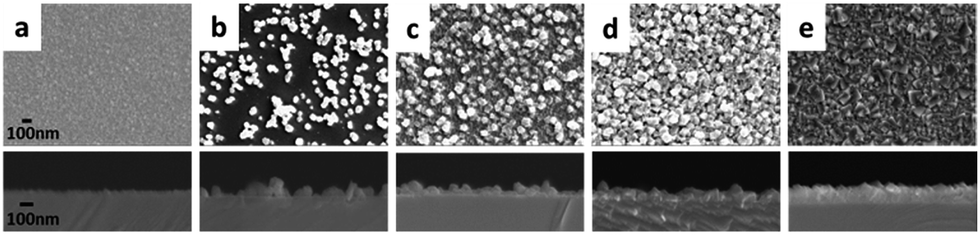 | ||
| Fig. 1 HRSEM plan-view and cross-sectional imaging of PbS(Th) films grown in presence of increasing citrate concentration in solution: (a) 0 mM (b) 4.5 mM (c) 9 mM (d) 22.5 mM (e) 48 mM. Growth conditions were pH = 12.6, T = 55 °C (bath temperature), t = 1.5 h (growth duration). Bath composition was 9 mM lead nitrate, 51 mM TU and 0.1 mM Th4+. Scale bars correspond to the entire row. | ||
X-ray diffractograms were obtained from films grown at increasing bath concentrations of TSC. A correlation between TSC bath concentration and increasing film (111) texturing along with total peak intensity was observed. Representation of the obtained diffractograms (Fig. 2) emphasize these observations, both I(111)/I(200) peak ratio and integrated intensities are increasing as a function of TSC solution concentration.
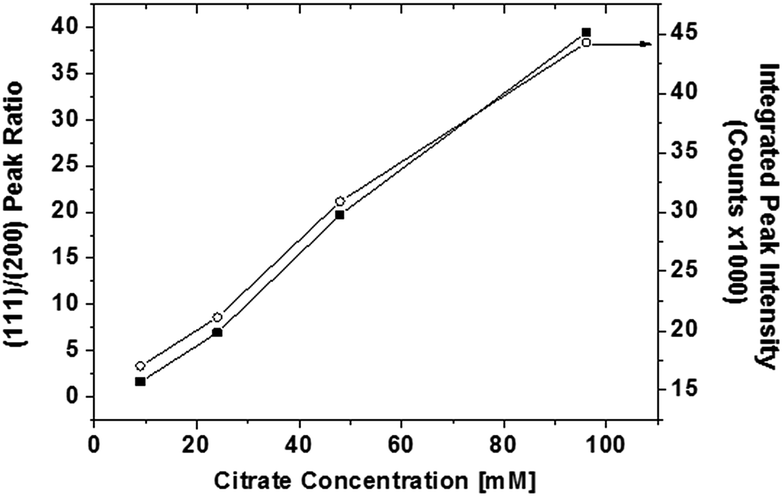 | ||
| Fig. 2 Total integrated XRD peak intensity (open circles, y-axis on the right) and (111)/(200) peak ratio (black squares, y-axis on the left) as a function of citrate concentration. Growth parameters were pH = 12.6, T = 55 °C, t = 1.5 h. Bath composition was 9 mM lead nitrate, 51 mM TU and 0.05 mM Th4+. | ||
Chemical analysis of film composition and distribution was performed by XPS depth profiling. Composition as a function of film depth in a PbS(Th) film grown from a bath containing 0.4 mM Th4+ and 90 mM TSC is presented in Fig. 3a. A uniform distribution of both Th4+ and O2− ions is observed throughout film depth. Comparison was performed by monitoring the composition of a PbS reference film grown using similar conditions except for the presence of Th4+. A uniform distribution of both lead and sulfur were obtained, neither Th4+ nor O2− were present in the reference film (not presented). Depth profiling analysis was repeated for several films grown from solutions containing varying concentrations of TSC. Beyond adsorbed hydrocarbons on the film surface, carbon is not present within the films, indicating that although TSC plays a crucial role in film growth it is absent from the film composition. A uniform distribution of Th4+ was obtained in all cases. Average Th4+ film composition was plotted as a function of bath TSC concentration (Fig. 3b) and a distinct correlation was observed.
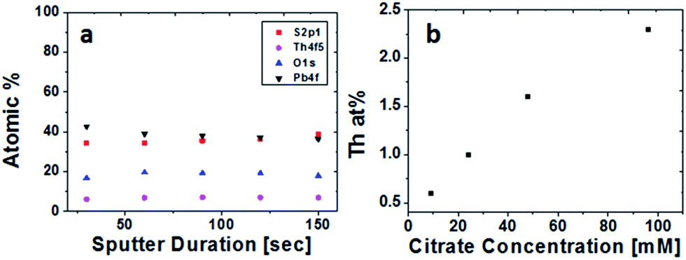 | ||
| Fig. 3 XPS depth profiles of (a) PbS(Th) (b) average Th film composition based on XPS as a function of citrate concentration in the deposition bath. | ||
The chemical environments of Th4+ and O2− in the PbS(Th) films was studied using high resolution XPS (HRXPS). Although no literature data was found on the binding energy of ThS, an increase in binding energy is expected compared to metallic Th values (4f7/2 at 333.0 eV) due to the higher electronegativity of sulfur, but not high enough to be in a fully oxidized state (4f7/2 at 334.5 eV). An increase in binding energy towards 333.5 eV was indeed observed, as seen in Fig. 4a. Monitoring the O spectra revealed two clear bonding states corresponding to Pb–O and ThO2 (Fig. 4b), due to the incorporation of O2− together with Th4+ in the films.
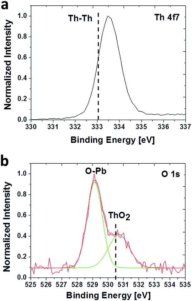 | ||
| Fig. 4 HRXPS spectra acquired from a PbS film containing 9 at% Th. (a) Th 4f7 state and (b) O 1s chemical states. | ||
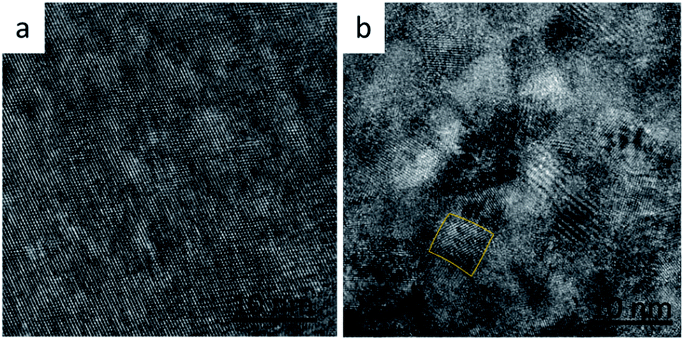
HRTEM and nano-probe EDS studies were performed on several PbS(Th, O) films with varying concentrations of incorporated Th4+, aiming to determine whether Th4+ dissolves in the lattice or it is segregated as a separate phase. STEM EDS elemental line scans combined with HRTEM Fourier transform analysis were performed on film cross sections (Fig. 5a–e). Line scans across several grain boundaries (GB) showed no indication of segregation, but rather, a homogenous distribution of Th4+ and O2− was measured across the films (Fig. SI 1†). An investigation of film microstructure did not reveal nano-precipitates. As seen in Fig. 5c–e, FFT of HRTEM images from different grains within the films shows a single rocksalt PbS phase without overlapping reflections. Additionally, no epitaxial relations between film and substrate were observed, as neighboring grains exhibit different zone axes (Fig. 5d and e).
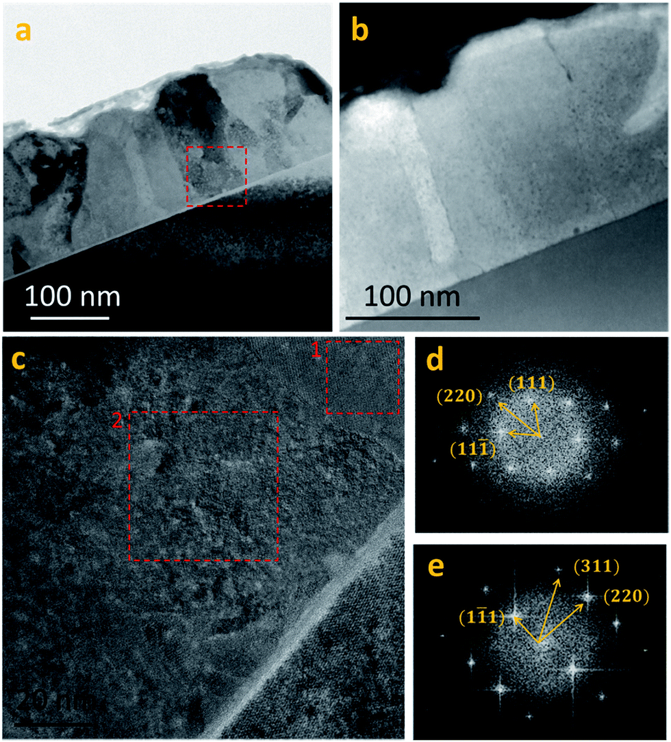 | ||
Fig. 5 (a) X-TEM micrographs of PbS film containing 1 at% Th. (b) HAADF STEM micrograph of the film at the same location. (c) High resolution TEM lattice image taken from the marked region in image (a). (d, e) Fast Fourier Transform (FFT) obtained from the marked regions labeled 1 and 2 in image (c), indicating PbS [1![[1 with combining macron]](https://www.rsc.org/images/entities/char_0031_0304.gif) 0] and [12] zone axes, respectively. 0] and [12] zone axes, respectively. | ||
The optical properties of the films were studied in order to determine whether incorporation of O2− and Th4+ changes the physical properties of the system. Band-to-band radiative recombination was measured as a function of film Th4+ content at both MIR and NIR (Fig. 6a). Unalloyed PbS films emit at 0.43 eV which is in good agreement with the band gap value reported for bulk material. The energy gap (Eg) appears to increase slightly at low Th4+ concentration, up to 2 at%, and notably increases to the NIR above 7 at%.
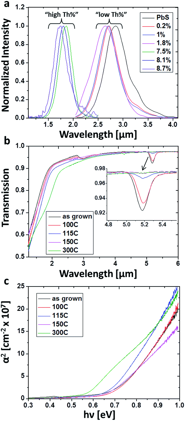 | ||
| Fig. 6 (a) PL spectra of direct band gap emission from PbS films at varying compositions of Th. (b) Transmission measurments performed on PbS(Th, O) films (8.1 at% Th) at various annealing temperatures. Annealing was performed in an inert environment for 3 hours for all samples. Inset at 5.2 μm emphasizes defect state absorption. (c) Tauc plots constructed for the extraction of material band gap. | ||
Thermal treatments were performed in an inert atmosphere for films with high Th4+ concentration (8.1 at% Th). Optical transmission measurements were performed on the films and the absorption coefficients were extracted based upon Beer–Lambert's law.17 Tauc plots were constructed in accordance to direct gap semiconductor behavior (Fig. 6b and c). As-grown films showed a bend in transmission at ∼1.8 μm. By fitting the linear regime in the Tauc plot, the exact value was extracted and found to be 1.75 μm (0.71 eV), in reasonably good agreement with the directly measured PL values (Fig. 6a). Additionally, a clear mid-gap state is seen at ∼5.2 μm, which is attributed to structural defects. Upon thermal treatment, these defects states diminished with increasing temperature and were completely eliminated at 300 °C (Fig. 6b). Monitoring the absorption edge extrapolated from the Tauc plots reveals a decrease in Eg with increasing annealing temperature, beginning at 0.71 eV for untreated films, 0.71 eV, 0.68 eV, 0.66 eV and 0.57 eV for films treated at 100 °C, 115 °C, 150 °C and 300 °C correspondingly (Fig. 6c).
Discussion
In the alkaline aqueous environment, Th4+ and hydroxide ions form a low solubility complex (Ksp = 10−44.7), thus limiting the availability of Th4+ ions that can incorporate into the deposited PbS films.18 Therefore, lowering of the solution pH should result in an increase in concentration of free Th4+. Growth of PbS(Th) thin films was achieved here using the CBD technique at a substantially lower pH value. Nevertheless, varying the solution pH from 13.3 to 12.8 has resulted in decreased film thickness by an order of magnitude (from ∼300 nm to ∼30 nm). This effect was previously reported for the PbS||GaAs system and was attributed to slower thiourea decomposition with decreasing pH (and hence, less availability of sulphide ions in the sulphide limited regime), although it did not have such a drastic effect.6 In the current PbS(Th) system, Th4+ competes with lead cations over complexation ions. Uncomplexed Pb2+ cations react with sulphide anions to rapidly precipitate in the solution; moreover, tetra-valent Th4+ ions having an exceptionally high affinity toward hydroxides further lower the effective pH, thus, further inhibiting sulphide release via thiourea decomposition. Another point to consider is the incorporation of Th4+ ions in the growing PbS film. Addition of Th4+, which have different ionic radius and valency compared to lead ions, are likely to present a perturbation to the PbS lattice. Thus, the low film thickness reported here is presumably due to a combination of the effects mentioned above (Fig. 1a). TSC has been reported to perform as a strong complexing agent of Th4+ cations in the presence of alkaline solutions, forming the stable Th(OH)2cit24− complex, thus, freeing hydroxide ions required for the thiourea decomposition reaction.13,14 This behavior is presented in Fig. 1b–e where increasing citrate concentration in solution results in a more compact film; moreover, a transition from cluster to IBI growth mechanism can be seen here, which again points to the availability of complexing agents.The increase in XRD total peak area as a function of TSC bath concentration is attributed to both increasing film thickness and apparent compactness, which are both a direct result of available hydroxide ions in solution. As mentioned, PbS(Th) films with 〈111〉 texture and triangular pyramidal surface topography were reported by Biton et al. as a result of Th4+ introduction into chemically deposited PbS thin films.15 Similar behavior was observed here as a function of increasing TSC bath concentration, as change occurs from non-textured films towards strong (111) texturing (Fig. 2). Change in film texturing with increasing TSC concentration (Fig. 2) was suspected to result from increasing Th4+ film content. This was verified by XPS analysis, revealing the direct correlation between increasing TSC solution concentration and Th4+ film composition (Fig. 3b). By preventing formation of the low solubility Th(OH)4 products, complexation of Th4+ ions by TSC appears to have a key enabling role in the formation of Th alloyed PbS thin films with relatively high Th concentrations. As seen in Fig. 3a and b, a uniform distribution of Th4+ throughout the film was achieved, which is accompanied by incorporation of oxygen. Note that although relatively large percentages of O2− and Th4+ are present in the films (up to 9 at% Th and 20 at% O), no additional crystalline phases are found; diffractograms obtained from PbS(Th, O) films confirm a single phase of PbS present (ICDD#05-0592, Fig. SI 2†),19 suggesting that O2− and Th4+ are uniformly dissolved in the PbS matrix. Additionally, no clear trend of XRD peak position shifts (typical to alloyed films) was observed with increasing Th4+ and O2− film composition. The lattice parameters of PbS and of the cubic rocksalt phase of ThS are quite similar (5.936 Å and 5.682 Å, respectively), therefore a noticeable shift in XRD peak positions will likely occur only at sufficiently high concentrations of Th4+. A rough estimation of the minimal amount of Th4+ which would result in an observable peak shifting (0.07° in 2θ; twice the step resolution) was calculated. According to Bragg's law such a shift would account for a change of ∼0.017 Å in the lattice parameter. Implementing this change in lattice parameter according to Vegard's law
| aPbS(Th) = aThSx + aPbS(1 − x) |
leads to a minimum requirement of ∼7 at% Th for observable peak shifting. This explains why no XRD peak shifting was observed for the varying Th4+ concentrations used in this work.
To quantify the behavior of oxygen accompanying Th incorporation, average film compositions were analyzed by XPS depth profiles and plotted as a function of Th film concentration (Fig. 7a–c). Evidently, incorporation of Th4+ is accompanied by decreasing lead and sulphide ions and a stronger increase in O2−, where incorporation of each Th4+ cation is accompanied by roughly two O2− anions. This is quite expected considering that Th(OH)22+ ions are readily formed in the alkaline solution, although polymerization of these ions in solution was reported to be inhibited by citrate by attaching Th(OH)22+ ions to a complex of 2 or 3 citrate molecules.14 Incorporation in the lattice may occur through surface reaction of incipient Th-complex and S2− dangling bonds in the growing films. If Th4+ ions are dissolved in the lattice, it is likely to occur via substitution of Pb2+ lattice sites and charge compensation by means of interstitial O2− anions or OH− anions incorporation of OH− anions is more likely to occur, in terms of charge compensation, as will be shown later in discussion. Contrary to this assumption, O2− (or OH−) and Th4+ might be segregated at GB or present as ThO2 nano sized precipitates, which were reported to readily form in alkaline solutions with a typical size of ∼4 nm.18 Such a scenario will present a quite similar XPS spectrum, and is not expected to appear in the diffractograms as separate phases, due to small size or amorphous nature of the segregating phases. However, careful analysis performed on X-TEM micrographs taken from films with varying concentrations of Th4+ did not show any such nano precipitates neither within the lattice nor in GB. This result, combined with the uniform distribution of both Th4+ and O2− (or OH−) throughout the films, as measured using EDS line scans in STEM mode, strongly suggests that Th4+ and accompanying O2− (or OH−) ions are fully dissolved in the PbS lattice. Moreover, the same composition trends which were observed in the XPS composition analysis (Fig. 7) were reaffirmed in the EDS measurements.
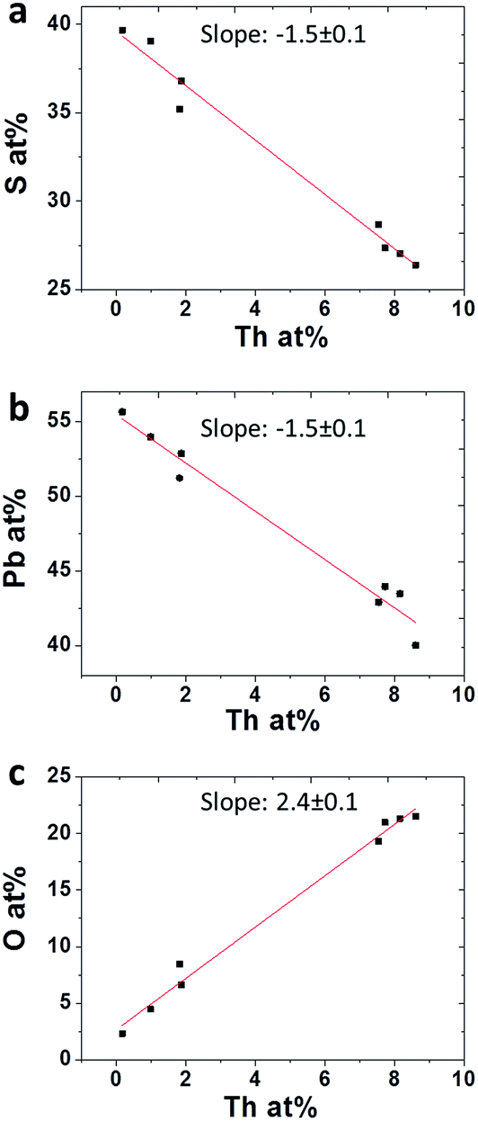 | ||
| Fig. 7 Average concentrations obtained using XPS for (a) S (b) Pb and (c) O in PbS(Th) films as a function of Th concentration. | ||
Considering concentration dependencies presented in Fig. 7, for every two Th4+ ions incorporated within the film, three Pb2+ and S2− ions are omitted, and five O2− ions are introduced.
The assumption that only O2− ions dissolve in the lattice together with Th4+ ions does not account for charge neutrality in the films. However, considering that Th4+ ions are bonded to hydroxides throughout the deposition, the more likely scenario which accounts for film charge neutrality is the incorporation of Th(OH)22+ ions. Preliminary Atom Probe Tomography (APT) analysis performed on PbS(Th) films support this hypothesis as presence of hydroxides was observed throughout the films. Based on the reported data, a charge compensation mechanisms describing Th4+ lattice incorporation in the PbS films are currently being addressed by applying density function theory together with APT investigations (which is sensitive to OH− ions) and will be published in the future.
The transition to (111) texture upon incorporation of Th4+ in the films remains an open question. In the rocksalt structure, the (100) surface typically has a lower surface energy and hence, development of (100) facets favor the formation of cube-shaped PbS crystals. Once Th4+ is introduced, there is an apparent transition to energetically preferable (111) planes. This point is strengthened by the fact that the films are not in epitaxial relations with the GaAs substrate, and the preferred (111) texturing is a result of growing crystallites exposing the energetically stable surface planes. To verify this hypothesis PbS and PbS(Th, O) films were grown on glass substrates and analyzed with XRD (Fig. SI 2†). PbS diffractograms indeed show the powder peak intensity ratios, as amorphous substrates do not dictate preferred orientation on the incipient films. Contrarily, PbS(Th, O) films present (111) texturing, supporting the findings that this effect is phase correlated and not a result of epitaxial relations with the substrate. In line with these arguments is the fact that epitaxial monocrystalline PbS thin films on GaAs showed a (110) orientation rather than the naturally expected (100) orientation, most likely due to interfacial stresses in the early stages of growth.4,12
For many binary alloys, AxB1−x, Eg changes linearly with x.20,21 However, plotting the optical band gap as a function of Th4+ concentration in the films presents two distinct regimes (Fig. 8).
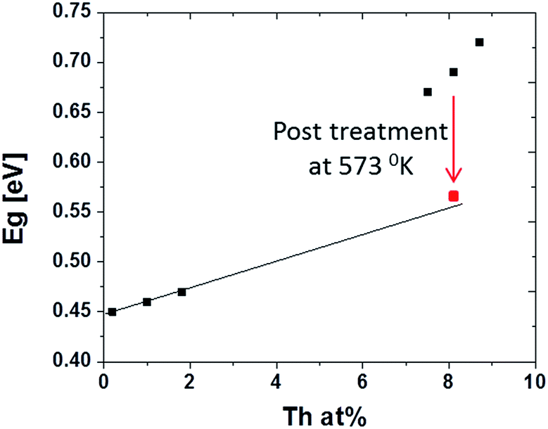 | ||
| Fig. 8 PbS(Th, O) optical band gap plotted as a function of Th4+ film concentration as obtained through XPS analysis. Red square corresponds to 8.1 at% Th sample after annealing at 573 K for 180 min. | ||
In ternary semiconductors a deviation from linear behaviour of Egversus composition is termed the bowing effect, which results from both chemical and size variation contributions in the system. Interstitial and substitution ions causing changes in unit cell volume are considered size variations. Changes in chemical bonds, which effect the periodic potential due to variations in electronic configurations of exchanged atoms, are considered chemical variations.22,23 Chemical variations are likely to exist for PbS(Th, O), as shown above for both O2− and Th4+, but size effects should not contribute, since there is no indication of lattice parameter increase (verified through XRD). Regardless, it appears that bowing is still occurring in the PbS(Th, O) system, indicating that another physical property is changing in the films along with the chemical variations. A closer examination of film microstructures reveals formation of sub-domains within the film grains at high Th4+ concentrations, an effect which is not observed at low concentrations (Fig. 9a and b). Bright field TEM micrographs depicting average film grain size of ∼50 nm confirm the described sub-domain microstructure (in contrast to nanocrystalline films) and are presented in Fig. SI 3.† Increasing Th4+ concentration in the films results in local lattice strain, once the strain value exceeds a critical limit, it is partially relaxed by the formation of GB, resulting in the observed sub-domain microstructure. Thus, a combination of an inherently large Bohr radius and increased confinement due to formation of sub-domain boundaries contributes to increased Eg at high Th concentrations.
 | ||
| Fig. 9 HRTEM lattice images of PbS(Th, O) film cross sections with a composition of (a) 1 at% Th and (b) 8.1 at% Th. The marked region presents an example for a sub-domain. | ||
To verify this hypothesis, thermal treatments were performed, in an inert atmosphere, to high Th4+ concentration films (8.1 at% Th). If the variation in Eg results from sub-domain formation, then by introducing thermal energy, grain coarsening should occur, resulting in Eg red-shifting. As-grown films transmission spectra show a clear mid-gap state is at ∼5.2 μm, which is attributed to structural defects. Theoretical studies recently reported that Schottky pair defects can give rise to distinct defects states at 0.23 eV (5.4 μm) above the valance band edge of PbS.24 These defects were predicted to participate in radiative recombination, supporting the assignment of the 5.2 μm mid-gap states experimentally observed in this work as defect states.24 To the best of our knowledge this is the first empirical evidence for these theoretically predicted defect states. Upon thermal treatment, these defects states diminished with increasing temperature and were completely eliminated upon treatment at 300 °C for 3 hours (Fig. 6b). This behaviour emphasizes absorption resulting from structural defects, which begin migration and annihilation once sufficient thermal energy is provided. Once the films were sufficiently thermally treated to remove absorbing defect states, the band gap red shifts noticeably and the dependency on Th4+ concentration acts according to Vegard's law, i.e., a linear increase of band edge with increasing Th4+ concentration (Fig. 8).
Conclusions
In summary, Th-alloyed lead sulphide thin films were successfully grown using CBD with varying concentrations of Th up to ∼9 at%. TSC was shown to play a crucial role as co-complexant, enabling the decrease of pH, which would otherwise inhibit Th4+ incorporation. Increasing TSC concentration led to increasing Th4+ and accompanying O2− film compositions which, in turn, altered film texturing from (100) towards (111). Conclusive evidence was presented regarding the miscibility of Th4+ and O2− within the PbS phase. Control over the concentration of Th4+ in PbS films was demonstrated and viable mechanisms for incorporation were presented. Optical properties were investigated as a function of Th4+ composition in the films, revealing bowing behaviour in the dependency of the optical band gap on film Th4+ concentration. Examination of film microstructures revealed the formation of nanoscale sub-domains at high Th4+ concentrations that may lead to quantum confining effects and the observed bowing behaviour. Furthermore, mid-gap defect state absorption was noticeable in as grown high concentration films. Upon thermal treatment, these absorbing states diminished until completely eliminated once treated at 300 °C for 3 hours. A correlation was observed between film band gap and structural defects, as red-shifting in Eg values occurs once thermal treatments were applied, diminishing the observed bowing effect. The ability to tune the optical band gap by controlling film composition provides additional means of control for future use in advanced optoelectronic applications. By replacing the stable 232Th with the active 228Th isotope using similar growth conditions, PbS(Th, O) thin films also present a promising candidate for self-irradiation damage studies, without the use of special facilities for fabrication and handling of radioactive alpha-emitting samples.Acknowledgements
Expert assistance from Dr N. Froumin (XPS), Dr D. Mogilyanski (XRD) and Dr S. Hazan (FTIR) is gratefully acknowledged. This work has been partially supported by the Pazy Foundation, the FTA program of the Israeli National Nanotechnology Initiative, and by the Israel Science Foundation under Grant no. 156/14.References
- G. Hodes, Chemical Solution Deposition of Semiconductor Films, Marcel Dekker, Inc., NJ, USA, 2002 Search PubMed.
- M. Shandalov and Y. Golan, Eur. Phys. J.: Appl. Phys., 2003, 24, 13–20 CrossRef CAS.
- M. Shandalov and Y. Golan, Chem. Mater., 2006, 18, 3593–3595 CrossRef CAS.
- A. Osherov and Y. Golan, MRS Bull., 2010, 35, 790–796 CrossRef CAS.
- T. Templeman, M. Biton, T. Safrani, M. Shandalov, E. Yahel and Y. Golan, CrystEngComm, 2014, 16, 10553–10559 RSC.
- A. Osherov, V. Ezersky and Y. Golan, J. Cryst. Growth, 2007, 308, 334–339 CrossRef CAS.
- P. K. Nair and M. T. S. Nair, J. Phys. D: Appl. Phys., 1990, 23, 150–155 CrossRef CAS.
- T. Safrani, T. A. Kumar, M. Klebanov, N. Arad-Vosk, R. Beach, A. Sa'ar, I. Abdulhalim, G. Sarusi and Y. Golan, J. Mater. Chem. C, 2014, 2, 9132–9140 RSC.
- S. M. Pawar, B. S. Pawar, J. H. Kim, O. Joo and C. D. Lokhande, Curr. Appl. Phys., 2011, 11, 117–161 CrossRef.
- A. Osherov, J. P. Makai, J. Balazs, Z. J. Horvath, N. Gutman, A. Sa'ar and Y. Golan, J. Phys.: Condens. Matter, 2010, 22, 262002 CrossRef PubMed.
- S. Sengupta, M. Perez, A. Rabkin and Y. Golan, CrystEngComm, 2016, 18, 149–156 RSC.
- A. Osherov, M. Shandalov, V. Ezersky and Y. Golan, J. Cryst. Growth, 2007, 304, 169–178 CrossRef CAS.
- D. P. Raymond, J. R. Duffield and D. R. Williams, Inorg. Chim. Acta, 1987, 140, 309–313 CrossRef CAS.
- A. R. Felmy, H. Cho, D. A. Dixon, Y. Xia, N. J. Hess and Z. Wang, Radiochim. Acta, 2006, 94, 205–212 CrossRef CAS.
- M. Biton, A. Shamir, M. Shandalov, N. Arad-Vosk, A. Sa'ar, E. Yahel and Y. Golan, Thin Solid Films, 2014, 556, 223–229 CrossRef CAS.
- A. Osherov, V. Ezersky and Y. Golan, Eur. Phys. J.: Appl. Phys., 2007, 37, 39–47 CrossRef CAS.
- S. Gorer, A. Albu-Yaron and G. Hodes, J. Phys. Chem., 1995, 99, 16442–16448 CrossRef CAS.
- J. J. Katz, L. R. Morss, N. M. Edelstein and J. Fuger, The Chemistry of the Actinide and Transactinide Elements, Springer, Netherlands, 3rd edn, 2008, vol. 1–5 Search PubMed.
- H. E. Swanson, Standard X-ray diffraction powder patterns, U.S. Dept. of Commerce, National Bureau of Standards, Washington, DC, 1953 Search PubMed.
- L. Zhang, L. Li, L. Wang, M. Li, Y. Lu, B. K. Meyer and Y. He, J. Alloys Compd., 2014, 617, 413–417 CrossRef CAS.
- R. A. Soref and C. H. Perry, J. Appl. Phys., 1991, 69, 539–541 CrossRef CAS.
- I. Gorczyca, T. Suski, N. E. Christensen and A. Svane, Phys. Rev. B: Condens. Matter, 2011, 83, 153301 CrossRef.
- J. E. Jaffe and A. Zunger, Phys. Rev. B: Condens. Matter, 1984, 29, 1882–1906 CrossRef CAS.
- W.-F. Li, C.-M. Fang, M. Dijkstra and M. A. van Huis, J. Phys.: Condens. Matter, 2015, 27, 355801 CrossRef PubMed.
Footnote |
| † Electronic supplementary information (ESI) available. See DOI: 10.1039/c6ra21188g |
| This journal is © The Royal Society of Chemistry 2016 |