
 Open Access Article
 This Open Access Article is licensed under a
 Creative Commons Attribution 3.0 Unported Licence
Promising field electron emission performance of vertically aligned one dimensional (1D) brookite (β) TiO2 nanorods
Rupesh S.
Devan
 *ab,
Yuan-Ron
Ma
*c,
Mahendra A.
More
*b,
Ruchita T.
Khare
b,
Vivek V.
Antad
d,
Ranjit A.
Patil
c,
Vishal P.
Thakare
be,
Rajendra S.
Dhayal
f and
Lukas
Schmidt-Mende
g
*ab,
Yuan-Ron
Ma
*c,
Mahendra A.
More
*b,
Ruchita T.
Khare
b,
Vivek V.
Antad
d,
Ranjit A.
Patil
c,
Vishal P.
Thakare
be,
Rajendra S.
Dhayal
f and
Lukas
Schmidt-Mende
g
aCentre for Physical Sciences, School of Basics and Applied Sciences, Central University of Punjab, Bathinda, 151001, India. E-mail: devan_rs@yahoo.co.in
bDepartment of Physics, Savitribai Phule Pune University, (Formerly, University of Pune), Pune 411007, India. E-mail: mam@physics.unipune.ac.in
cDepartment of Physics, National Dong Hwa University, Hualien 97401, Taiwan, Republic of China. E-mail: ronma@mail.ndhu.edu.tw
dNowrosjee Wadia College of Arts & Science, 19, Late Prin. V. K. Joag Path, Pune 411001, India
ePhysical & Materials Chemistry Division, CSIR-National Chemical Laboratory, Dr Homi Bhabha Road, Pune 411008, India
fCentre for Chemical Sciences, School of Basics and Applied Sciences, Central University of Punjab, Bathinda, 151001, India
gDepartment of Physics, University of Konstanz, Constance 78457, Germany
First published on 10th October 2016
Abstract
We evidence field-electron emission (FE) studies on the large-area array of one-dimensional (1D) brookite (β) TiO2 nanorods. The pure 1D β-TiO2 nanorods of 10 nm width and 760 nm long were synthesized on Si substrate utilizing hot-filament metal vapor deposition technique. X-ray diffraction (XRD) and transmission electron microscopy (TEM) analysis evidenced the β-TiO2 nanorods to be composed of orthorhombic crystals in brookite (β) phase. X-ray photoemission spectroscopy (XPS) revealed the formation of pure stoichiometric (i.e. 1![[thin space (1/6-em)]](https://www.rsc.org/images/entities/char_2009.gif) :1.98) 1D TiO2 nanorods. The values of turn-on field, required to draw current density of 10 μA cm−2, was observed 3.9 V μm−1 for pristine 1D β-TiO2 nanorods emitters, which were found significantly lower than doped/undoped 1D TiO2 nanostructures (i.e. nanotubes, nanowires, nanorods) based field emitters. The enhanced FE behavior of the TiO2/Si emitter can be attributed to modulation of electronic properties due to the high aspect ratio of vertically aligned TiO2 nanorods. Furthermore, the orthodox emission situation of pristine TiO2/Si emitters exhibit good emission stability and reveal their potentials as promising FE material.
:1.98) 1D TiO2 nanorods. The values of turn-on field, required to draw current density of 10 μA cm−2, was observed 3.9 V μm−1 for pristine 1D β-TiO2 nanorods emitters, which were found significantly lower than doped/undoped 1D TiO2 nanostructures (i.e. nanotubes, nanowires, nanorods) based field emitters. The enhanced FE behavior of the TiO2/Si emitter can be attributed to modulation of electronic properties due to the high aspect ratio of vertically aligned TiO2 nanorods. Furthermore, the orthodox emission situation of pristine TiO2/Si emitters exhibit good emission stability and reveal their potentials as promising FE material.
Introductions
The one-dimensional (1D) nanostructure morphologies of transition metal oxides offer the advantages of a high aspect ratio, sharp tip features, good stability, and oxidation resistance,1 which are prerequisites to enhance the field emission (FE) properties and develop efficient functional devices. Among the various 1D metal-oxides, TiO2 is one of the most fascinating functional materials. It has received considerable attention for applications in solar cell,2 photocatalysis,3 electrochromic displays,4 supercapacitors,5 and batteries,6etc., owing to its non-toxicity, abundance, and good chemical and thermal stability. The FE properties of TiO2 are rather explored in spite of its low work function range (3.9 to 4.5 eV) than other popular metal-oxides, owing to its availability in limited morphological forms.6 The geometrical similarity of TiO2 nanotubes with carbon nanotubes influenced many researchers to explore the FE characteristics of TiO2 nanotubes7–10 and nanotubes with sharp tips.11 However, the reproducibility of the TiO2 nanotubes remained challenging. Not only the diameter influence the FE performance, but the density (i.e. separation between nanotubes) and clusters appearance of the TiO2 nanotubes array appear to create field screening effects.7 Moreover, the uncontrolled and random dispersion of TiO2 nanowires12 and nanorods13 affect their FE adversely. Highly dense rutile TiO2 hierarchical nanorods network arranged in the form of dandelion flower like morphology suffer from significant field screening effect thereby exhibiting poorer FE behavior.14 On the contrary, the influence of oxygen vacancies on the electron affinity alter the electronic structure of TiO2 and thereof FE properties.15 Therefore, the doping of 1D TiO2 nanostructures with N,9 Fe,16 and C,17etc. was seldom adopted to enhance the FE characteristics.Theoretical analysis and experimental studies have proved the advantage of brookite (β) phase over anatase and rutile phase of TiO2. Mo et al.18 have reported electronic and optical properties of three different polymorphs (rutile, anatase, and brookite) of TiO2. They used first-principles orthogonalized linear combinations of atomic orbitals (OLCAO) method to calculate the electronic structure of TiO2 and reported that the brookite phase has a much larger static dielectric constant of 7.89 compared to that of rutile (6.62) and anatase (6.04) phase. Furthermore, comparably better photoactivity is observed in brookite TiO2 thin films/nanoparticles than the anatase and rutile.19,20 Shibata et al.21 found brookite TiO2 nanoparticles as excellent coating materials because of its better photoinduced hydrophilicity than anatase one. Koelsch et al.22 reported better photovoltaic abilities of brookite TiO2 nanoparticles over anatase phase in terms of bandgap and electrochemical characterization in water and acetonitrile. Furthermore, our detailed report on excellent electrochromic properties with 99% reversibility4 and highly stable supercapacitive performance with long cycle lifetime (10000 cycles) of brookite TiO2 nanoneedles5 corroborate significant electronics advantages of the brookite phase over the anatase and rutile phase. However, the brookite consisting of distorted TiO6 octahedra is less investigated. The synthesis of pure brookite phase is always challenging due to its metastable nature23 and commonly accompanied with the anatase and/or rutile phases.3,24,25 That is why numerous scientific reports are found on the utilization of rutile and anatase phases for variety of applications including field emitters.10–12,26,27 High temperature calcinations25 and annealing24 processes were unsuccessful to yield pure brookite phase. Nevertheless, β-phase is thermodynamically most stable in nanocrystalline form at dimensions between 11–35 nm.3 Despite the facts above, to the best of our knowledge, there is no study report on FE performance of 1D β-TiO2 nanorods. Therefore, for promising FE behavior, it is of scientific and technological importance to growing vertically aligned 1D β-TiO2 nanorods.
In this work, we present 1D β-TiO2 nanorods arrays as promising field-emitters. The large area arrays of vertically aligned TiO2 nanorods of brookite phase were synthesized using hot-filament metal vapor deposition (HF-MVD) technique, which is unique and simple technique to provide diverse nanostructures morphologies.28–33 The structural morphology, size distribution, electronic structure, and chemical composition of as-synthesized large-area arrays β-TiO2 nanorods was examined utilizing various techniques such as X-ray photoemission spectroscopy (XPS), field-emission scanning electron microscopy (FESEM), transmission electron microscope (TEM), and X-ray diffractometer (XRD), etc. Interestingly, the vertically aligned and uniformly distributed 1D β-TiO2 nanorods array exhibit low turn-on field, good emission stability, and large field enhancement factor.
Experimental
Large area arrays of TiO2 nanorods were synthesized using hot-filament metal vapor deposition (HFMVD) technique. A clean titanium (Ti) wire (99.9% pure) of a diameter of 1 mm, passed through a pure graphite disc was fixed on two supporting Cu electrodes in a vacuum chamber. Once the pressure of the vacuum chamber was pumped down to 1.3 × 10⁻² mbar, the Ti wire was heated to ∼1300 °C for 25 min to generate controlled hot titanium vapor. The hot titanium vapor encountered and reacted with the residual oxygen (or leaking air) to form a metal-oxide vapor of TiOx (x ≤ 2). TiOx vapors meet rather cold Si wafers (substrate) which had been placed on the graphite disc holder (∼3 mm above the Ti wire) and condensed into one-dimensional (1D) TiO2 nanorods. After that, the surface morphology of the as-synthesized large-area arrays of β-TiO2 nanorods was characterized using a field emission scanning electron microscope (FESEM, JEOL JSM-6500F). The crystal structure of β-TiO2 nanorods was confirmed with an X-ray diffractometer (Philips X'Pert PRO) with Cu-Kα radiations (λ = 1.541 Å). Structural analysis of β-TiO2 nanorods was carried out using a transmission electron microscope (TEM, JEOL, JEM-2100) with a selected-area electron diffractometer (SAED) at an accelerating voltage of 200 kV. The band-structure and chemical states present in as-synthesized β-TiO2 nanorods was analyzed using X-ray photoelectron spectrometer (XPS, Thermo Scientific Inc. K-alpha) with a microfocus monochromated Al Kα X-ray. The individual FE studies of the TiO2 nanorods were carried out in a vacuum chamber at a base pressure of ∼10 × 10−9 mbar. The semitransparent phosphor screen as an anode was maintained at an optimized distance from specimen/samples of β-TiO2 nanorods. Moreover, to avoid the effect of contamination, preconditioning of the samples was carried out by applying a voltage of ∼3 kV for 30 min. The FE current (I) was measured with an electrometer (Keithley 6514) at dc voltage (V) applied using high voltage DC power supply (0–40 kV, Spellman, U.S.). The long-term stability of the FE current was recorded for the TiO2 nanorods.Results and discussion
The surface morphology in FESEM images (Fig. 1) reveals the formation of uniformly distributed and vertically aligned TiO2 nanorods on Si substrate. Uniformly distributed TiO2 nanorods over a large area (Fig. 1(a)) signifies variation in their diameters (inset of Fig. 1(a)), which were confined to the very limited range and all are smaller than 20 nm. The array contains ∼2550 nanorods per square micrometer. The high magnification tilted view (Fig. 1(b)) of TiO2 nanorods recorded at a tilt angle of 35° to the surface normal direction shows vertically standing and well separated nanorods with their clearly visible textural boundaries. The high magnification FESEM image in Fig. 1(c) shows a side view of the TiO2 nanorods array with an average length of ∼760 nm. This indicates that no distinct thin layer of SiO2 or TiO2 nanoparticles has formed before the growth of the TiO2 nanorods even after a high temperature of the Ti source (1300 °C). A statistical histogram of the diameter distribution (Fig. 1(d)) illustrates that the diameter of the TiO2 nanorods falls in the range of 5 to 20 nm. Most of the TiO2 nanorods have a diameter of about ∼10 nm. This distribution of varying diameters can be fitted to a log-normal distribution function as, | (1) |
![[d with combining macron]](https://www.rsc.org/images/entities/i_char_0064_0304.gif) [≡ 10.81 ± 0.13 nm] is the mean (average) diameter of various nanorods; A [≡ 93.65 ± 4.93] is the normalization constant; and σ [≡ 0.21 ± 0.01] is the standard deviation of diameters of nanorods. The log-normal distribution of diameters of the nanorods is asymmetrical. The small standard deviation (σ ≤ 0.25) of the diameter distribution indicates that the nanorods are well confined to a limited diameter range.
[≡ 10.81 ± 0.13 nm] is the mean (average) diameter of various nanorods; A [≡ 93.65 ± 4.93] is the normalization constant; and σ [≡ 0.21 ± 0.01] is the standard deviation of diameters of nanorods. The log-normal distribution of diameters of the nanorods is asymmetrical. The small standard deviation (σ ≤ 0.25) of the diameter distribution indicates that the nanorods are well confined to a limited diameter range.
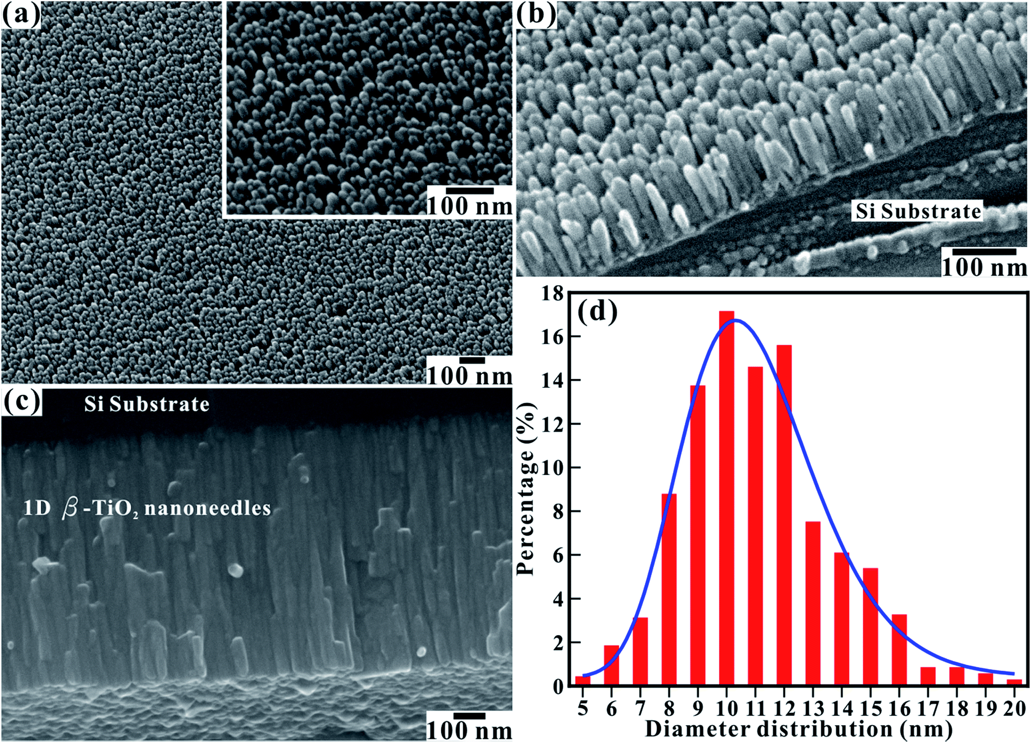 | ||
| Fig. 1 FESEM image showing the (a) top, (b) tilted, and (c) side views of the large-area array of vertically aligned 1D TiO2 nanorods on Si substrate. Inset of (a) shows high-magnification FESEM image of the 1D TiO2 nanorods. The tilted view was recorded at a tilt angle of 35° to the surface normal direction. (d) Statistical histogram of the diameter distribution of the TiO2 nanorods fitted by a log-normal distribution function. | ||
XRD pattern is used as a fingerprint to identify the crystalline structure of the TiO2 nanorods. The room temperature XRD pattern of as-synthesized TiO2 nanorods arrays (Fig. 2(a)) exhibits a sets of well-defined diffraction peaks (indicated by β) at 2θ values of 32.4, 37.1, 38.8, 44.8, 45.5, 46.2, 52.3, 52.9, 55.6, 57.9, 75.6, 76.6, and 77.8, respectively, are indexed to the (020), (021), (121), (212), (302), (411), (420), (222), (511), (322), (531), (432), and (423) lattice planes of orthorhombic crystals of TiO2 in brookite (β) phase, assigned to the space group Pbca (JCPDS – 761936) with lattice constants of a = 0.919 nm, b = 0.546 nm, c = 0.516 nm and α = β = γ = 90°. The remaining diffraction peaks (indicated by asterisks) represents the Si substrate in cubic crystalline form of the space group P213 with lattice contacts a = b = c = 7.16 nm, and α = β = γ = 90° (JCPDS – 850621). Further, the crystalline structure of β-TiO2 nanorods was confirmed by selected area electron diffraction (SAED) pattern (Fig. 2(b)) of a β-TiO2 nanorod extracted from large area array. The SAED pattern was collected from the portion of the β-TiO2 nanorod shown in the inset of Fig. 2(b), which evidenced four-fold symmetric diffraction spots indexed to the [101] zone axis. The indexing of the reflections in the SAED pattern is well consistent with the XRD analysis discussed above. This clearly evidenced that the β-TiO2 nanorods were indeed composed of orthorhombic crystals in brookite (β) phase. Most of the phase transformation results suggest that thermodynamic phase stability for the three polymorphs of TiO2 is rutile > brookite > anatase. Kominami et al.25 reported that anatase is thermodynamically stable at crystalline dimensions below 11 nm, brookite is most stable for dimensions between 11–35 nm, and rutile is stable above the 35 nm. Therefore, decisive synthesis parameters (i.e. temperature, time and pressure) of the HFMVD technique were optimized to achieve the diameter of TiO2 nanorods below 35 nm. Therefore, dimensions of nanorods (i.e. <20 nm) observed in this study ruled out the possibility of formation of rutile phase. The synthesis process involving additional reactants such as water and acid/base medium assists the faster nucleation process than the growth of the morphology (e.g. 1D or 0D) favor for the formation of anatase phase.8,9,11,17,34,35 Furthermore, faster nucleation process than the growth leads to the lower size morphologies. Synthesis of TiO2 nanorods is carried out by heating Ti-metal filament at a higher temperature in the absence of additional reactants. Consequently, the formation of β-TiO2 nanorods is observed, and other phases such as anatase and rutile have been precluded.
 | ||
| Fig. 2 (a) XRD pattern of a large area array of the 1D TiO2 nanorods on Si-substrate, (b) SAED pattern collected from a single 1D TiO2 nanorod shows diffraction spots indexed to the [101] zone axis of brookite crystal structure. Inset of (b) shows TEM image of single 1D TiO2 nanorod extracted from the large area array. | ||
XPS studies were carried out for the quantitative analysis of the electronic structure and chemical properties of β-TiO2 nanorods. To precisely determine the features of the double peaks of Ti (2p3/2) and Ti (2p1/2), the Ti (2p) XPS spectra was decomposed via Voigt curve fitting within the Shirley background (Fig. 3(a)). The perfect fit for two peaks located at binding energies (BE) of 458.98 and 464.60 eV, respectively, corresponds to the Ti (2p3/2) and Ti (2p1/2) core levels of Ti4+ cations and not of Ti3+.36,37 The energy separation of 5.62 eV between Ti (2p3/2) and Ti (2p1/2) peaks and their area ratio of 2.49 reflects a strong bonding between Ti and O atoms. The full width at half maximum (FWHM) of the Ti (2p3/2) and Ti (2p1/2) peak are 1.32 and 2.22, respectively, indicative of the high resolution of the Ti (2p) XPS spectrum in comparison with previous studies.37,38 Similarly, O (1s) XPS spectra of nanorods was decomposed via Voigt curve fitting within the Shirley background (Fig. 3(b)). The results demonstrate the perfect fits to two peaks located at 530.16 and 531.53 eV, with FWHM's of 1.42 and 2.22 eV, respectively. The lower BE peak at 530.14 eV corresponds to the O (1s) core level of the O2− anions in β-TiO2 nanorods. However, higher BE at 531.53 eV is ascribed to surface contamination, such as carbon oxides or hydroxides.39–41 The O (1s) peak observed at BE of 530.16 eV, is associated with the Ti–O chemical bonding (OTi–O1s).36 The atomic ratio of oxygen and titanium (i.e. O/Ti) estimated by integrating the area beneath the decomposed peaks of O (1s) and Ti (2p3/2) is ∼1.98 (i.e. Ti:O = 1:1.98), which is very close to the stoichiometric ratio (i.e. 1:2) of pure TiO2. This confirms that all nanorods in the large area array are fully oxidized, and composed of pure stoichiometric TiO2 only and no titanium suboxides (TiOx). Moreover, the BE difference (ΔE) of 71.18 eV between O (1s) and Ti (2p3/2) peaks is very close to that of 71.5 eV for TiO2, and significantly smaller than that of 73.4 eV for Ti2O3 and 75.0 eV for TiO.42 This confirms again that, nanorods array is formed of pure stoichiometric TiO2.
 | ||
| Fig. 3 Typical high-resolution XPS spectra of the (a) Ti (2p) and (b) O (1s) core levels of the large area array of 1D β-TiO2 nanorods. The XPS spectra were decomposed via Voigt curve function fitting. | ||
FE measurements of pristine β-TiO2 nanorods (≡ 1D β-TiO2/Si) were performed in a planar diode configuration. The macroscopic area of the emitting device was ∼0.30 cm2, and values of the anode–cathode separation used were 500, 1000, 1500 and 2000 μm. The variation in the macroscopic electron emission current density (J) as a function of applied electric field (E) shown in Fig. 4(a). In this work, the applied field E is defined by E = V/dsep, where V is the voltage applied between electrodes separated by a distance dsep. This field E is not uniform in our apparatus but is a form of the average field between the electrodes. The emission current increased rapidly with the gradual increase in applied voltage. Interestingly, the larger emission current density of ∼470 μA cm−2 was drawn at an applied field of 6 V μm−1 for the anode–cathode separation of 2000 μm. When the separation increases from 500 to 2000 μm, the turn-on (Eon) field required to extract emission current density of 10 μA cm−2, is decreased steadily from 5.6 to 3.9 V μm−1. These values of Eon are much lower than that reported for anodically fabricated TiO2 nanotip arrays of anatase and rutile phases (i.e. 8.6 to 10.8 V μm−1),11 free-standing TiO2 nanotube arrays with ridged structures (i.e. 34 V μm−1),2 thermally evaporated single-crystalline TiO2 nanowires (5.7 V μm−1), pristine TiO2 nanotube arrays (18.86 V μm−1),43 carbon-doped TiO2 nanotube array (5.0 V μm−1),44 rutile TiO2 nanorods annealed at high temperatures (3.96–7.46 V μm−1),13 TiO2 nanotubes/nanowires of differentiated heights (7.5/6.7 V μm−1),35 TiO2 nanoflowers composed of nanoneedles (4.76 V μm−1),45 and 3D microsphere (4.07 V μm−1) of rutile TiO2.46 The Eon of β-TiO2 nanorods is analogous to hydrothermally synthesized quasi-microsphere carrying urchin-like TiO2 nanostructures of rutile phase (3.81 V μm−1).46 Furthermore, 1D β-TiO2 nanorods achieved lower Eon than the TiO2 nanotubes anodized in ethylene glycol electrolyte with 2 and 15 vol% H2O content (8.8 and 9.1 V μm−1, respectively) which was reduced with a further increase in the vol% of H2O content,47 but the specific reasons in support of this reduction are unknown yet. Moreover, the Eon of β-TiO2 nanorods is more promising than that obtained from hydrothermally synthesized ZnO nanotubes (7.0 V μm−1) at current density of 0.1 μA cm−2.48 Relatively lower Eon reported for ZnO nanocombs (3.6 V μm−1) and Ni-doped ZnO nanowires (3.21 V μm−1) is achieved at current density of 1 μA cm−2 and 0.1 μA cm−2, respectively.49,50 Furthermore, β-TiO2 nanorods produced larger emission current density than electrodeposited ZnO nanosheets (50.1 μA cm−2) at an applied field of 6.4 V μm−1, respectively.51 The threshold field (Ethr) correspond to the current density of 100 μA cm−2 was 7, 5.8, 5 and 4.8 V μm−1, for the separations of 500, 1000, 1500, and 2000 μm, respectively. This decrease in threshold field with increasing anode–cathode separation is somewhat surprising. For a well defined array of silicon nanotip emitters, similar behavior, was observed by Cheng et al.,52 and claimed that, for a very short anode–cathode distance, where the potential barrier seek by an electron tunneling through a vacuum gap has increased dramatically; and an electron either require more energy or a large applied field to tunnel through the potential barrier compared with electron emission at large anode–cathode distance. Therefore, except for the electrostatic screening effect depending on the emitter's density and sharpness, the vacuum gap is also important when considering the effect of potential barrier on the transport of electrons.
 | ||
| Fig. 4 Field emission (a) J–E curves of a large area array of vertically aligned 1D β-TiO2 nanorods measured at different vacuum separations (i.e. 500, 1000, 1500 and 2000 μm) and their corresponding (b) F–N plots indicating the emission current from the semiconducting emitters. (c) Field emission current stability (I–t) plot of 1D β-TiO2 nanorods. | ||
A modified Fowler–Nordheim (F–N) equation, used to express the emission current density and electric field relationship of semiconducting nanostructures is as follows,53
 | (2) |
 | (3) |
Fig. 4(b) shows the F–N plot for β-TiO2/Si emitter at various separations between anode and cathode. In most cases, the FN plots exhibit two discrete sections. For low field values (right-hand side) the plot has positive slope; for high field values (left-hand side) the plot has a negative slope. Fowler–Nordheim-type equations predict that FN plots have a negative slope, so it seems highly probable that the measured low-field current is not due to cold field electron emission. Although, similar behavior was also accounted for MoO2 nanostars composed of nanorods,54 the exact cause of this low-field current is not known at present, but one possibility is that it may be some form of leakage current. The increase in the separation between cathode and anode commenced for an increase in field enhancement factor. The values of β in high field region are estimated to be 953, 1287, 1271, and 1476 for the cathode–anode separations of 500, 1000, 1500 and 2000 μm, respectively. These values of β for β-TiO2/Si emitter are higher than that reported for amorphous and nanoparticle decorated anatase ridged TiO2 nanotubes,10 N- and Fe-doped anatase TiO2 nanotubes,9,16 rutile TiO2 nanorods14 and ZnO nanotubes.48 To confirm the viability of the field emission measurements, particularly field enhancement factor (β) of β-TiO2/Si emitters, orthodoxy text was performed using spreadsheet provided by Forbes in the ref. 55. The scaled-barrier-field (f) values obtained for all cathode–anode separations in β-TiO2/Si emitters are shown in Table 1. The emission situation was found orthodox in all cathode–anode separations for both the lower (flow) and highest (fhigh) scaled-barrier-field values. However, the fhigh value of 0.55 obtained for the separation of 1000 μm reveals the apparently reasonable emission situation. The individual dispersion, identical smaller diameter (∼10 nm), near-perfect vertical alignment, and thoroughly uniform separation between β-TiO2 nanorods enhances the effective field at its top, which turns out to give enhancement of FE with better values of β and low Eon for β-TiO2/Si. For most viable use of field emitter in a variety of applications, stable FE current is one of the prerequisites. Fig. 4(c) shows the FE stability of β-TiO2/Si emitters. The inset of Fig. 4(c) shows the FE image of the β-TiO2. The emission current (I)–time (t) behavior recorded at preset current value of 1 μA found no obvious degradation in current within 180 min. The β-TiO2/Si emitters exhibit good stability with slight current fluctuations of ±15% for average current values. This could be attributed to the excellent thermal and chemical stability of TiO2.
| Separation (μm) | f low | f high | Orthodoxy test result | Remarks |
|---|---|---|---|---|
| 500 | 0.26 | 0.47 | Pass | — |
| 1000 | 0.30 | 0.55 | Apparently reasonable | Two highest-field points excluded |
| 1500 | 0.29 | 0.47 | Pass | — |
| 2000 | 0.30 | 0.49 | Pass | One highest-field point excluded |
Conclusions
In conclusion, the large area arrays of vertically aligned 1D β-TiO2 nanorods were synthesized on Si substrate utilizing simple and unique HFMVD technique. The formation of pure stoichiometric β-TiO2 (i.e. Ti:O = 1:1.98) nanorods was confirmed by XRD, TEM and XPS analysis. The Eon (at 10 μA cm−2) of 3.9 V μm−1 was observed for pristine 1D β-TiO2 nanorods. The individual dispersion, identical smaller diameter, near-perfect vertically alignment, and thoroughly uniform separation between the β-TiO2 nanorods direct injected electrons toward emission sites and prominently contributed to the low turn-on field, better FE characteristics and good emission stability. The β-TiO2 nanorods offer strong potential for applications in FE based vacuum micro-nanoelectronic devices such as FE displays and an intense ‘point’ electron sources. Moreover, the FE behavior of the pristine TiO2/Si emitters may be enhanced via rational design of hetero-architectures.
Acknowledgements
The authors would like to thank the Department of Science and Technology (DST), Ministry of Science and Technology of India, for INSPIRE Faculty Award No. DST/INSPIRE Faculty Award/2013/IFA13-PH-63. Authors are also thankful to Prof. Satishchandra B. Ogale, Department of Physics and Centre for Energy Science, IISER, Pune, India, for providing his expertise on this manuscript.References
- R. S. Devan, R. A. Patil, J. H. Lin and Y. R. Ma, Adv. Funct. Mater., 2012, 22, 3326–3370 CrossRef CAS.
- B. Liu and E. S. Aydil, J. Am. Chem. Soc., 2009, 131, 3985–3990 CrossRef CAS PubMed.
- T. A. Kandiel, A. Feldhoff, L. Robben, R. Dillert and D. W. Bahnemann, Chem. Mater., 2010, 22, 2050–2060 CrossRef CAS.
- R. A. Patil, R. S. Devan, Y. Liou and Y. R. Ma, Sol. Energy Mater. Sol. Cells, 2016, 147, 240–245 CrossRef CAS.
- R. S. Devan, Y. R. Ma, R. A. Patil and L. Schmidt-Mende, RSC Adv., 2016, 6, 62218–62225 RSC.
- L. Kavan, M. Kalbac, M. Zukalova, I. Exnar, V. Lorenzen, R. Nesper and M. Graetzel, Chem. Mater., 2004, 16, 477–485 CrossRef CAS.
- Y. Alivov, M. Klopfer and S. Molloi, Nanotechnology, 2010, 21, 505706 CrossRef PubMed.
- P. G. Chavan, S. V. Shende, D. S. Joag and M. A. More, Ultramicroscopy, 2011, 111, 415–420 CrossRef CAS PubMed.
- R. P. Antony, T. Mathews, K. Panda, B. Sundaravel, S. Dash and A. K. Tyagi, J. Phys. Chem. C, 2012, 116, 16740–16746 CAS.
- X. J. Xu, C. C. Tang, H. B. Zeng, T. Y. Zhai, S. Q. Zhang, H. J. Zhao, Y. Bando and D. Golberg, ACS Appl. Mater. Interfaces, 2011, 3, 1352–1358 CAS.
- J. Liang and G. M. Zhang, ACS Appl. Mater. Interfaces, 2012, 4, 6053–6061 CAS.
- J. M. Wu, H. C. Shih and W. T. Wu, Chem. Phys. Lett., 2005, 413, 490–494 CrossRef CAS.
- C. W. Wang, J. B. Chen, L. Q. Wang, Y. M. Kang, D. S. Li and F. Zhou, Thin Solid Films, 2012, 520, 5036–5041 CrossRef CAS.
- H. Fu, K. Yu, H. L. Li, J. Z. Li, B. J. Guo, Y. H. Tan, C. Q. Song and Z. Q. Zhu, Dalton Trans., 2015, 44, 1664–1672 RSC.
- H. X. Zhang, M. Zhao and Q. Jiang, Appl. Phys. Lett., 2013, 103, 023111 CrossRef.
- C. C. Wang, K. W. Wang and T. P. Perng, Appl. Phys. Lett., 2010, 96, 143102 CrossRef.
- L. Q. Wang, C. W. Wang, J. B. Chen, R. S. Guo, F. Zhou and W. M. Liu, Thin Solid Films, 2011, 519, 8173–8177 CrossRef CAS.
- S. D. Mo and W. Y. Ching, Phys. Rev. B: Condens. Matter Mater. Phys., 1995, 51, 13023–13032 CrossRef CAS.
- M. Addamo, M. Bellardita, A. D. Paola and L. Palmisano, Chem. Commun., 2006, 47, 4943–4945 RSC.
- T. A. Kandiel, L. Robben, A. Alkaim and D. Bahnemann, Photochem. Photobiol. Sci., 2013, 12, 602–609 CAS.
- T. Shibata, H. Irie, M. Ohmori, A. Nakajima, T. Watanabe and K. Hashimoto, Phys. Chem. Chem. Phys., 2004, 6, 1359–1362 RSC.
- M. Koelsch, S. Cassaignon, J. F. Guillemoles and J. P. Jolivet, Thin Solid Films, 2002, 403–404, 312–319 CrossRef CAS.
- U. Diebold, Surf. Sci. Rep., 2003, 48, 53–229 CrossRef CAS.
- M. H. Yang, P. C. Chen, M. C. Tsai, T. T. Chen, I. C. Chang, H. T. Chiu and C. Y. Lee, CrystEngComm, 2014, 16, 441 RSC.
- H. Kominami, M. Kohno and Y. Kera, J. Mater. Chem., 2000, 10, 1151 RSC.
- M. Miyauchi, H. Tokudome, Y. Toda, T. Kamiya and H. Hosono, Appl. Phys. Lett., 2006, 89, 043114 CrossRef.
- W. D. Zhu, C. W. Wang, J. B. Chen, D. S. Li, F. Zhou and H. L. Zhang, Nanotechnology, 2012, 23, 455204 CrossRef PubMed.
- R. S. Devan, S. Y. Gao, W. D. Ho, J. H. Lin, Y. R. Ma, P. S. Patil and Y. Liou, Appl. Phys. Lett., 2011, 98, 133117 CrossRef.
- R. S. Devan, W. D. Ho, J. H. Lin, S. Y. Wu, Y. R. Ma, P. C. Lee and Y. Liou, Cryst. Growth Des., 2008, 8, 4465–4468 CAS.
- R. S. Devan, W. D. Ho, S. Y. Wu and Y. R. Ma, J. Appl. Crystallogr., 2010, 43, 498–503 CrossRef CAS.
- R. S. Devan, C. L. Lin, S. Y. Gao, C. L. Cheng, Y. Liou and Y. R. Ma, Phys. Chem. Chem. Phys., 2011, 13, 13441–13446 RSC.
- R. A. Patil, R. S. Devan, J. H. Lin, Y. Liou and Y. R. Ma, Sci. Rep., 2013, 3, 3070 Search PubMed.
- J. H. Lin, R. A. Patil, M. A. Wu, L. G. Yu, K. D. Liu, W. T. Gao, R. S. Devan, C. H. Ho, Y. Liou and Y. R. Ma, J. Mater. Chem. C, 2014, 2, 8667–8672 RSC.
- D. Reyes-Coronado, G. Rodriguez-Gattorno, M. E. Espinosa-Pesqueira, C. Cab, R. deCoss and G. Oskam, Nanotechnology, 2008, 19, 145605 CrossRef CAS PubMed.
- M. Choi, Z. Zhang, J. K. Chen, Z. Geng and K. Young, RSC Adv., 2015, 5, 19470–19478 RSC.
- H. Zhou and Y. Zhang, J. Phys. Chem. C, 2014, 118, 5626–5636 CAS.
- Y. Wang, H. J. Sun, S. J. Tan, H. Feng, Z. W. Cheng, J. Zhao, A. D. Zhao, B. Wang, Y. Luo, J. L. Yang and J. G. Hou, Nat. Commun., 2013, 4, 2214 Search PubMed.
- M. Salari, S. H. Aboutalebi, A. T. Chidembo, I. P. Nevirkovets, K. Konstantinov and H. K. Liu, Phys. Chem. Chem. Phys., 2012, 14, 4770–4779 RSC.
- R. S. Devan, J. H. Lin, W. D. Ho, S. Y. Wu, Y. Liou and Y. R. Ma, J. Appl. Crystallogr., 2010, 43, 1062–1067 CrossRef CAS.
- R. S. Devan, C. L. Lin, J. H. Lin, T. K. Wen, R. A. Patil and Y. R. Ma, J. Nanosci. Nanotechnol., 2013, 13, 1001–1005 CrossRef CAS PubMed.
- R. S. Devan, W. D. Ho, C. H. Chen, H. W. Shiu, C. H. Ho, C. L. Cheng, S. Y. Wu, Y. Liou and Y. R. Ma, Nanotechnology, 2009, 20, 445708 CrossRef PubMed.
- W. B. Hu, L. P. Li, G. S. Li, C. L. Tang and L. Sun, Cryst. Growth Des., 2009, 9, 3676–3682 CAS.
- X. Q. Zhang, J. B. Chen, C. W. Wang, A. Z. Liao and X. F. Su, Nanotechnology, 2015, 26, 175705 CrossRef PubMed.
- H. Pan, X. Qiu, I. N. Ivanov, H. M. Meyer, W. Wang, W. Zhu, M. P. Paranthaman, Z. Zhang, G. Eres and B. Gu, Appl. Catal., B, 2009, 93, 90–95 CrossRef CAS.
- Z. Song, H. Zhou, P. Tao, B. Y. Wang, J. Mei, H. Wang, S. G. Wen, Z. C. Song and G. J. Fang, Mater. Lett., 2016, 180, 179–183 CrossRef CAS.
- D. Sarkar, C. K. Ghosh and K. K. Chattopadhyay, CrystEngComm, 2012, 14, 2683–2690 RSC.
- Y. Ye, Y. H. Liu and T. L. Guo, Surf. Coat. Technol., 2014, 245, 28–33 CrossRef CAS.
- A. Wei, X. W. Sun, C. X. Xu, Z. L. Dong, M. B. Yu and W. Huang, Appl. Phys. Lett., 2006, 88, 213102 CrossRef.
- C. L. Liu, H. Gao, L. Li, X. Liu, Q. Gao, H. X. Cuo, T. T. Chen and G. Q. Miao, RSC Adv., 2013, 3, 26149–26152 RSC.
- Y. C. Chang, RSC Adv., 2014, 4, 56241–56247 RSC.
- K. K. Naik, R. Khare, D. Chakravarty, M. A. More, R. Thapa, D. J. Late and C. S. Rout, Appl. Phys. Lett., 2014, 105, 233101 CrossRef.
- T. C. Cheng, P. Y. Chen and S. Y. Wu, Nanoscale Res. Lett., 2012, 7, 125 CrossRef PubMed.
- R. V. Kashid, D. J. Late, S. S. Chou, Y. K. Huang, M. De, D. S. Joag, M. A. More and V. P. Dravid, Small, 2013, 9, 2730–2734 CrossRef CAS PubMed.
- A. Khademi, R. Azimirad, A. A. Zavarian and A. Z. Moshfegh, J. Phys. Chem. C, 2009, 113, 19298–19304 CAS.
- R. G. Forbes, Proc. R. Soc. London, Ser. A, 2013, 469, 20130271 CrossRef.
| This journal is © The Royal Society of Chemistry 2016 |