
Improved broadband and omnidirectional light absorption in silicon nanopillars achieved through gradient mesoporosity induced leaky waveguide modulation†
Prajith Karadanab,
Aji. A. Anapparab,
V. H. S. Moorthyc,
Chandrabhas Narayanad and
Harish C. Barshilia*a
aNanomaterials Research Laboratory, Surface Engineering Division, CSIR-National Aerospace Laboratories, Bangalore-560017, India. E-mail: harish@nal.res.in; Fax: +91-80-2521 0113; Tel: +91-80-2508 6248
bDepartment of Physics, National Institute of Technology, Calicut-673601, India
cDepartment of Electronics and Communication Engineering, Manipal Institute of Technology, Manipal-576104, India
dLight Scattering Laboratory, Chemistry and Physics of Materials Unit, Jawaharlal Nehru Centre for Advanced Scientific Research, Bangalore-560064, India
First published on 10th November 2016
Abstract
Metal assisted chemical etching in combination with nanosphere lithography is a low cost fabrication method to produce Si nanopillars (SiNPLs) with controlled size, periodicity and high aspect ratio on a large scale. These SiNPLs show a refractive index gradient condition from top to bottom of the SiNPLs due to the presence of inhomogeneous mesoporous structures. Here, for the first time we report the omnidirectional and polarization insensitive light coupling through mesoporosity induced waveguiding in SiNPLs. The optimized sample shows a minimum reflectance of <4% over a broad range of angles of incidence 8–48°. The inhomogeneous mesoporous structures on the top of SiNPLs act like a three dimensional grating to couple the light into waveguide modes and made headway for the omnidirectional light absorption. By using angle resolved reflectance spectra and angle dependent Raman scattering, we confirmed that the inhomogeneous porosity plays a significant role in the omnidirectional light trapping, especially in the lower wavelength region, where the nanopillar absorption dominates. Finite difference time domain (FDTD) simulations have been performed to examine the omnidirectional light absorption theoretically and to find the leaky waveguide modes associated with the SiNPLs. This work focuses on the porosity induced fundamental light trapping in SiNPLs, which is highly desired in the design of photonic and optoelectronic devices.
Introduction
Vertically-aligned Si nanopillars (SiNPLs) have gained great importance for multifunctional applications such as photonics and optoelectronic devices,1–3 chemical filters,4 fluorescence analysis,5 biosensors etc.6,7 For most of these applications, the diameter, periodicity and shape of the nanopillars need to be precisely controlled to produce high aspect ratio SiNPLs.8–10 The surface area and the aspect ratio can further be increased by producing SiNPLs of diameter < 100 nm. The large scale and low cost fabrication of these nanopillars with high throughput is highly desired for applications in optoelectronic devices and sensors. Well ordered and high homogeneity silicon nanopillars can be formed by a top down fabrication method.11,12 Reactive ion etching, nanoimprint lithography etc. are commonly used top-down techniques for the fabrication of silicon nanostructures.13–15 These methods need high cost interference lithography, E beam lithography etc. for masking and use toxic and corrosive gases for etching.16,17 Recently, metal assisted chemical etching has been used as a facile, room temperature top-down fabrication method for producing high aspect ratio Si nanostructures.9,18 The SiNPLs fabricated by metal assisted chemical etching inherit all the material properties such as crystal orientation, dopant type etc. from the parent Si wafer.19 But, the simple metal assisted etching does not provide reliable control over the size, position and periodicity of the nanopillars. The nanosphere lithography is an effective tool to use with the metal assisted chemical etching to produce SiNPLs with controlled diameter, position and periodicity.20The periodic nanostructures formed by metal assisted chemical etching are more advantageous because of the pores generated on the top of the nanostructures during etching as a by-product.21 The porous SiNPLs formed by metal assisted chemical etching may be desired for applications in optoelectronic devices, chemical sensing and filtering due to the presence of porous Si nanocrystals and increase in surface area.22 Recently, Ratchford et al. have been accounted the influence of porosity on the silicon nanowires following Raman and photoluminescence studies.23 However, they have used Si nanowires of diameter 325–525 nm, which is quite large to produce nanostructures with high aspect ratio and surface area. The porosity on the top of the nanostructures can produce a refractive index gradient condition from top to bottom of the nanostructures. Huang et al. have already reported an improved omnidirectional light trapping using biomimetic graded index Si nanotip arrays.24 Thus, the gradient refractive index condition (arises from porosity) in the SiNPLs formed by metal assisted chemical is highly anticipated to give omnidirectional light trapping.
The subwavelength periodic structures can couple the light to the substrates using the dielectric waveguides grown on the same Si substrate. Katherin et al. have reported the waveguiding and resonant absorption associated with the Si nanowires with theoretical investigations.25 The optical coupling in the semiconductor nanowires has been reported by Cao et al.26 Light (even in a broad spectral range) might be leaked in to the substrate through the waveguide with vertical irradiation. But in the case of oblique incidence, for efficient coupling of light to the waveguide modes the grating type structures, which can redirect the obliquely-incident light to the waveguide become indispensable. Recently, Fei Teng et al. have reported the ultra low reflectivity in Si nanopillars fabricated by metal assisted chemical etching. But, the exact reason for suppression of reflectance is not explained satisfactorily and the effect of inhomogeneous porosity in light trapping has not been studied.27 An in-depth study on the omnidirectional light trapping in SiNPLs is absolutely essential in the design of optoelectronic devices. To the best of our knowledge, the omnidirectional light trapping in SiNPLs by utilizing the inhomogeneous porosity formed during metal assisted chemical etching have been rarely reported. Intuitively, a periodic array of Si nanostructures formed by metal assisted chemical etching combines the advantages of porous Si as well as the ordered nanostructures facilitate the light trapping.
In this article, we utilize the inhomogeneous porosity on the SiNPLs of diameters ∼70 nm, fabricated by metal assisted chemical etching, as a three dimensional grating to achieve omnidirectional, polarization and wavelength insensitive light trapping. The effect of inhomogeneous porosity in the omnidirectional light trapping has been studied using angle resolved reflectance spectra and angle dependent Raman scattering. Finite difference time domain simulation (FDTD) was performed to find the waveguide mode associated with the SiNPLs and to compare the light trapping in porous SiNPLs with the solid SiNPLs.
Experimental details
The fabrication process of SiNPL arrays consists of two stages: nanosphere lithography and metal assisted chemical etching. The PS nanospheres of diameter 100 nm were self assembled in hexagonal close packed structure on the Si wafer by spin coating. O2 plasma etching has been performed to separate the PS nanospheres. Gold thin film of thickness 10 nm was deposited on the top of separated PS nanospheres by sputtering. After gold coating the PS nanospheres were removed by ultrasonication in CH2Cl2. This PS nanosphere lithography results in the formation of uniform nanoporous gold template on the Si substrate. As prepared substrate was placed in an etching solution containing HF (40%)/H2O2 (30%) and ethanol in the volume ratio 3![[thin space (1/6-em)]](https://www.rsc.org/images/entities/char_2009.gif) :1:1, respectively. Finally, the samples were rinsed with DI water several times and the gold film was removed in aquaregia. The detailed information about the fabrication of SiNPLs can be found elsewhere.28,29
:1:1, respectively. Finally, the samples were rinsed with DI water several times and the gold film was removed in aquaregia. The detailed information about the fabrication of SiNPLs can be found elsewhere.28,29
All optical simulations were carried out using finite difference time domain (FDTD) software, Maxwell solver for optical designs. Built in Palik material data was used for silicon to perform 3D simulations. SiNPLs of diameter 70 nm and 1 μm height and periodicity of 100 nm is modelled in simulation. For the source illuminated parallel to the axis of the SiNPLs, periodic boundary conditions are employed along X and Y directions and perfectly matched boundary conditions are employed in Z direction. The angle resolved absorptance spectra was simulated with broadband fixed angle source technique (BFAST), then the actual angle of incidence is independent of frequency. The SiNPLs absorption measurement was carried by keeping transmission monitor at the interface between SiNPLs and substrate. E filed profiles were recorded with field and power monitors.
Characterization
The morphology studied by field emission scanning electron microscopy (FESEM, Carl Zeiss). Micro-Raman spectroscopy measurements were carried out using a DILOR-JOBIN-YVON-SPEX integrated Raman spectrometer (Model Labram) with He–Ne 20 mW laser beam as the excitation source. The reflectance properties of etched Si were observed by UV-Vis-NIR spectroscopy (PerkinElmer, Lambda 950).Results and discussion
The surface morphology of the SiNPLs is shown in Fig. 1. Fig. 1(a) and (b) show top view and 20° tilted view of the SiNPLs. The cross-section images of optimized samples etched for 2, 5, 7, and 10 min, are shown in Fig. 1(c)–(f), and the average lengths of these optimized samples are 1.6, 4, 5.6 and 8 μm, respectively. The surface morphology studies of SiNPLs using 3D profilometry is shown in Fig. S1.† The fabricated SiNPLs have diameter of ∼70 nm and periodicity of 100 nm. As-prepared samples appear black in color; it shows the probability of antireflection properties of SiNPLs. The reflectance spectra of SiNPLs over the entire wavelength range are shown in Fig. 2. Fig. 2(a) shows the spectral reflectivity of SiNPLs with different average lengths (1.6, 4, 5.6, 8 μm) in comparison to the polished silicon wafer. At higher wavelength region (NIR region > 1100 nm) 6–9% decrease in reflectance is observed in comparison to the bare Si. In this region, the light gets scattered due to the effective media formed by the homogeneous mixture of SiNPLs and air. The effective refractive index can be calculated from the air fraction by using the relation:30| neff2 = nSi2 (1 − fair) + nair2 fair | (1) |
 | (2) |
 | ||
| Fig. 1 FESEM images of SiNPLs (a) top view of the SiNPLs (b) 20° tilted view of the SiNPLs (c) FESEM cross section image of SiNPLs etched for 2 min (d) 5 (e) 7 (f) 10 min. | ||
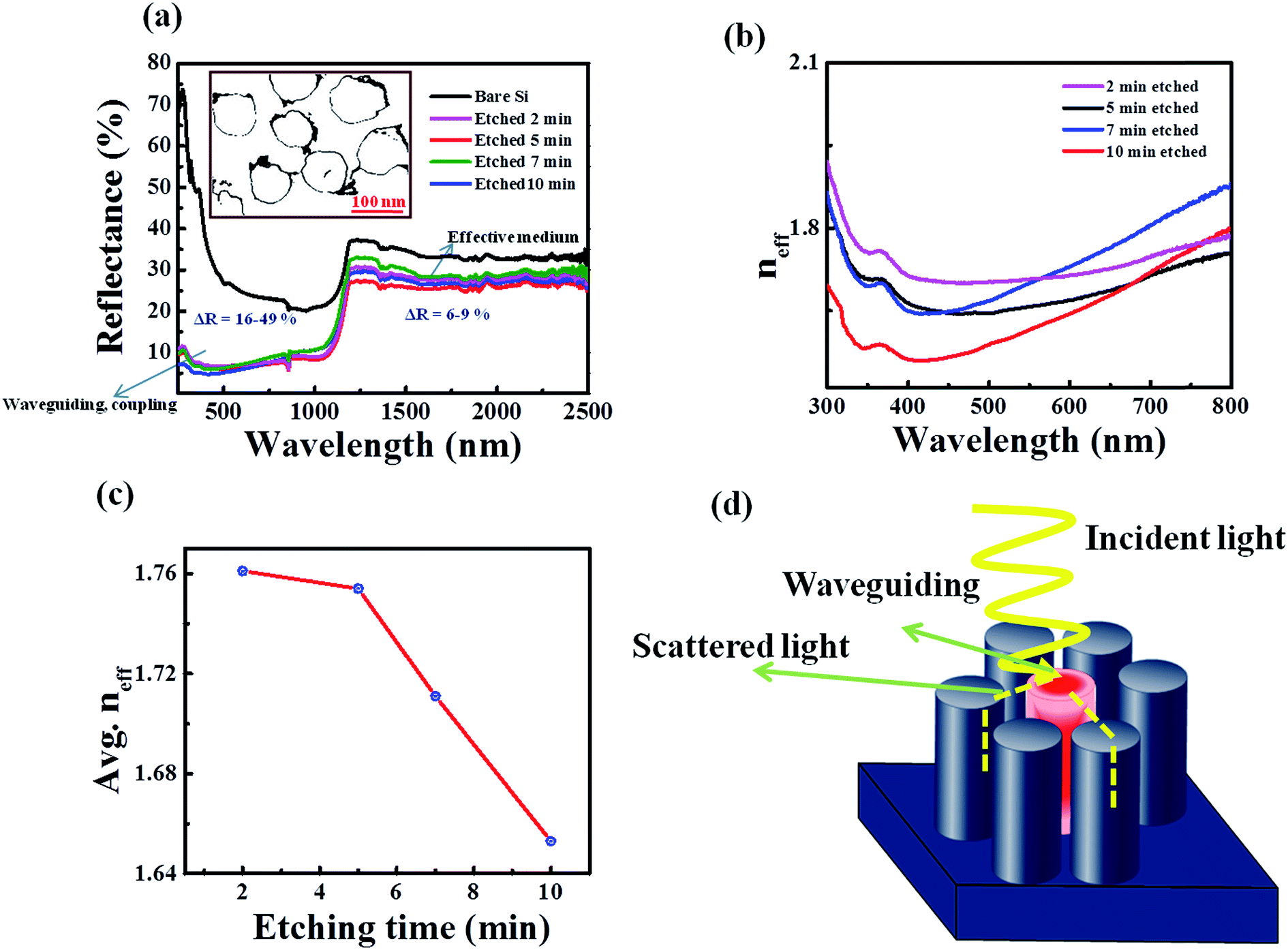 | ||
| Fig. 2 (a) Reflectance spectra of SiNPLs etched for different durations (b) effective refractive index neff of plot for SiNPLs etched for different time durations (c) variation of neff with etching time (d) schematic diagram shows the interaction of light with SiNPLs. | ||
The reflectance of our SiNPLs ranges from 21–23% by theory. The theoretical reflectance calculated by effective medium theory is very close to the experimental results at NIR region. In contrast, at the lower wavelength (300–800 nm) region the reflectance of the SiNPLs decreases remarkably in comparison to the bare Si. Reflectance of the SiNPLs reduced to 6.5, 4.6, 6 and 8% at wavelengths 300, 400, 600 and 800 nm respectively. The variation of refractive index (calculated from reflectance using Fresnel equation) in the wavelength region 300–800 nm and the average neff as a function of etching time are plotted in Fig. 2(b) and (c), respectively. A slight difference is observed in the behaviour of refractive indices of SiNPLs etched for 7 and 10 min. This must be due to the increase in inhomogeneous porosity on the top of the SiNPLs with etching, which is explained in the angle dependent Raman spectra. It can be seen from the Fig. 2(b) that the average effective refractive index (neff) of the SiNPLs decreases with the etching time. It is clear that the ultra low reflectance of SiNPLs in the visible region is not due to the effective medium theory since the variation neff in the visible region does not match with the theoretical value.
For the reflectance study, SiNPLs are illuminated parallel to the axis of the nanopillars as shown in Fig. 2(d). The wavevector of the incident light is perturbed by the high index nanopillars and gets coupled in to the leaky waveguide modes. The SiNPLs can act as a cylindrical dielectric waveguide for the propagation of light.32 The excitation of these waveguide modes causes absorption resonances. The generalized eigen value equation for the leaky waveguide mode is given by:25

Out of the various cylindrical dielectric waveguide modes our concern is with the lowest order modes such as TE01, TE11, TM01 and TM11 due to the symmetry matching requirements.33 The reflectance of the SiNPLs remains very low throughout the spectral range 300–800 nm.
In order to confirm the absorption resonance associated with the SiNPLs and to get a deeper insight to the light trapping property SiNPLs, we have performed FDTD simulation in bare and etched Si. The top view of the simulation region is shown in Fig. 3(a). The other details of simulation are given in ESI Fig. S2.† The FESEM top view of the SiNPLs is shown in the Fig. 3(c), the same structure we have modelled in FDTD simulation. The simulated results along with the experimental reflectance spectra are presented in Fig. 3(d). The wavelength less than 500 nm is absorbed by the SiNPLs and the wavelength greater than 500 nm is transmitted to the substrate. As a result, the effective reflectance stays quite low over the entire wavelength region. The absorption peaks located at 398 and 450 nm, which represent absorption resonances of the TM11 and TM01, respectively. The same absorption peaks are observed for the simulation using TE polarized source. To understand the origin of absorption resonance in SiNPLs, it is worth to describe the electric field distribution of SiNPLs at different wavelengths, as shown in Fig. 4. The absorption resonances associated with our SiNPLs are TM11, TM01, TE11 and TE12, respectively. The simulated results and electric field plot of bare Si are shown in Fig. S2.† The simulated total reflectance is in good agreement with experimental results at higher wavelength > 500 nm, whereas simulated reflectance exhibits substantial quantitative difference with the experimental reflectance at the lower wavelength region (<500 nm). This is attributed to the effective coupling due to the inhomogeneous porosity along the SiNPLs, which is not included in the simulation. The porous layer acts as a three dimensional grating to couple the light effectively in to the waveguide modes. This inhomogeneous porosity on the SiNPLs plays a major role in the omnidirectional light harvesting. The formation mechanism and the evolution of porosity on the SiNPLs are discussed in our previous paper.28 The porosity variation from the top to bottom of the SiNPLs and interaction with electromagnetic waves are explained in angle dependant reflectance and Raman spectra. A finite electric field (less than field inside the SiNPLs) can be seen between the SiNPLs at different wavelengths, which is attributed to the interpillar field coupling.26 The density of the SiNPLs is very high and the nanopillars are closely packed, so the modes associated with each nanopillar are perturbed by the presence of others. This perturbation causes the coupling and exchange of energy between the nanopillars. The essential physics behind coupling of nanopillars can be explained by Coupling Mode Theory (CMT). Cao et al. have demonstrated the CMT theory for silicon nanowires with experimental investigations.26 Moreover, the value of S0 in eqn (1) indicates the interpillar coupling; higher value of S0 even suppresses the reflectance. Notably, the suppression of reflectance in the SiNPLs is due to the combined effect of waveguiding and interpillar field coupling. Furthermore, the simulated reflectance results are in good agreement with the experimental data to a great extent and it supports the waveguiding property and CMT theory of SiNPLs.
 | ||
| Fig. 3 (a) Top view of the model used in FDTD simulation (b) the FESEM top view image of SiNPLs, which was used to model FDTD simulation (c) simulated results of the SiNPLs along with the experimental reflectance. | ||
 | ||
| Fig. 4 (a) E field distribution of TM modes in SiNPLs at different wavelengths (b) E field distribution of TE modes in SiNPLs at different wavelengths. | ||
To bring out the physics underlying the optics of the SiNPLs, we have performed the angle – resolved reflectance spectra of SiNPLs with TE (s) and TM (p) polarized light. The contour color plot for the angle – resolved reflectance spectra of SiNPLs with TM and TE sources for angle of incidence from 8° to 68° is shown in the Fig. 5(a) and (b), respectively. The ultra low reflection is observed for the TM polarization, since it has an electric field in the direction of the nanopillar axis, which enhances the absorption. In order to compare the dependence of polarization on the reflectance of SiNPLs, we have measured the reflectance of bare Si with TE and TM polarized light. The reflectance variation of bare Si with angle of incidence using TE and TM polarized light is shown in Fig. 5(c) and (d). The reflectance of bare Si varies from 30–70% for TE polarized light and 5–60% for TM polarized light with angle of incidence varying from 8–68°. On the other hand, the reflectance of SiNPLs stays less than 10% for TE polarized light with angle of incidence varying from 8–48°. The reflectance increases slightly on further increase in the angle of incidence, but which is still much less than bare Si. For TM polarized light the reflectance of SiNPLs is found to be less than 8% along the angle of incidence ranges from 8–68°. At 500 nm, the reflectance of TE and TM polarized light varies from 3–6% and 0.6–3% for the angle of incidence varying from 8–48°. Hence, it is clear that the reflectance of SiNPLs is insensitive to polarization with angle of incidence 8–48° in the visible region to a great extent.
 | ||
| Fig. 5 Angle-resolved reflectance spectra of SiNPLs with (a) TE polarized light (b) with TM polarized light (c) angle-resolved reflectance spectra of bare Si with TE polarized light (d) with TM polarized light. | ||
The angle resolved reflectance spectra of SiNPLs (etched for 2 min) as well as bare Si using unpolarized (normal) light is shown in Fig. 6(a) and (b). It can be seen from the contour plots that an ultra-low reflectance of <4% is observed for etched Si over a wide range of angle of incidence (8–48°) and for a broad range of wavelength (300–700 nm). Further, for an angle of incidence > 48° the reflectance increases slightly, but it remains less than 10%. At a particular wavelength, say 500 nm, the reflectance varies very slowly with angle of incidence (shown yellow line in Fig. 6(a)). At 500 nm, the variation in the reflectance is ΔRn = 0.56% for angle of incidence varying from 8–48°. On the other hand, the reflectance of plain Si is >60% at the lower wavelength region and >30% at the higher wavelength region for a broad range of angle of incidence, as shown in Fig. 6(b). The reflectance variation of bare Si at 500 nm is ΔRn = 5.76% for an angle of incidence 8–48° (yellow line in Fig. 6(b)). From these observations, it can be seen that the reflectance of the etched Si varies very slowly with angle of incidence in comparison with the plain Si. Thus, the angle dependent reflectance spectra literally show the omnidirectional light harvesting properties of the etched Si with respect to the plain Si. Moreover, the reflectance variation along the wavelength at a particular angle of incidence is also shown in Fig. 6(a) and (b) (red line). At a particular angle of incidence 38°, the reflectance variation of etched Si with respect to wavelength stays 0.09%, whereas for the plain Si the variation is found to be very large ∼23% in the visible region, i.e., the reflectance of the SiNPLs is independent of wavelength over a broad region. Thus, we can conclude that the broadband omnidirectional and wavelength independent superior light trapping property of the SiNPLs manifest potential applications in light harvesting devices.
 | ||
| Fig. 6 Contour color plots for the angle-resolved reflectance spectra of (a) bare Si (b) etched Si with normal light. | ||
The absorption spectra of SiNPLs with TE and TM polarized lights for angle of incidences varying from 8–68° are presented in Fig. 7(a) and (b), respectively. A shift in the broad absorption peak is observed for the SiNPLs, especially for the TM polarized light. To investigate the minor peak shift and the origin of the measured absorptance, the FDTD simulation was also performed with the same angle variation from 8–68° using TE and TM polarized light, as shown in Fig. 7(c) and (d), respectively. The simulated and experimental absorptance for TE polarized light decreases with increase in angle of incidence. For TM polarized light the absorption in both the spectra increases with angle of incidence till Brewster angle (60°) and then decreases. The mismatch between the experimental and simulated absorptance is observed in the lower wavelength region less than 450 nm, which is ascribed to the inhomogeneous porosity along the SiNPLs. Moreover, the minor shift in the absorption peak with angle variation is not observed in the simulated absorption spectra of SiNPLs. As we increase the angle of injection from 8–68°, the light has a propensity to focus towards the tip. In order to confirm the intuitive geometric contribution to the absorptance due to inhomogeneous porosity and waveguiding property, Raman spectra were recorded with different etching times and angle variation in back scattering geometry.
 | ||
| Fig. 7 Absorption of SiNPLs for an angle of incidence varying from 8–68° (a) experimental spectra with TE polarized light (b) simulated spectra with TE polarized light (c) experimental spectra with TM polarized light (d) simulated spectra with TM polarized light. | ||
Raman spectra of SiNPLs etched for 2, 5, 7 and 10 min in comparison with the bare Si are shown Fig. 8(a). The relative intensities of the etched Si with the bare Si clearly confirm the waveguiding property of the SiNPLs. The Raman spectrum of crystalline bulk silicon exhibits a symmetric Lorentzian profile centered at 521 cm−1 with FWHM of 6 cm−1 as shown in Fig. 8(b). In the case of bulk Si, the phonon momentum conservation, which implies K0 = KS ± KK, where KS and KK are the wavevector of scattered light and wavevector of lattice wave respectively, limits the Raman signal due to the optical phonons from the center of the Brillouine zone.34 The Raman peak of the etched Si is found to be red shifted to 519 cm−1 with FWHM 9 cm−1 and an additional lower energy tail at 512 cm−1. The origin of the lower energy tail is strongly believed to be due to the presence of porous structures in the SiNPLs. These porous structures consist of small crystallites of size less than 15 nm, which slack the phonon selection rules, cause more phonon modes to contribute for Raman scattering. These lower energy optical phonons induce broadening and redshift to the Raman spectrum. To fit the Raman spectrum of the porous SiNPLs, single Lorentzian fit may not give the accurate fitting since the SiNPLs comprised of both crystalline Si and porous Si. In order to fit Raman spectrum of etched Si accurately, it is required to use a fitting function which sums all the phonon modes that contribute to the Raman scattering.23 The Raman spectrum of SiNPLs fitted with Lorentzian and Voigt function is shown in Fig. 8(c). It can be seen that the Raman spectrum fitted with Lorentzian fails to capture the lower energy tail and the fit shows an R2 value of 0.94. The Voigt function which is a combination of both Lorentzian and Gaussian functions gives more accurate fitting with an R2 value of 0.99, shown in Fig. 8(c). This result shows that the SiNPLs consist of both crystalline Si (sharp peak) as well as porous Si (broader tail). The presence of porosity and the crystallites size are determined by BET sorption analysis, as shown in Fig. 9(a) and (b). BET adsorption and desorption isotherms of the porous SiNPLs performed at 77 K is shown inset of Fig. 9(a). The H3 type hysteresis loop clearly shows the capillary condensation in porous structures on SiNPLs.35 Non localized density functional theory (NLDFT) has been used for the pore distribution analysis. According to this method, the most of the pore size ranges from 4–16 nm and the most probable pore diameters are 4.5 nm and 8.8 nm, as shown in Fig. 9(a). The pore-volume histogram obtained from NLDFT analysis is shown in inset of Fig. 9(b). The DFT-Monte Carlo cumulative pore volume plot is also shown in the Fig. 9(b). The pore volume starts from a pore diameter of ∼2 nm and reaches maximum cumulative pore volume at ∼14 nm.
 | ||
| Fig. 8 (a) Raman spectra of SiNPLs etched for 2, 5, 7 and 10 min (b) Raman spectra of bare Si fitted with Lorentzian function (c) Raman spectra of etched Si fitted with Lorentzian and Voigt function. | ||
 | ||
| Fig. 9 (a) Differential pore volume–pore width plot and nitrogen adsorption–desorption isotherm of porous SiNPLs is shown in inset (b) NLDFT-Monte-Carlo cumulative pore volume plot for the porous SiNPLs. The histogram for the pore distribution of porous SiNPLs is shown in inset. (c) Schematic diagram for angle dependent Raman measurement (d) angle dependent Raman spectra of SiNPLs with angle of incidences 0, 15, 30 and 45°. | ||
The waveguiding property and the shift in the reflection minima of the angle resolved reflectance spectra can further be explicated using angle dependant Raman scattering. The schematic diagram for the angle dependent Raman measurement is shown in Fig. 9(c). The angle dependent Raman spectra of the SiNPLs for the angle of incidences 0, 15, 30 and 45° is shown in Fig. 9(d). As the angle of incidence increases from 0 to 45° the intensity of the Raman peak decreases. Since the Raman is recorded in back scattering geometry using TM polarized laser, the a fall in intensity with an increase in angle of incidence is observed, which we have already seen in the reflectance data with TM polarized light. The angle dependent Raman spectrum of the porous SiNPLs fitted with two peaks is shown in the Fig. 10. The narrow peak of crystalline Si and the broader peak of porous Si are found to be red shifted with increase in angle of incidence. The peak shift and the FWHM of the etched Si with angle of incidences are plotted in Fig. S3(a) and (b),† respectively. The enhancement in relative intensity and the integrated area of the low energy broad peak with angle of incidence to the entire fitted area in Fig. 10 clearly indicates the presence of additional phonon modes originate from the effective increase in porosity. From these results we conclude that, the increase in angle of incidence leads the light to interact with the region of high degree of porosity and at 45° the laser is focussed more at the tip, which bears highly porous structure. The variation of integrated area of the broader low energy tail APsi to the entire fit ASiNPLs and the intensity of the narrow peak with angle of incidence, is shown in inset of Fig. 10(c). As the degree of porosity increases towards the tip the crystallite size must be reduced due to the increase in void fraction.
 | ||
| Fig. 10 Raman spectra of SiNPLs fitted with two peaks for varying angle of incidences (a) 0° (b) 15° (c) 30° and (d) 45°. The peak shift observed plotted as a function of angle of incidence in angle dependent Raman scattering is shown in inset of (c) and intensity variation of the crystalline Si peak and ratio of integrated area of the broad porous peak to the crystalline Si peak is shown in inset of (c). | ||
The angle dependant Raman data and the BET measurements suggest that our SiNPLs possess a core/shell structure with solid core and porous Si shell. The thickness of the porous shell increases from bottom to top region of the SiNPLs. The porous shell layer induces the effective coupling and absorption of light, predominantly in the lower wavelength region. The increased porosity towards the tip of the SiNPLs leads to an effective decrease in the core radius of SiNPLs. The variation in the porosity and the core radius towards the tip observed in the angle dependant absorption spectra with a minor shift in the absorption peak is due to slight fluctuation in the absorption resonance of the SiNPLs. As a proof of concept, we have modeled a structure with step discontinuity to get a close resemblance to gradient refractive index condition. The simulated reflectance using this structure agrees with the experimental data over the entire wavelength, and the same is shown in Fig. S4.† Hence, we speculate the origin of the absorption peak shift and the reflectance mismatch at the lower wavelength region is due to the inhomogeneous porosity on the SiNPLs. The inhomogeneous porosity on the SiNPLs plays an incredible role in the omnidirectional and polarization insensitive light trapping.
Conclusion
In conclusion, the porosity variation on the top of the SiNPLs fabricated by metal assisted chemical etching, are characterized using angle dependent Raman scattering and BET measurements. These results suggest that the SiNPLs posses a core/shell structure with a solid Si core and porous Si layer and the thickness of the porous layer increases towards the tip. These mesoporous inhomogeneous porous structure plays a major role in the omnidirectional light trapping, especially in the lower wavelength region. The gradient refractive index produced by the mesoporous structure on the SiNPLs facilitates the coupling of light into the leaky waveguide modes. The waveguide modes associated with the SiNPLs are TE01, TE11, TM01 and TM11. An ultra low reflectance < 4% was observed over wide range of angle of incidence 8–48° in the visible region. FDTD simulation has been performed to determine the waveguide modes associated with the SiNPLs and to study the omnidirectional light trapping in SiNPLs theoretically. The studies on the omnidirectional light trapping are useful for the design of optoelectronic devices and this mesoporous SiNPLs also have applications in bio/chemical sensors and filters.Acknowledgements
The authors are thankful to the Director, CSIR-NAL for his support and encouragement. Mr G. Srinivas and Mr Siju John are thanked for various measurements. Dr Arvind kumar is thanked for various discussions. BRNS (Project No.: U-1-125) is thanked for SRF fellowship to K. P.References
- F. Priolo, T. Gregorkiewicz, M. Galli and T. F. Krauss, Nat. Nanotechnol., 2014, 9, 19 CrossRef CAS PubMed.
- L. Cao, J. S. White, J. S. Park, J. A. Schuller, B. M. Clemens and M. L. Brongersma, Nat. Mater., 2009, 8, 643 CrossRef CAS PubMed.
- C. Xie, B. Nie, L. Zeng, F. X. Liang, M. Z. Wang, L. Luo, M. Feng, Y. Yu, C. Y. Wu and S. H. Yu, ACS Nano, 2014, 8, 4015 CrossRef CAS PubMed.
- V. Krivitsky, L. C. Hsiung, A. Lichtenstein, B. Brudnik, R. Kantaev, R. Elnathan, A. Pevzner, A. Khatchtourints and F. Patolsky, Nano Lett., 2012, 12, 4748 CrossRef CAS PubMed.
- M. Kandziolka, J. Charlton, I. I. Kravchenko, J. A. Bradshaw, I. A. Merkulov, M. J. Sepaniak and N. V. Lavrik, Anal. Chem., 2013, 85, 9031 CrossRef CAS PubMed.
- A. K. Shalek, J. T. Robinson, E. S. Karp, J. S. Lee, D. R. Ahn, M. H. Yoon, A. Sutton, M. Jorgolli, R. S. Gertner, T. S. Gujral, G. MacBeath, E. G. Yang and H. Park, Proc. Natl. Acad. Sci. U. S. A., 2010, 107, 1870 CrossRef CAS PubMed.
- G. J. Zhang and Y. Ning, Anal. Chim. Acta, 2012, 749, 1 CrossRef CAS PubMed.
- Z. Huang, H. Fang and J. Zhu, Adv. Mater., 2007, 19, 744 CrossRef CAS.
- Z. Huang, N. Geyer, P. Werner, J. de Boor and U. Gosele, Adv. Mater., 2011, 23, 285 CrossRef CAS PubMed.
- L. Sun, Y. Fan, X. Wang, R. A. Susantyoko and Q. Zhang, Nanotechnology, 2014, 25, 255302 CrossRef PubMed.
- R. G. Hobbs, N. Petkov and J. D. Holmes, Chem. Mater., 2012, 24, 1975 CrossRef CAS.
- S. W. Chang, V. P. Chuang, S. T. Boles, C. A. Ross and C. V. Thompson, Adv. Funct. Mater., 2009, 19, 2495 CrossRef CAS.
- Y. K. Ryu, P. A. Postigo, F. Garcia and R. Garcia, Appl. Phys. Lett., 2014, 104, 223112 CrossRef.
- Y. Q. Fu, a. Colli, a. Fasoli, J. K. Luo, a. J. Flewitt, a. C. Ferrari and W. I. Milne, J. Vac. Sci. Technol., B: Microelectron. Nanometer Struct.--Process., Meas., Phenom., 2009, 27, 1520 CrossRef CAS.
- G. Barbillon, Updates Adv. Lithogr., 2013, 57, 197–208 Search PubMed.
- M. Sun, G. Kim, J. Han, H. Kim, S. Wan, H. Woo, J. Lee, H. Shin and B. Park, Microelectron. Eng., 2013, 110, 141 CrossRef CAS.
- B. R. Ji, W. Lee, R. Scholz, U. Gosele and K. Nielsch, Adv. Mater., 2006, 18, 2593 CrossRef.
- X. Li, Curr. Opin. Solid State Mater. Sci., 2012, 16, 71 CrossRef CAS.
- H. Han, Z. Huang and W. Lee, Nano Today, 2014, 9, 271 CrossRef CAS.
- A. Cowley, J. A Steele, D. Byrne, R. K. Vijayaraghavan and P. J. McNally, RSC Adv., 2016, 6, 30468 RSC.
- C. Chartier, S. Bastide and C. Levy-Clement, Electrochim. Acta, 2008, 53, 5509 CrossRef CAS.
- K. Q. Peng, X. Wang and S. T. Lee, Appl. Phys. Lett., 2009, 95, 243112 CrossRef.
- D. Ratchford, J. Yeom, J. P. Long and P. E. Pehrsson, Nanoscale, 2015, 7, 4124 RSC.
- Y. F. Huang, S. Chattopadhay, Y. J. Jen, C. Y. Peng, T. A. Liu, Y. K. Hsu, C. L. Pan, H. C. Lo, C. H. Hsu, Y. H. Chang, C. S. Lee, K. H. Chen and L. C. Chen, Nat. Nanotechnol., 2007, 2, 770 CrossRef CAS PubMed.
- K. T. Fountaine, W. S. Whitney and H. A. Atwater, Nanotechnology, 2014, 116, 153106 Search PubMed.
- L. Cao, P. Fan and M. L. Brongersma, Nano Lett., 2011, 11, 1463 CrossRef CAS PubMed.
- F. Teng, N. Li, L. Liu, D. Xu, D. Xiao and N. Lu, RSC Adv., 2016, 6, 15803 RSC.
- P. Karadan, S. John, A. A. Anappara, C. Narayana and H. C. Barshilia, Appl. Phys. A, 2016, 122, 669 CrossRef.
- S. Thiyagu, B. Parvathy Devi and Z. Pei, Nano Res., 2011, 4, 1136 CrossRef CAS.
- A. Kumar, S. Siddhanta and H. C. Barshilia, Sol. Energy Mater. Sol. Cells, 2016, 129, 147 CAS.
- J. Cai and L. Qi, Mater. Horiz., 2015, 2, 37–53 RSC.
- K. Seo, M. Wober, P. Steinvurzel, E. Schonbrun, Y. Dan, T. Ellenbogen and K. B. Crozier, Nano Lett., 2011, 11, 185 Search PubMed.
- M. L. Brongersma, Y. Cui and S. Fan, Nat. Mater., 2014, 13, 451 CrossRef CAS PubMed.
- I. Zardo, G. Abstriter and F. Morral, Raman Spectroscopy on Semiconductor Nanowires, 2010, ISBN 978-953-7619-79-4 Search PubMed.
- A. A. S. M. Radzi, S. F. M. Yusop, M. Rusop and S. Abdullah, Mater. Sci. Eng., R, 2012, 40, 012046 Search PubMed.
Footnote |
| † Electronic supplementary information (ESI) available. See DOI: 10.1039/c6ra20467h |
| This journal is © The Royal Society of Chemistry 2016 |