A method to derivatize surface silanol groups to Si-alkyl groups in carbon-doped silicon oxides

Srikar Rao Darmakkolla, Hoang Tran, Atul Gupta and Shankar B. Rananavare*
Department of Chemistry, Portland State University, Oregon 97201, USA. E-mail: ranavas@pdx.edu

Received 12th August 2016 , Accepted 19th September 2016

First published on 21st September 2016


Abstract

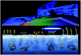
A carbon-doped silicon oxide (CDO) finds use as a material with a low dielectric constant (k) for copper interconnects in multilayered integrated circuits (ICs). Hydrophilic silanol groups (Si–OH) on its surface, however, can attract moisture, thereby causing an undesirable increase in the dielectric constant. Modification of the exposed hydrophilic surface to a hydrophobic functional group provides one solution to this problem. We report here a strategy for converting surface Si–OH to hydrophobic silicon hydride (Si–H) without affecting the internal oxide network in CDO. The approach involves esterification of the exposed silanol to its triflate (silyltrifluoromethanesulfonate, Si–O–Tf), followed by reduction to Si–H with diisobutylaluminum hydride. Si–H is further modified by a photochemical reaction with an alkene (1-octadecene) to yield Si–R (R = –C18H37) to provide a more moisture resistant, and less polar Si–C as opposed to the Si–O backbone. Fourier transform infrared (FT-IR) spectroscopy, X-ray photoelectron spectrometry (XPS), and measurements of the contact angle with water substantiated the successful conversion. The reaction scheme is versatile, transforming silanol groups to silicon hydride in widely varying chemical sites, from small molecules to the surfaces of silica gels, SiOx and CDO wafers. A comparison with the films (self-assembled monolayers) derivatized with the octadecyltrichlorosilane indicated that the new method leads to a thicker (≈5 nm) but more loosely packed hydrocarbon film with slightly lower contact angles.


1. Introduction

Advances in ultra-large scale integrated devices require replacement of traditional silicon oxide (SiOx), which has a dielectric constant (k) that is relatively high (k ≈ 4), with low-k materials for high-frequency operation (f ∼ 1/k). Contemporary low k materials provide an insulating sheathe, the so called inner layer dielectrics (ILD)s, between the copper metal interconnect lines in modern multilayered integrated circuits (ICs).1,2 Carbon-doped silicon oxide (CDO) is an important low k (≈2.5) material, crafted from organosilanes by plasma-enhanced chemical vapor deposition (PECVD).3–8 The resulting nanoporous CDO is composed of Si, C, O and H (SiCOH) with extensive cross-linking of Si–Si, Si–CH2–Si, Si–O–Si, Si–CH2–O–Si groups, creating a delicate porous network.9 The porosity/void fraction directly affects the dielectric constant and thermomechanical properties of the insulating CDO films.10 As the porosity (ϕ) increases from 0% to 50%, both k and thermal conductivity decrease continuously without significant discontinuity at the percolation threshold where the pores become interconnected. Similarly, thermomechanical properties such as thermal stress and its temperature-dependent slope decrease continuously with increasing porosity.

Fabrication of copper interconnects in modern ICs employs a well-known dual Damascene process to pattern CDO using optical lithography and copper deposition by electroplating,11 which are critical steps in the so-called back end of line processing (BEOL). Subsequently, oxygen plasma (ashing) removes the remaining sacrificial organic photoresist film deposited during lithographic patterning.12 An undesirable feature of O2 plasma is the generation of oxygen radicals which react not only with the photoresist film but also with the functional groups of the CDO film, breaking Si–CH3 and Si–H bonds, and creating dangling bonds of silicon. These dangling bonds can easily react with hydroxyl ions in the plasma environment to form Si–OH groups.13 The resulting increase in the number of hydrophilic Si–OH groups makes the CDO films more polar and hydrophilic and allows the uptake of moisture. Because kH2O = ∼80, absorbed moisture increases the value of kCDO. Current carried by protonic conduction14 leaks across the CDO, compromising its insulating quality leading to so “leaky” capacitors15 and contributes to high k values due to Maxwell–Wagner–Sillars polarization effects.16

Several approaches have explored the use of plasma processing to minimize the damage to films of porous CDO with ultra-low k. One method deposits a thin inert SiNx passivation layer to protect the CDO film from damage after the oxygen plasma. Ammonia (NH3) plasma exposure of a thin layer of hybrid-organic-siloxane-polymer (HOSP) produces the SiNx film.17 This inert layer can decrease the uptake of moisture by the HOSP film and increase its resistance to attack by O2 plasma. Another method entails treatment with helium (He) plasma after CDO deposition.18 Repair of the damage resulting from the O2 plasma by reducing silanol to silicon hydride has also been explored using hydrogen (H2) plasma.19 Overall the harsh reactive environment, during plasma processing, causes a thinning of the CDO films and irreversible modification of the Si–C–OH network.

An alternative to these plasma-based methods is a surface modifying chemical approach. For example, treatment with hexamethyldisilazane (HMDS) converts silicon-hydroxyl (Si–OH) functional groups on the damaged surface of the CDO to hydrophobic Si–O–Si(CH3)3.20 The resulting terminal methyl group, however, is insufficient to prevent further attack by moisture. Silanization with a longer alkyl is an obvious remedy, but it introduces undesirable polar Si–O functional groups that elevate k values of the film.

This report presents a gentle and spatially selective approach for modifying surface-exposed, hydrophilic silicon-hydroxyl (Si–OH) functional groups to hydrophobic hydrogen-terminated silicon (Si–H). The reaction scheme provided below further enhances the surface hydrophobicity by hydrosilylation of the Si–H with a long alkyl chain (Si–R, R = C18H37)21,22 and the resulting Si–C bond is far less polar and offers a lower k alternative.

Compared to methyl groups, the long chain alkyl groups form a thicker, close-packed hydrophobic film that effectively blocks the uptake of moisture.23 The significant advantage of this approach is that the selective derivatization occurs only on the exposed silicon-hydroxyl (Si–OH) groups of the CDO film without damaging the rest of the nano-porous cage. Also, the organic layer blocks the ionic migration through the exposed inner layer dielectric (ILD) surface. Furthermore, derivatization with different reactants with silicon hydride formed during the intermediate stage provides new surface functionalities.24 For example, it provides a convenient route for insertion of additional functional groups such as terminal amines in the alkene structure thereby enabling a rational way to interface with other semiconductors such as carbon nanotubes or members of III–VI systems.

The method extends easily to other applications. For instance, the hydrophilic surfaces of commonly used silica gel in chromatography or silica aerogels may be transformed to a hydrophobic surface. The aerogels exhibit exceptional properties such as low thermal conductivity, high porosity, high optical transmission, high specific surface area, low dielectric constant, low refractive index and low sound velocity. Its moisture sensitivity, however, limits its practical use.25,26 Various derivatization schemes use methyltrimethoxysilane (MTMS), hexamethyldisilazane (HMDS), dimethylchlorosilane (DMCS), trimethylethoxysilane (TMES), and hexadecyltrimethoxysilane (HDTMS) to alter the wetting properties of the surface.26 These methods replace hydrogen from the hydroxyl group (SiO–H)23,27–36 with a polar siloxy group (SiO–R) to render the surface hydrophobic. The method developed here instead replaces hydroxyl (–OH) groups with a nonpolar Si–C group bearing long alkyl chains (Si–R, R = CxH2x+1 or another hydrocarbon) which may be advantageous in certain types of chromatographic separations.

Following is a brief outline of the paper. We first present a synthetic approach to transforming small molecular silanol groups to silicon hydride to determine optimal reactions conditions for derivatization of solid surfaces of silica gel, SiOx and CDO coated wafers. We then combine our hydrogen termination method with the classic hydrosilylation route using octadecene to protect ILD better against the moisture infiltration. Next appears a comparison of our method with the classic silanization approach as revealed through electrical and optical properties of the corresponding films. The paper concludes with a brief discussion of the relevance of the chemistry for the BEOL processing.

2. Experimental section

2.1 Materials

tert-Butyldimethylsilanol ((CH3)3CSi(CH3)2OH), tert-butyldimethylsilyl trifluoromethanesulfonate (CF3SO3Si(CH3)2C(CH3)3), trimethylaluminum (Al(CH3)3), trifluoromethanesulfonicanhydride ((CF3SO2)2O, ≥99%), ethoxytriphenylsilanol (C20H20OSi), chloroform (CHCl3, ≥99%), anhydrous toluene (C6H5CH3, 99.8%) diisobutylaluminumhydride (((CH3)3CHCH2)2AlH), 1-octadecene (C18H36), and octadecyltrichlorosilane (C18H38SiCl3) were all reagent grade, purchased from Sigma-Aldrich and used as received. Sigma-Aldrich was the source of amorphous silica gel (high-purity grade (Davisil Grade 62), SiO2, 60–200 mesh, Chromatography grade). Intel Corporation provided CDO and SiOx coated silicon wafers.

2.2 Substrate preparation for heterogeneous chemical reactions

2.2.1 Silica gel. Above chromatography-grade silica gel, was reported by the manufacturer to have particle sizes ranging from 75 to 250 μm, 1.15 × 10⁻⁶ m3 g−1, and surface area of 300 m2 g−1, with a pore size of 15 nm. Before derivatization, the silica gel was dried by heating at 400 °C for 4 hours and allowed to cool under modest vacuum (100 mTorr).
2.2.2 SiOx and CDO wafers. 100 nm thick CVD deposited oxide wafers and CDO on silicon wafers, prepared using the plasma-enhanced chemical vapor deposition (PECVD) process, were a gift of Intel Corporation. Note that these oxide layers were deposited from vapor phase as opposed to thermally grown; the latter can have surface roughness below 0.1 nm when atomically smooth silicon wafers are used. Using standard RCA-1 cleaning solution (NH4OH, H2O2, H2O 1[thin space (1/6-em)]:[thin space (1/6-em)]1[thin space (1/6-em)]:[thin space (1/6-em)]5 v[thin space (1/6-em)]:[thin space (1/6-em)]v[thin space (1/6-em)]:[thin space (1/6-em)]v), CDO wafer coupons (1 × 2 cm in size) were cleaned and then dried under a stream of dry N2.37 Following the cleaning step, the wafers were washed several times in a dry N2 glove box with anhydrous toluene to remove any traces of adsorbed moisture before reaction.

2.3 Characterization

2.3.1 FT-IR spectroscopy. FT-IR spectra, collected in a transmission mode on a Thermoscientific, Nicolet™ iS ™5 FT-IR Spectrometer from 400 to 4000 cm−1 at a resolution of 4 cm−1, enabled qualitative estimation of functional groups. For collecting FT-IR spectra from samples of silica gel, small amounts of a sample (≈5 wt%) were mixed with KBr salt and pressed into thin pellets. CDO as well as SiOx wafers (1 × 2 cm) were placed directly in the path of the IR beam. After each stage of reactions, few samples were removed from a glove-box and their IR spectra collected in the ambient air (relative humidity 40–60%) which may account for partial hydrolysis or readsorption of ambient moisture that affected OH stretch vibration peaks in 3200–3600 cm−1. However, the samples, at the intermediate stages of derivatization, once removed from glove box were discarded after collecting their IR spectra. Thus, in all cases, the final IR spectra came from samples maintained in the glove box throughout all the stages of derivatization, i.e., these samples were never exposed to ordinary laboratory conditions till they had undergone all the steps in the derivatization scheme.
2.3.2 NMR spectroscopy. For NMR studies, reaction mixtures were dissolved in C6D6 or DMSO-d6 or CDCl3. Typical acquisition conditions for 1H- and 19F-NMR spectra, on a 400 MHz Bruker NMR instrument, used average of 256 scans. In all reactions discussed here, percentage yields were calculated from integrated peak intensities of 1H- or 19F-NMR spectra of crude mixtures.
2.3.3 Gas chromatography-mass spectrometry (GC-MS). GC-MS of test organic compounds and derivatives were collected in Agilent 7890 GC using 5975 Mass Selective Detector (MSD) operated in an electron-impact mode.
2.3.4 X-ray photoelectron spectroscopy (XPS). Derivatized and underivatized CDO and oxide wafer coupons (three samples each and three separate locations on a given coupon) were investigated using XPS. The instrument used was a PHI VersaProbe II Scanning XPS equipped with an argon (Ar)/C60 sputtering gun and dual-charge neutralizer. Data acquisition conditions for low-resolution survey spectra were: 187.85 eV pass energy, 1 eV per step, 20 ms per step, five cycles, and five sweeps. High-resolution spectra from Si (2p) region employed 23.5 eV pass energy, 0.1 eV step, 20 ms per step, five cycles, and five sweeps. Typical uncertainty in the estimated percentages for Si–X bond concentration varied between 3–5%.
2.3.5 Film thickness measurements. Filmetrics f20 spectrometer, operating in reflectance mode over the 400–1000 nm wavelength range, was employed for thin film characterization. Non-linear least squares fits of reflectance spectra, collected from silicon wafers bearing silicon oxide and CDO, gave the layer thickness and refractive indices as a function of wavelength. Squaring the measured refractive index yielded optical dielectric constants. Additionally, Gaertner Ellipsometer (He–Ne laser light source, λ = 632.8 nm, fixed incidence angle of 70°) supplanted the measurements of film thicknesses.
2.3.6 Contact angle measurements. A CCD camera (Kodak MDS 100) connected to a desktop computer acquired droplet images on the surface of CDO and SiOx wafers. The images were analyzed using the program ImageJ (Freeware available from NIH) to calculate the contact angle. Typical uncertainty in CA measurements was about 3–4°.

2.4 Common synthetic procedure for silica gel, SiOx and CDO wafers

The first step in reaction Scheme 1 employed 0.1 M triflic anhydride ((CF3SO2)2O) in anhydrous toluene at 50–60 °C for 48 hours to esterify the Si–OH functional group to yield silyltrifluoromethane sulfonate (Si–O–Tf, where Tf indicates the SO2CF3 group). In the second step, 0.1 M DIBAL-H (di-isobutylaluminum hydride, ((CH3)2CHCH2)2AlH) reagent at 50–60 °C for 48 hours reduced the triflate intermediate (Si–O–(SO2)CF3) to silicon hydride. Because hydrogen-terminated silicon is unstable, Si–H was further treated with 1-octadecene (CH3(CH2)15CH[double bond, length as m-dash]CH2) in the presence of UV light (254 nm) for 2 hours to produce Si–R (Si–C18H37).38 All reactions were carried out in dry N2 within a glovebox. Between each set of reactions, silica gel and CDO wafers were thoroughly washed with anhydrous toluene.
image file: c6ra20355h-s1.tif
Scheme 1 Developed chemical pathway to derivatize surface-exposed silanol to silicon hydride followed by alkyl termination.

2.5 Octadecyltrichlorosilane (OTS) derivatization of CDO and SiOx wafers

Nanoporous CDO and SiOx wafers (1 × 2 cm in size) were cleaned using RCA-1 solution and washed thoroughly with DI water. Then the wafers were cleaned with acetone, CHCl3, and anhydrous toluene solvents and followed by drying under the flow of dry N2 gas. As cleaned wafers were immersed in 50 mM solution of OTS in anhydrous toluene (99.99%) at room temperature and incubated for 24 hours. All the above steps were carried out in a dry nitrogen filled glovebox (moisture concentration < 50 ppm). After the reaction, OTS derivatized wafers were cleaned with anhydrous toluene, CHCl3, acetone solvents by ultra-sonication and followed drying under the flow of N2 gas.

2.6 Synthesis of tert-butyldimethylsilyltrifluoro-methane-sulfonate (TBDMS-OTf)

One mmol of tert-butyldimethylsilanol and two mmol of triflic anhydride was dissolved in 1 ml of anhydrous toluene and mixed at 50–60 °C for up to 72 hours. Percentage yields, calculated from the 1H-NMR of the crude reaction mixture (Fig. S1), were 30, 60, 98 and 100% for reactions lasting 2, 24, 48 and 72 hours, respectively.

1H-NMR (C6D6, 400 MHz) δ 0.60 (s, 9H) and δ −0.00 (s, 6H); 19F-NMR (CDCl3, 400 MHz) δ −76.84 (s, 3F); MS parent peak calculated for CF3SO3Si(CH3)2C(CH3)3 was 264.34 m/z, found at 265.0 m/z (Fig. S2); IR (KBr) νmax 3027, 2926, 2857, 1228, 1193, 1039 cm−1.

2.7 Synthesis of tert-butyldimethylsilane

One mmol of tert-butyldimethylsilyltrifluromethane sulfonate and two mmol of DIBAL-H reagents were dissolved in 1 ml of anhydrous toluene and mixed at 50–60 °C for up to 72 hours. Percentage yields, calculated from 1H- and 19F-NMR of the crude reaction mixture, were 0, 61, 89 and 91% for 2, 24, 48 and 72 hours, respectively (Fig. S3 and S4).

1H-NMR (CDCl3, 400 MHz) δ 3.64 (m, 1H), δ 0.88 (s, 9H), δ 0.02 (d, J = 3.1 Hz, 6H); MS parent peak calculated for H–Si(CH3)2C(CH3)3 was 116.28 m/z, found at 116.10 m/z (Fig. S5); IR (KBr) νmax 3027, 2926, 2857, 2105 cm−1.

2.8 Synthesis of tert-butyltrimethylsilane

One mmol of tert-butyldimethyltrifluoromethane sulfonate and two mmol of trimethylaluminum reagents were dissolved in anhydrous toluene and mixed at 25 °C for 24 hours.

1H-NMR (C6D6, 400 MHz) δ 0.93 (s, 9H), δ 0.01 (s, 9H) (Fig. S6); the MS parent peak calculated for (CH3)3SiC(CH3)3 was 130 m/z, found at 130.1 m/z (Fig. S7).

2.9 Synthesis of triphenylsilane

One mmol of ethoxytriphenylsilane and two mmol of DIBAL-H reagent were dissolved in anhydrous toluene and mixed at 50–60 °C for 48 hours. Percentage yield calculated from 1H-NMR of the crude reaction mixture was 48%.

1H-NMR (DMSO-d6, 400 MHz) δ 7.58 (m, 15H), δ 5.7 (s, 1H) (Fig. S8); IR (KBr) νmax 3067, 2119, 1427, 1113, 802, 730, 697 cm−1.

3. Results and discussion

Small organic molecules bearing silanol groups provided suitable model systems to optimize reactions conditions, such as temperature, duration and reactant concentrations, for reactions which are shown in Scheme 1. The optimized reaction conditions were applied to derivatize silica gel which presents a model solid surface bearing high concentration Si–OH groups. Simple transmissive IR spectroscopy allowed characterization of functional groups generated during derivatization reactions. Finally, the method was adopted to SiOx and CDO coated silicon wafers which have a relatively low concentration of surface accessible Si–OH groups. XPS, FT-IR and contact angle measurements indicated successful derivatization of these surfaces. Electrical and optical characterization of CDO and SiOx layers included measurements of low and high-frequency k values, and film thicknesses, respectively.

3.1 Reactions of model organic compounds

tert-Butyldimethylsilanol ((CH3)3CSi(CH3)2OH) served as a test molecule for the reaction scheme (Fig. 1a). Transformation of the molecule to triflate and hydride molecules can be readily tracked by NMR, IR and GC-MS (Fig. S1–S5), enabling optimization of the reaction conditions and yield. The kinetics of the triflation reaction was monitored by the 1H-NMR of the reaction mixture over 72 hours. The reaction reached completion (≈98%) within 48 hours based on proton NMR spectral analysis (Fig. S1).
image file: c6ra20355h-f1.tif
Fig. 1 Schemes for synthesis of: (a) TBDMS triflate and tert-butyldimethylsilane; (b) tert-butyltrimethylsilane; (c) triphenylsilane.

In the second step, the reduction of TBDMS-triflate to tert-butyldimethylsilane (Fig. 1a) was achieved by treatment with DIBAL-H. After 24 hours of reaction, the emergence of a new heptet caused by Si–H at δ 3.64 (m, 1H) suggested the formation of the hydrogen-terminated product (Fig. S3). The yield achieved at 48 hours was over 95%.

Treatment of the TBDMS-triflate with trimethylaluminum at 25 °C produced terminal methyl groups and synthesized t-butyl methyl silane (Fig. 1b, S6 and S7). Thus, DIBAL-H and trimethylaluminum reagents successfully reduced the triflate ester of a silanol to hydride and methyl groups, respectively. In addition to tert-butyldimethylsilanol, we have confirmed the hydrogen termination on ethoxytriphenylsilanol (Fig. 1c and S8).

3.2 Reaction on silica gel

Having established the feasibility of the Scheme 1, we explored its potential for derivatizing silica gel, which is structurally similar to CDO. Silica gel, with its a highly porous structure and a large number of air-exposed hydroxyl groups,39 provided a useful control heterogeneous substrate. The FT-IR allowed monitoring the progress of the reaction (Fig. 2). The IR spectrum (the black trace in Fig. 2) from the silica gel exhibited a broad peak at 3439 cm−1 caused by the superimposed stretching modes of Si–OH groups and the hydroxyl groups of physically adsorbed water. Peaks at 1626 cm−1, 1480 cm−1, were assigned to the bending vibrations of water and silanol, respectively. Peaks at 1102 cm−1 and 969 cm−1 reflected the Si–O–Si stretch vibration modes of the silica gel.23,27,29,31,32,34
image file: c6ra20355h-f2.tif
Fig. 2 FT-IR spectra of silica gel at various stages of the reaction: pure Si gel (black); after treatment with triflic anhydride (blue); DIBAL-H reduced (pink); and after treatment with 1-octadecene (red).

After reaction with triflic anhydride, FT-IR of silica gel (Fig. 2, the blue trace) exhibited new peaks at 1033 cm−1 and 1257 cm−1, corresponding to S[double bond, length as m-dash]O asymmetric and symmetric stretches, and an 1177 cm−1 peak ascribed to C–F stretching corresponding to the formation of triflate (Si–O–(SO2)CF3) groups. Because some OH groups on silica gel are inaccessible to triflic anhydride, the triflation reaction did not completely remove the broad OH peak. Other possibility includes readsorption of adventitious moisture from the air. Notably, the peak intensity increased after triflation perhaps due to incomplete removal of the triflic acid generated during the reaction, (1) the precise molecular mechanism for the observed enhancement in O–H peak intensities is unknown at this time.

Surface concentrations of silanol in a typical silica gel is 2.8 mmol g−1 with 4.6 SiOH per nm2.40 The percentage conversion of the surface silicon-hydroxyl to silyltrifluoromethanesulfonate ester was determined by 19F NMR spectroscopy of the reaction mixture based on the reaction between triflic anhydride and Si–OH on the surface of silica particles:

 
[triple bond, length as m-dash]Si–OH + (CF3SO2)2O → [triple bond, length as m-dash]Si–O–SO2–CF3 + CF3–SO2–OH (1)

19F NMR spectra exhibited chemical shifts of methyl fluorines in triflic anhydride (reactant) and triflic acid (product) remaining in the reacting solution at −72.6 ppm and −77.3 ppm, respectively (Fig. S10). The integrated peak intensities determined the extent of the triflation reaction, assuming that the only source of triflic acid was from the silanol esterification reaction (eqn (1)). Moisture, however, if present, can also hydrolyze the triflic anhydride to give two moles of triflic acid:

 
(CF3SO2)2O + H2O → 2CF3SO2–OH (2)

Therefore, a control experiment was carried out in the glovebox to assess the effect of adventitious moisture by stirring triflic anhydride solution in anhydrous toluene for 24 and 48 hours at 60 °C. The corresponding 19F NMR spectra of the reaction mixtures yielded (triflic acid)[thin space (1/6-em)]:[thin space (1/6-em)](triflic anhydride) ratios of 1[thin space (1/6-em)]:[thin space (1/6-em)]148 and 1[thin space (1/6-em)]:[thin space (1/6-em)]80 for the shorter and more prolonged stirring, respectively. With 0.2 g of silica gel, the corresponding ratios after 24 and 48 hours of triflation reaction at 60 °C increased to 1[thin space (1/6-em)]:[thin space (1/6-em)]9 and 1[thin space (1/6-em)]:[thin space (1/6-em)]2, respectively. These data indicated that the moisture present in the glovebox contributed negligibly to the triflic acid from reaction (eqn (2)). Based on these 19F-NMR data, the esterification reaction reached 44% completion after 24 hours, which subsequently increased to above 90% after 48 hours.

Reaction with the reducing reagent, DIBAL-H with silica gel yielded a new set of peaks in FT-IR at 2259 cm−1 and 888 cm−1, which correspond to Si–H stretching and bending vibrations, respectively27 (Fig. 2, the pink curve). The Si–H stretching frequency depends on the polarity of the other three bonds attached to the silicon, increasing from 2109 to 2250 cm−1 in going from C3Si–H to O3Si–H.41

Because of Si–O bond polarization, the attached Si–H bond tends to hydrolyze upon exposure to atmospheric moisture. A typical lifetime of the SiH group of the silica surface in the air as determined from IR studies was less than half an hour. We, therefore, used a well-known hydrocarbon-derivatization scheme for its protection.38 Silicon hydride groups (Si–H) were hydrosilylated (Si–R) by treating the powder with 1-octadecene in the presence of UV light (254 nm) for 2 hours. Samples were washed with anhydrous chloroform (CHCl3) to remove excess adsorbed 1-octadecene and then air dried.38,42 New IR peaks (Fig. 2, the red curve) at 2856 cm−1 and 2927 cm−1, corresponding to –CH2 symmetric and antisymmetric stretches, and a shoulder peak at 2974 cm−1 corresponding to –CH3 confirmed the alkyl-chain derivatization of the silica gel surface.23,29,31,32,34,35 Previous studies of the effect of surface curvature on the formation of SAMs indicated that higher curvature led to less ordered liquid like monolayers.43 It was noted that SAM of a C12-silanes on 9 nm radius of curvature silica particles caused to a shift of FT-IR peak due C–H antisymmetric stretch from 2925 cm−1 for a planar surface to 2929 cm−1 for the 9 nm curved surface. In light of 15 nm pore size of the silica particles used in our study, the observed shift is consistent with these previous finding. The same study established that a decreased packing density (i.e. decreased extent of derivatization) could also blue-shift the IR peak in the direction observed. An elegant approach to quantify the extent of silicon derivatization using solid-state NMR CP-MAS (Cross-Polarization and Magic Angle Spinning) technique was established which exploited quantitative analysis of the peaks corresponding to derivatized and underivatized Si atoms.44

In the FT-IR spectrum of alkyl-derivatized silica gel, the disappearance of peaks corresponding to alkene C–H stretch (C[double bond, length as m-dash]C–H) at 3083 cm−1 and the C[double bond, length as m-dash]C stretch at 1644 cm−1 indicated the absence of 1-octadecene physically adsorbed to the surface of the silica gel. To gauge further the effect of adsorbed alkenes, as opposed to chemically bonded alkyl groups, we conducted another control experiment. The dried silica gel was immersed in 1-octadecene, and exposed to UV light under identical conditions. The FT-IR spectrum (Fig. S11) of silica gel after these steps showed no significant peaks corresponding to alkyl chains, indicating negligible adsorption of 1-octadecene on the silica surface.

3.3 Reactions on SiOx wafer

Derivatization studies of SiOx coated wafer provided a suitable comparison with silica gel (vide supra) and low k dielectric, CDO (vide infra). These studies utilized silicon wafers decorated with 100 nm thick silicon oxide treated identical reaction conditions. The surface of the CVD oxide had an average roughness of 0.41 nm as determined by AFM (see Table S1 in ESI). A clean SiOx wafer before the reaction showed the peaks (the black trace in Fig. 3) corresponding to the stretching (3376 cm−1) and bending vibrations (890 cm−1) of the silanol (Si–OH); the symmetric (890 cm−1) and antisymmetric stretching (1105 cm−1) of cage Si–O–Si; and the bending vibration (610 cm−1) of Si–O–Si.9 Lower peak intensities associated with O–H stretch vibrations (at 3500 cm−1) when compared to Si–O–Si peaks (at 1100 cm−1), indicated a lower net content of surface Si–OH groups on SiOx wafer films than silica gel (cf. black curves in Fig. 2 and 3).
image file: c6ra20355h-f3.tif
Fig. 3 FT-IR spectra of SiOx wafer at various stages of the reaction: clean SiOx film (black); after treatment with triflic anhydride (blue); DIBAL-H reduced (pink); and after treatment with 1-octadecene (red).

The Si–OH absorption peak intensity significantly reduced upon triflation consistent with the surface accessibility of most Si–OH groups in the SiOx film (cf. black and blue traces). After the triflation reaction, new peaks appeared at 1039, 1228 cm−1 and 1193 cm−1 corresponding to symmetric and antisymmetric stretches of S[double bond, length as m-dash]O bond, and C–F stretch, respectively, as in the case of silica gel. However, their relative peak intensities were proportionately smaller. After DIBAL-H reduction the Si–H peak at 2259 cm−1 was not observed presumably because of the lower total content of SiOH groups on the SiOx film surface compared to silica gel (cf. pink curves in Fig. 2 and 3; also see below). Nevertheless, silica gel Si–H peaks disappeared upon exposure to air within half an hour. Similar limited stability of the Si–H groups in the air has been previously noted45 when the remaining three group bound to silicon are highly polar, such as Si–O.

We proceeded with hydrosilylation of the hydrogen-terminated surface with long-chain terminal alkene without exposing the sample to atmospheric moisture. Upon derivatization, we observed a decreased surface roughness (0.34 nm vs. 0.41 nm, Table S1) along with hints of island type structures (Fig. S18a).

After the photochemical reaction, the presence of peaks at 2853 and 2924 cm−1, corresponding to CH2 symmetric and antisymmetric stretches, and a shoulder peak at 2976 cm−1 (red curve and red inset in Fig. 3) confirmed the hydrosilylation. Compared to silica gel (2927 cm−1), the lower value of C–H asymmetric stretch vibration is consistent with a more ordered hydrocarbon layer on a smoother surface as discussed before. Nevertheless, the chains are not packed in crystalline state43,46 which would have resulted in the blue shift of the peak position to 2917 cm−1. The ratio of C–H (2800–2950 cm−1) to Si–O–Si (1100 cm−1) peak intensities was higher than silica gel (cf. Fig. 2 and 3) and could arise from a greater percentage of inaccessible surface SiOH groups in silica gel. The absence of peaks at 3083 and 1004 cm−1 corresponding to alkene C[double bond, length as m-dash]C–H stretching and bending vibrations, and the C[double bond, length as m-dash]C stretch at 1644 cm−1 of 1-octadecene, suggested that 1-octadecene was chemically bonded to the silicon surface rather than physically adsorbed. Contact angles before and after derivatization of SiOx surfaces were 10° and 91° respectively.

3.4 Reaction on CDO (carbon doped oxide) wafer

FT-IR, X-ray photoelectron spectroscopy (XPS) and water contact angles (CA) techniques were employed to monitor the progress of the reaction, and the appearance of new functional groups on CDO wafer surfaces. When compared to SiOx wafer the water contact angle on CDO after RCA clean, was significantly higher (35° vs. 10°, see Table 1, below) consistent with a more hydrophobic surface due to its higher carbon content and a lower density of SiOH group (cf. black curves in Fig. 3 and 4).
Table 1 Contact angle, film thicknesses of CDO and SiOx wafers
Sample Refractive index (η) kopt = η2 Overlayer thickness (nm) Overlayer thickness (nm) Hydrocarbon layer thickness (nm) CA (deg.)
Filmetrics Ellipsometry Filmetrics Ellipsometry
CDO clean 1.457 2.12 101.2 ± 0.6 102.9 ± 0.6 0 0 36 ± 3°
1-Octadecene deriv. CDO through DIBAL-H 1.447 2.09 103.1 ± 2.4 123 ± 4 2 ± 3 10 ± 5 87 ± 3°
OTS deriv. CDO 1.412 1.99 106.4 ± 0.3 107.2 ± 0.9 5 ± 1 4 ± 2 91 ± 4°
SiOx clean 1.473 2.17 107 ± 2 115.1 ± 0.3 0 0 11 ± 2°
1-Octadecene deriv. SiOx through DIBAL-H 1.448 2.09 111.2 ± 0.9 117.0 ± 2.4 4 ± 3 2 ± 3 101 ± 4°
OTS deriv. SiOx 1.435 2.06 118.9 ± 0.6 117.0 ± 0.9 2 ± 3 2 ± 1 105 ± 3°


image file: c6ra20355h-f4.tif
Fig. 4 FT-IR spectra of CDO wafer in various stages of reaction; clean CDO (black), after reaction with triflic anhydride (blue), after reaction with DIBAL-H (pink), after glacial acetic acid washing (green) and after octadecene derivatization (red). Stars indicated in the DIBAL-H treated spectrum correspond to alkyl groups arising from the surface bound, excess DIBAL-H reaction products. Insets expand selected spectral regions of triflic anhydride Tf2O and octadecene-derivatized silica in the IR spectra.

Morphological AFM studies, (Fig. S17 and Table S1) revealed the nanoporous nature of CDO. An average roughness of 0.37 nm was comparable to the CVD SiOx surface discussed earlier. Line scans revealed valleys as deep as 2 nm and the lateral features of 20 nm or smaller size broadened by AFM tip effects.47 Thus studies presented in this paper differ from atomically smooth silicon or silicon oxide surfaces.48

Fig. 4 shows the transmission FT-IR spectra of a CDO wafer at different stages of derivatization. Major peaks observed correlated well with the SiOx wafer IR peaks illustrated in Fig. 3. However, significantly lower peak intensity in the OH vibrational frequency range (≈3300 cm−1) compared to silica gel or SiOx wafer (Fig. 2 and 3), implied a lower net content of OH on the CDO surface. Accordingly, after triflation, intensities of peaks associated with S[double bond, length as m-dash]O and C–F stretches, (shown Fig. 4, the blue curve (inset)), were smaller than the corresponding peaks observed in the triflated SiOx films (blue curve, Fig. 3).

Reduction of triflate ester on the CDO surface using DIBAL-H proceeded as in the case of SiOx.49 After reduction with DIBAL-H several new peaks, not observed in silica gel or SiOx surfaces, appeared in the range from 2800–3000 cm−1, attributed to alkyl C–H vibrations. These peaks could originate from traces of the degraded DIBAL-H reagent (e.g. diisobutyl groups), physically adsorbed or trapped in pores of CDO surface (pink trace, Fig. 4). Also, supporting the above hypothesis was an observed increase in the peak intensity near the OH region (3300 cm−1) due to the formation of Al–OH group a byproduct of the reduction reaction. Since an aluminum oxide or its hydroxide dissolves readily in an acidic medium, we treated the wafer with 25% glacial acetic acid in anhydrous toluene for five minutes to remove trapped/degraded DIBAL-H reagent from the CDO surface. The FT-IR spectra collected after the acid treatment displayed a reduction in OH peak intensity and disappearance of alkyl shoulder-peaks (the green trace, Fig. 4).

A control experiment to further test the hypothesis of DIBAL-H binding on the CDO surface, entailed treating clean CDO, SiOx wafers, and silica gel sample with a DIBAL-H reagent (see Fig. S12) in anhydrous toluene. After 24 hours, samples were washed with dry toluene and dried. Their FT-IR spectra revealed the alkyl peaks only for the CDO confirming preferential DIBAL-H trapping/adsorption on the surface/pores of a slightly hydrophobic CDO surface (vide supra) as opposed to hydrophilic surfaces of silica gel or SiOx wafer.

Like SiOx wafer, Si–H stretching peaks were not detected presumably either because of low surface concentration or rapid degradation in the air42 during FT-IR data acquisition. Furthermore, observed weaker IR peak intensities (blue inset in Fig. 4) for the triflate groups on CDO and SiOx wafer surface compared to silica gel (blue curves in Fig. 2, 3 and 4) supported the above interpretation. FT-IR spectrum after hydrosilylation was similar to SiOx wafer results (cf. red curves in Fig. 3 and 4). A control experiment involving hydrosilylation of underivatized CDO surface revealed a lack adsorption of octadecene or its photochemical reaction product (Fig. S13). The observation of DIBAL-H adsorption/trapping (Fig. S12) but not of octadecene on clean CDO surface (Fig. S13) implied that a slightly hydrophilic CDO pores were unable to retain nonpolar octadecene, pointing to the amphipathic nature of the pore wall. This weaker pore-octadecene interaction would result in immediate removal of octadecene, but not DIBAL-H, during the CDO wafer rinsing/drying stage, before collecting respective IR spectra. In theory, following DIBAL-H reduction of pore surface triflate groups, octadecene could enter CDO pores and derivatize the hydrophobic silicon hydride pore surfaces (red curve Fig. 4). Alternatively, the steric effects such as nanopore size could preclude entry of larger octadecene while allowing smaller DIBAL-H molecule. Future studies using smaller size alkenes are planned, however, with the data at hand, we are unable to verify whether the internal pore surface is derivatized or not.

Antisymmetric stretching vibration due to C–H group occurred, as in the case of SiOx wafer, at 2924 cm−1. Also, within a factor of two, the C–H vibrational peak intensities were also comparable to those observed in derivatized SiOx wafer. These findings suggested that the hydrocarbon layers in both CDO and SiOx wafer surfaces were fluid and ordered analogous to lipid-chain packing in a lamellar liquid crystals.50–53 AFM studies revealed that the surface roughness on CDO surface upon octadecene derivatization decreased from 0.37 nm to 0.22 nm (Table S1) indicating the formation of a smooth hydrocarbon layer and possibly multilayer islands (Fig. S18b and Table S1). Thus, the growth of these hydrocarbon layers was rather complex somewhat analogous to Stranski–Krastanov model.54

A complementary technique of X-ray photoelectron spectroscopy (XPS) further supported for derivatization on CDO wafers. Survey spectra obtained from a CDO surface before (Fig. 5a) and after (Fig. 5c) reaction revealed Si, C, and O elements. After derivatization, the intensity of the carbon (1s) peak increased, consistent with the derivatization of surface groups with alkyl chains. In deconvoluted high-resolution Si (2p) spectra of clean CDO wafers before the reaction (Fig. 5b), three strong peaks at 101.6, 102.3 and 103.1 eV corresponding to Si–C, –Si–O–C– and –O–Si–O–, respectively were observed. The XPS spectrum after the reaction (Fig. 5d) had the same three strong peaks at similar positions but with different intensities. The area of the –O–Si–O– peak decreased from 26% to 10% of the Si (2p) peak area, and the relative area of –Si–C peak increased from 11% to 22%.


image file: c6ra20355h-f5.tif
Fig. 5 XPS spectra of CDO wafer. Survey spectrum, (a), and Si (2p) high-resolution spectrum, (b), collected before the reaction and (c) and (d) are the corresponding spectra collected after the reaction.

This finding validates conversion of –O–Si–OH to –O–Si–R (R = octadecyl). No significant change was observed in the areas for the –Si–O–C– group (from 57% before derivatization to 54% after derivatization), suggesting that no structural modification in the cage structure of the CDO film took place. More surface chemical studies are needed to confirm this hypothesis.

Derivatization of the CDO surface with octadecene should change its hydrophobicity. The contact angle of water droplets deposited on the surface confirmed that shift (Fig. 6). Clean CDO wafers (Fig. 6a) had a low contact angle 36° caused by the presence of the hydrophilic hydroxyl groups (Si–OH). Derivatization with octadecene increased the contact angle to about 90° (Fig. 6b and Table 1). The water contact angles on derivatized surfaces were stable for more than a year (see Fig. S14) as were the corresponding IR spectra (Fig. S15).


image file: c6ra20355h-f6.tif
Fig. 6 Water contact angles measured on (a) un-derivatized and (b) octadecene derivatized CDO wafers.

3.5 Comparison with octadecyl trichlorosilane (OTS) derivatization

OTS, a commonly used silanization agent, readily forms a self-assembled monolayer on SiOx film transforming it to from hydrophilic to a hydrophobic surface by inserting an alkoxy ether (Si–O–R) group bearing a C18 alkyl chain. Hence, we compared the results of octadecene-based vs. the OTS-based derivatization on CDO and SiOx surfaces. FT-IR spectra shown in Fig. 7 (for full spectra, see Fig. S16), indicated that the antisymmetric stretch was essentially constant at 2924 cm−1 regardless of the substrate or the derivatization method used. Both the oxide and CDO surface are nanoporous, which could prevent the formation of planar crystalline monolayers. This invariance of the peak position rules out any significant difference in hydrocarbon ordering between derivatization modes, i.e., OTS vs. octadecene. Nevertheless, it is hard to quantitatively disentangle the competing effects of curvature and packing density as discussed before. Curiously, the intensity of the IR peaks was consistently higher for octadecene derivatization than the OTS SAMs (blue vs. red traces). One potential explanation for this could be due to formation of multilayers46,55 (vide infra). AFM studies (Table S1) revealed a reduction in surface roughness upon derivatization and multilayer island formation in the case of CDO surface.
image file: c6ra20355h-f7.tif
Fig. 7 Comparison CDO and SiOx wafer derivatized by DIBAL-H assisted chemistry (blue) vs. OTS chemistry (red). Black curves depict IR spectra of the respective wafers before derivatization.

The silanol peak intensities, around 3300 cm−1, were greater in the OTS derivatized surfaces. An increase in OH peak intensity could come from the free Si–OH groups on the hydrolyzed OTS molecule as schematically illustrated in Fig. 7 (inset). These free O–H groups could provide interfacial hydrophilic sites for water adsorption underneath the alkyl chains of the OTS film. Thus, an insertion of Si–OR group which has a higher dipole moment than Si–R group and new free –OH groups would be expected to increase the k values of CDO/oxide films derivatized using OTS.

3.6 Effects of derivatization on dielectric constant and contact angle

Effects of Maxwell–Wagner polarization (MWP) hampered the low frequency (0.1–1 MHz) electrical measurements of k values due to adsorption of moisture in nanopores of CDO. Partial dissociation of trapped/adsorbed water molecules imparts the film a finite electrical conductivity creating electrically leaky (resistive) as opposed to insulating films.14 Such samples56 have higher dielectric contribution arising from distortion and dipolar polarization which raises their effective k.57 To disentangle MWP and other polarization effects require measurements of the film porosity, frequency dependent dielectric constants as a function of water saturation58 (i.e., humidity). Since these data were unavailable, we provide a qualitative description of our k (1 MHz) measurements (Fig. S19) that revealed following ordering in the magnitude of kOTS > kCDO > kDIBAL-H, consistent with the expected interfacial polarity of these samples (vide supra). One way around this problem is to reduce surface SiOH group concentration by high-temperature baking in an inert environment, and such studies are currently underway (vide infra).

Another approach to access k is through measurements of film refractive index; noting that high frequency (optical) k values simply depend on the electronic polarization and scale as the square of refractive index.59 Note, k values at optical frequencies do not contain dielectric contributions from MWP and dipole polarizations57 (see below). Analysis of reflectance spectra (Filmetrics) collected from these wafers yielded best-fit values of refractive index and film thickness; tabulated in Table 1. Best-fit refractive index values for CDO films were lower than SiOx film commensurate with the porous structure of CDO that can trap either water or air, both of which have lower refractive indices than SiO2. Furthermore, the effective refractive index values of OTS derivatized films were consistently lower than the octadecene derivatized implying perhaps their larger adsorbed moisture content. In either SiOx or CDO films the refractive index of DIBAL-H-treated films was greater than the OTS-treated films corresponding to its thicker hydrocarbon film of the greater refractive index (1.4439) than refractive indices of either water (1.33) or air (1.0).

To estimate film porosity of CDO crudely, the refractive index of these composite films (ηexp) was decomposed as a sum of volume fraction (φ) weighted refractive indices of the constituents:60

 
image file: c6ra20355h-t1.tif(3)
where index i denotes a specific component and φi its volume fraction. Assuming that the CDO matrix is made up of SiO2 (ηSiO2 = 1.473) and pores are filled completely with either air (ηSiO2 = 1) or water (ηH2O = 1.333) gave approximate the effective porosity of 3 or 11 percent respectively. Within limits of optical measurements of the film thickness using filmetrics, the hydrocarbon layer thickness in octadecene derivatization scheme were comparable (≈5 nm) for both CDO and SiOx (Table 1). These values were significantly higher than expected for a densely packed upright monolayer of C18 chain (2 nm). Ellipsometric measurements (Table 1) also gave a higher thickness of hydrocarbon layer in octadecene derivatized samples. The estimated hydrocarbon thicknesses were much smaller than the wavelength of light, suffered from higher uncertainties since they represented a difference of thickness before and after derivatization. Further the formation of island structures as indicated in the AFM studies (Fig. S18) contributed to the increased uncertainty. AFM studies presented in Table S1 also indicated island thickness of 4–6 nm, corresponding to bi–tri layer formation. Overall, these three independent techniques (AFM, refractive index and ellipsometry) qualitatively suggested the formation of multilayers upon octadecene derivatization which was further supported by higher IR peak intensities for the C–H stretch vibrations (Fig. 7) when compared to OTS derivatized monolayer films. The origin of multilayer formation could be justified by partial cross-linking/polymerization of octadecene during the hydrosilylation step.55

The contact angle measurements revealed similar trends. The contact angles for both derivatization schemes depended on the chemical nature of oxide layer, i.e., CDO vs. SiOx and not on the chemical route of derivatization, i.e., silanization vs. hydrosilylation. The CDO surface, which had a higher contact angle before derivatization (36° (CDO) vs. 11° (SiOx)), exhibited a lower contact angle after derivatizations (87° (octadecene) vs. 91° (OTS)) compared to the CVD SiOx surface (101° (octadecene) vs. 104° (OTS)). For CVD SiOx surface the observed contact angles after derivation were indicative of a more loosely packed fluid monolayer compared to the almost crystalline OTS monolayers assembled on SiOx grown thermally on smooth silicon surface61 that are known to exhibit 112° water contact angle.

Although the use of Cassie–Baxter equation has been controversial, we justify its use following Marmur et al.62 who summarized “The condition under which the Wenzel or Cassie equation correctly estimates the most stable contact angle is reiterated and demonstrated: these equations do hold when the drop size is sufficiently large compared with the wavelength of roughness or chemical heterogeneity”. Note, in present study, surfaces of CDO/SiOx exhibited nanoscopic topological features (Table S1) and the contact angle measurements employed macroscopic droplets. Thus, applying the Cassie equation for a measured contact angle (θm) on a surface made up of two types of regions (labeled with superscripts 1 and 2) with differing contact angles, θ1 and θ2, gives:63,64

 
cos[thin space (1/6-em)]θm = f(cos[thin space (1/6-em)]θ1 − cos[thin space (1/6-em)]θ2) + cos[thin space (1/6-em)]θ2 (4)
where f represents a fraction of the surface of type 1. Crudely, identifying region 1 as SiOx (θ1 = 11°) and region 2 as pores (i.e., air with θ2 = 180°) on CDO surface, the estimated upper limit for f = 0.91 implying a 9 percent surface porosity. Should the lower OH density on the CDO surface is accounted for by setting (θ1 > 11°) the measured porosity would decrease. For example, if θ1 = 30° for the nonporous CDO surface, then the calculated pore fraction would be 3 percent, similar to the estimates from the refractive index measurements (vide supra). Since we did not have a nonporous CDO sample, we did not have a value for θ1. Given these low areal fractions of pores and sub-nanometer roughnesses for the CDO and CVD oxide surfaces, these oxide films were treated essentially as smooth surfaces. So the Cassie equation could be inverted to extract the extent of surface derivatization/packing density of chains at the interface.

Now ascribing region 1 to the hydrocarbon monolayer (θ1 = 107°) and region 2 to the underivatized SiOx (θ2 = 11°, from Table 1), estimated f values were 0.97 for OTS and 0.92 for octadecene derivatized SiOx surfaces. By contrast, the CDO surface (θ1 = 87 and 92° and θ2 = 37°) had a thicker and perhaps even more loosely packed hydrocarbon layer due to the lower density of surface OH groups. The corresponding f values on the CDO surfaces were, as expected, were smaller; 0.75 (OTS) 0.69 (octadecene) respectively. The results also illustrated that the hydrocarbon layer thickness, which tended to be higher for the octadecene derivatization (Table 1 and Fig. 7), did not affect the contact angle, but the areal fraction of derivatized (i.e., f) surface did. One significant limitation of above analysis of the extent of derivatization is that it approximates θ2, contact angles for the clean surface, to be equal to the contact angle of smooth, nonporous CDO and SiOx surfaces because we did not have access to equivalent smooth surfaces.65

The reaction of hydrofluoric acid (HF) can also enhance the hydrophobicity of the silicon surface by creating a hydrogen-terminated surface that may be hydrosilylated, but it would produce undesirable etching of the CDO film. Recently, we have used sacrificial silanes to prevent the etching of SiOx by HF. The chemistry, however, is carried out in an aqueous medium of low pH, which would likely reoxidize Si–H groups66 and hence undesirable for this protecting the inner layer dielectrics from moisture.

3.7 General discussion

In modern interconnect fabrication, low k materials have become increasingly important, and several reviews emphasizing processing and chemical aspects have appeared in literature.67 Besides low k, the key requirements of these ILD insulators are film hardness, processability at temperatures as high as 400 °C, and low coefficient of thermal expansion. The success of CDO based dielectrics over the last two decades stems from their ability to meet these challenging demands. However, the path forward is now more demanding as simply increasing the porosity of films to reduce k further is not practical as it leads to undesirable features such as unacceptable line roughness, lower hardness and film cracking. The latter feature is especially problematic for chemical mechanical polishing (CMP) steps used in the BEOL processing. The introduction of carbon in SiOx backbone gives film toughness but at the cost of lower hardness. Thus, inserting hydrocarbons at the porous surface seem to be one avenue for optimizing low k materials in terms pore sealing, preserving hydrophobicity and reducing interfacial dipoles. At current GHz clock speeds, primary contribution to dielectric constant comes from dipolar, electronic and distortion polarizations as predicted from the classic Debye equation:
 
image file: c6ra20355h-t2.tif(5)
where αe and αDistort are electronic (the only contribution at optical frequencies) and distortion polarizations respectively; μ is the dipole moment, and N is its number density. Clearly, the dipole moment contribution is quite significant since it affects k quadratically. The dipole moments for Si–O68 and Si–C69 bonds are 3.08 D and 0.6 D respectively, so to lower k, it is advantageous to insert more Si–C bonds. However, bond enthalpy of Si–O bond is 450 kJ mol−1 vs. 290 kJ mol−1 for Si–C bond making films containing Si–O bonds harder than Si–C bonds. Nevertheless, these considerations are not relevant for the dangling Si–OH groups that are not part of the network. So their conversion to Si–C bonds as shown in this paper may provide an alternate solution than a silanization approach that introduces polar Si–O bonds. One of the key shortcomings of our method is susceptibility of normal alkanes to oxidize readily in the air when exposed to temperatures above 400 °C, routinely applied in the BEOL processing. However, high-temperature sample handling in an inert environment (N2 or Ar) can prevent oxidative degradation and already there is evidence supporting the degradative stability of OTS based SAMs to temperatures as high as 460 °C when processed under high vacuum.70 Our initial studies show that under N2, CDO samples derivatized with OTS or octadecene can withstand >400 °C temperature well over 25 minutes (Fig. S20). Thus, derivatization with saturated, long-chain organic films71 provides a reasonable low k alternative to inorganic thin films as a blocking layer to prevent ionic migration in ILDs during BEOL processing.

4. Conclusions

The current plasma treatments to prevent uptake of atmospheric moisture by low dielectric CDO cause thinning of the films. The classical HMDS derivatization to make surfaces hydrophobic does not provide sufficient protection. The studies presented here show a selective derivatization of surface hydrophilic Si–OH groups to form a hydrophobic alkyl-modified silicon (Si–R, R = –C18H37) without disturbing the rest of the cage structure of the CDO film. This selective hydrophobic modification should help maintain the ultra-low k of the insulating film. The method does require an additional processing step to remove pore-trapped DIBAL-H reagent that can be etched readily with mild acetic acid. The versatile method allows derivatization of Si–OH functional groups on the surface of silica gel or CDO wafers with a variety of other organic molecules useful in designing other biochips, sensors.47,72,73 Preliminary studies indicate that the degree of hydrophobicity created on surface compares favorably with the classic silanization approach, bypassing interfacial insertion of the polar Si–O–R group. It provides acceptable thermal processing stability for the BEOL processing.

Acknowledgements

Intel Corporation provided graduate research assistantship to HT, wafers, and chemicals used in this research. It is a great pleasure to acknowledge Dr James Blackwell (Intel) for his kind support, interest, and participation in all the phases of this work. We also thank Jon L. Adams, Ross Burlingame, and David Engle for their help in experimental work. Support of Drs James Chen (Four Dimensions Inc.) and Bart Gordon (Materials Development Corporation), who provided CV measurements at no cost, are gratefully acknowledged. We thank Professors Stephen Hall and Andres La Rosa for many productive conversations and constructive suggestions.

References

  1. N. G. Mistkawi, M. A. Hussein, M. Ziomek-Moroz and S. B. Rananavare, J. Electrochem. Soc., 2010, 157, C24–C29 CrossRef CAS .
  2. M. K. Morakinyo and S. B. Rananavare, J. Mater. Chem. C, 2015, 3, 955–959 RSC .
  3. PECVD, or plasma enhanced chemical vapor deposition is a variant of chemical vapor deposition technique used in semiconductor processing. It involves a use of plasma generated by radio frequency (typically at 13.56 MHz) or DC to break chemical precursors to produce reactive/ionic species. The reaction products from the gaseous phase are commonly deposited on an electrically biased surface. For more details see: https://en.wikipedia.org/wiki/Plasma-enhanced_chemical_vapor_deposition.
  4. T. Fujii, M. Hiramatsu and M. Nawata, Thin Solid Films, 1999, 343, 457–460 CrossRef .
  5. A. Grill, Diamond Relat. Mater., 2001, 10, 234–239 CrossRef CAS .
  6. A. Grill and V. Patel, J. Appl. Phys., 1999, 85, 3314–3318 CrossRef CAS .
  7. P. Rose, E. Lopata and J. Felts, US Pat. 6068884, 2000 .
  8. P. A. Van Cleemput, R. K. Laxman, J. Shu, M. T. Schulberg and B. Nie, US Pat. 6340628, 2002 .
  9. A. Grill and D. A. Neumayer, J. Appl. Phys., 2003, 94, 6697–6707 CrossRef CAS .
  10. J. J. Liu, D. W. Gan, C. Hu, M. Kiene, P. S. Ho, W. Volksen and R. D. Miller, Appl. Phys. Lett., 2002, 81, 4180–4182 CrossRef CAS .
  11. J. G. Ryan, R. M. Geffken, N. R. Poulin and J. R. Paraszczak, IBM J. Res. Dev., 1995, 39, 371–381 CrossRef .
  12. R. F. Reichelderfer, J. M. Welty and J. F. Battey, J. Electrochem. Soc., 1977, 124, 1926–1927 CrossRef CAS .
  13. Y. H. Wang, R. Kumar, X. Zhou, J. S. Pan and J. W. Chai, Thin Solid Films, 2005, 473, 132–136 CrossRef CAS .
  14. J. H. Anderson Jr and G. A. Parks, J. Phys. Chem., 1968, 72, 3662–3668 CrossRef .
  15. T. C. Chang, C. W. Chen, P. T. Liu, Y. S. Mor, H. M. Tsai, T. M. Tsai, S. T. Yan, C. H. Tu, T. Y. Tseng and S. M. Sze, Electrochem. Solid-State Lett., 2003, 6, F13–F15 CrossRef CAS .
  16. R. W. Sillars, J. Inst. Electr. Eng., 1937, 80, 378–394 Search PubMed .
  17. P. T. Liu, T. C. Chang, H. Su, Y. S. Mor, Y. L. Yang, H. Chung, J. Hou and S. M. Sze, J. Electrochem. Soc., 2001, 148, F30–F34 CrossRef CAS .
  18. Y. H. Wang, D. Gui, R. Kumar and P. D. Foo, Electrochem. Solid-State Lett., 2003, 6, F1–F3 CrossRef CAS .
  19. W. G. Catabay, W. Hsia and A. Kabansky, US Pat. 6346490, 2002 .
  20. T. C. Chang, Y. S. Mor, P. T. Liu, T. M. Tsai, C. W. Chen, Y. J. Mei and S. M. Sze, J. Electrochem. Soc., 2002, 149, F81–F84 CrossRef CAS .
  21. J. M. Schmeltzer, L. A. Porter, M. P. Stewart and J. M. Buriak, Langmuir, 2002, 18, 2971–2974 CrossRef CAS .
  22. J. M. Buriak, Chem. Mater., 2014, 26, 763–772 CrossRef CAS .
  23. D. An, Z. Wang, X. Zhao, Y. Liu, Y. Guo and S. Ren, Colloids Surf., A, 2010, 369, 218–222 CrossRef CAS .
  24. C. N. R. Rao, A. Mueller and A. K. Cheetham, The chemistry of nanomaterials: synthesis, properties and applications, John Wiley & Sons, 2006 Search PubMed .
  25. A. S. Dorcheh and M. H. Abbasi, J. Mater. Process. Technol., 2008, 199, 10–26 CrossRef .
  26. J. L. Gurav, I.-K. Jung, H.-H. Park, E. S. Kang and D. Y. Nadargi, J. Nanomater., 2010, 2010, 409310 Search PubMed .
  27. B. A. Ashu-Arrah, J. D. Glennon and K. Albert, J. Chromatogr. A, 2012, 1236, 42–50 CrossRef CAS PubMed .
  28. P. K. Jal, S. Patel and B. Mishra, Talanta, 2004, 62, 1005–1028 CrossRef CAS PubMed .
  29. A. M. Kartal and C. Erkey, J. Supercrit. Fluids, 2010, 53, 115–120 CrossRef CAS .
  30. Y. S. Mhaisagar, B. N. Joshi and A. M. Mahajan, Microelectron. Eng., 2014, 114, 112–116 CrossRef CAS .
  31. D. Y. Nadargi, J. L. Gurav, N. El Hawi, A. V. Rao and M. Koebel, J. Alloys Compd., 2010, 496, 436–441 CrossRef CAS .
  32. A. V. Rao, M. M. Kulkarni, D. P. Amalnerkar and T. Seth, Appl. Surf. Sci., 2003, 206, 262–270 CrossRef CAS .
  33. A. V. Rao, S. S. Latthe, S. L. Dhere, S. S. Pawar, H. Imai, V. Ganesan, S. C. Gupta and P. B. Wagh, Appl. Surf. Sci., 2010, 256, 2115–2121 CrossRef CAS .
  34. P. M. Shewale, A. V. Rao and A. P. Rao, Appl. Surf. Sci., 2008, 254, 6902–6907 CrossRef CAS .
  35. T. I. Suratwala, M. L. Hanna, E. L. Miller, P. K. Whitman, I. M. Thomas, P. R. Ehrmann, R. S. Maxwell and A. K. Burnham, J. Non-Cryst. Solids, 2003, 316, 349–363 CrossRef CAS .
  36. D. Zareyee and B. Karimi, Tetrahedron Lett., 2007, 48, 1277–1280 CrossRef CAS .
  37. W. Kern, J. Electrochem. Soc., 1990, 137, 1887–1892 CrossRef CAS .
  38. J. M. Buriak, Chem. Rev., 2002, 102, 1271–1308 CrossRef CAS PubMed .
  39. L. T. Zhuravlev, Langmuir, 1987, 3, 316–318 CrossRef CAS .
  40. J. E. Sandoval and J. J. Pesek, Anal. Chem., 1989, 61, 2067–2075 CrossRef CAS .
  41. M. G. Voronkov and V. B. Pukhnarevich, Bull. Acad. Sci. USSR, Div. Chem. Sci., 1982, 31, 939–957 CrossRef .
  42. D. D. M. Wayner and R. A. Wolkow, J. Chem. Soc., Perkin Trans. 2, 2002, 23–34 CAS .
  43. B. Feichtenschlager, C. J. Lomoschitz and G. Kickelbick, J. Colloid Interface Sci., 2011, 360, 15–25 CrossRef CAS PubMed .
  44. G. Soliveri, V. Pifferi, R. Annunziata, L. Rimoldi, V. Aina, G. Cerrato, L. Falciola, G. Cappelletti and D. Meroni, J. Phys. Chem. C, 2015, 119, 15390–15400 CAS .
  45. S. Ye, T. Saito, S. Nihonyanagi, K. Uosaki, P. B. Miranda, D. Kim and Y. R. Shen, Surf. Sci., 2001, 476, 121–128 CrossRef CAS .
  46. R. Maoz, J. Sagiv, D. Degenhardt, H. Mohwald and P. Quint, Supramol. Sci., 1995, 2, 9–24 CrossRef CAS .
  47. J. C. Chan, N. Hannah-Moore and S. B. Rananavare, Crystals, 2015, 5, 116–142 CrossRef CAS .
  48. K. Wen, R. Maoz, H. Cohen, J. Sagiv, A. Gibaud, A. Desert and B. M. Ocko, ACS Nano, 2008, 2, 579–599 CrossRef CAS PubMed .
  49. J. M. Tour, J. A. John and E. B. Stephens, J. Organomet. Chem., 1992, 429, 301–310 CrossRef CAS .
  50. P. G. de Gennes and J. Prost, The physics of liquid crystals, Clarendon, Oxford, 1993 Search PubMed .
  51. J. Seelig, Q. Rev. Biophys., 1977, 10, 353–418 CrossRef CAS PubMed .
  52. S. C. Biswas, S. B. Rananavare and S. B. Hall, Biophys. J., 2007, 92, 493–501 CrossRef CAS PubMed .
  53. S. E. Friberg, S. B. Rananavare and D. W. Osborne, J. Colloid Interface Sci., 1986, 109, 487–492 CrossRef CAS .
  54. E. Bauer, Z. Kristallogr.–Cryst. Mater., 1958, 110, 395–431 CrossRef CAS .
  55. L. C. P. M. de Smet, H. Zuilhof, E. J. R. Sudholter, L. H. Lie, A. Houlton and B. R. Horrocks, J. Phys. Chem. B, 2005, 109, 12020–12031 CrossRef CAS PubMed .
  56. T. Sakamoto, H. Nakamura, H. Uedaira and A. Wada, J. Phys. Chem., 1989, 93, 357–366 CrossRef CAS .
  57. R. J. Knight and A. Nur, Geophysics, 1987, 52, 644–654 CrossRef .
  58. S. P. Friedman, Water Resour. Res., 1998, 34, 2949–2961 CrossRef .
  59. M. N. Afsar and K. J. Button, IEEE Trans. Microwave Theory Tech., 1983, 31, 217–223 CrossRef .
  60. J. C. R. Reis, I. M. S. Lampreia, Â. F. S. Santos, M. L. C. J. Moita and G. Douhéret, ChemPhysChem, 2010, 11, 3722–3733 CrossRef CAS PubMed .
  61. T. Koga, M. Morita, H. Ishida, H. Yakabe, S. Sasaki, O. Sakata, H. Otsuka and A. Takahara, Langmuir, 2005, 21, 905–910 CrossRef CAS PubMed .
  62. A. Marmur and E. Bittoun, Langmuir, 2009, 25, 1277–1281 CrossRef CAS PubMed .
  63. A. Adamson and A. Gast, Physical chemistry of surfaces, Wiley, New York, 1997, pp. 355–356 Search PubMed .
  64. A. Cassie, Discuss. Faraday Soc., 1948, 3, 11–16 RSC .
  65. M. Callies and D. Quere, Soft Matter, 2005, 1, 55–61 RSC .
  66. N. Mistkawi, Doctoral Dissertation, Portland State University, 2010 .
  67. W. Volksen, R. D. Miller and G. Dubois, Chem. Rev., 2010, 110, 56–110 CrossRef CAS PubMed .
  68. J. W. Raymonda, J. S. Muenter and W. A. Klemperer, J. Chem. Phys., 1970, 52, 3458–3461 CrossRef CAS .
  69. A. P. Altshuller and L. Rosenblum, J. Am. Chem. Soc., 1955, 77, 272–274 CrossRef CAS .
  70. G. J. Kluth, M. M. Sung and R. Maboudian, Langmuir, 1997, 13, 3775–3780 CrossRef CAS .
  71. D. Haydon and S. Hladky, Q. Rev. Biophys., 1972, 5, 187–282 CrossRef CAS PubMed .
  72. A. Chaparadza and S. B. Rananavare, Nanotechnology, 2008, 19, 245501 CrossRef PubMed .
  73. P. Jonkheijm, D. Weinrich, H. Schroder, C. M. Niemeyer and H. Waldmann, Angew. Chem., Int. Ed., 2008, 47, 9618–9647 CrossRef CAS PubMed .

Footnote

Electronic supplementary information (ESI) available: This section contains 1H- and 19F-NMR and GC-MS data of tert-butyldimethylsilanol, tert-butyldimethylsilyl trifluoromethanesulfonate, and triphenylsilane. Furthermore, it includes FT-IR data related to control experiments on silica gel and CDO and SiOx wafers and capacitance vs. voltage (CV) data for clean CDO samples. See DOI: 10.1039/c6ra20355h

This journal is © The Royal Society of Chemistry 2016