Xiaomei Xu,
Song He,
Conghua Zhou*,
Xingda Xia,
Liao Xu,
Hui Chen,
Bingchu Yang and
Junliang Yang
Hunan Key Laboratory of Super Microstructure and Ultrafast Process, School of Physics and Electronics, Central South University, Changsha, Hunan 410083, P. R. China. E-mail: chzhou@csu.edu.cn
First published on 2nd November 2016
To increase the aspect ratio of metal nanowires and meanwhile understand its effect on the conducting behavior of transparent and conductive films is important for the optoelectronic application of these nanowires. Here a strategy is disclosed to control nanowire length and hence the aspect ratio by importing HNO3 into reactions. With a small amount of HNO3 added, the length of silver nanowires was increased by 50 fold, from several micrometers to hundreds of micrometers, and the average aspect ratio reached 821. Carefully designed experiments show that the improved nanowire length is due to oxidative behavior between HNO3 and O2, which screens nuclei in the solution and thus only a small part of them could grow into longer nanowires. Transparent & conductive films were fabricated using these long nanowires. Longer nanowires not only showed better transparency (+10%), reaching 92.1% (transmittance@550 nm) and 12.6 ohm sq−1 (sheet resistance), but also presented better stability against heating, even in open air. An inert gas environment like N2 is preferred for the heat treatment of silver nanowires. Atom re-arrangement was observed due to Rayleigh instability. Moreover, Monte Carlo based simulation is performed on networks that consisted of randomly arranged silver nanowires. Efficient ratio of nanowire length that contributes to conduction is simulated in cases of varied nanowire length, and the effect of the efficient ratio on electrical conductivity of the network is studied. At similar transparency, longer nanowires could help to form more conductive routes in the networks, which is beneficial to the conductivity of the network.
After the original work done in early 2000s by Xia and coworkers who introduced the so-called polyol method10–12 to synthesise silver nanowires and other kinds of nanostructures,13,14 recently many works were subjected to either decreasing nanowire width or increasing nanowire length. For example, in 2013, using high pressure polyol method, Lee et al. synthesized AgNWs of 15–22 nm in width, ∼20 μm in length and ∼1000 in aspect ratio, and fabricated TCFs with optical transmittance (T%@550 nm) of 88% and sheet resistance (Rsh) of 40 ohm sq−1.15 In 2015, by tuning reacting procedure and also the concentration of Br− in polyol reaction, Li et al. obtained AgNWs with diameters of 20 nm and aspect ratios up to 2000. And with further selective purification as to exclude nanoparticles, they fabricated TCFs with optoelectronic performance of 99.1% (T%) and 130 ohm sq−1 (Rsh).2 Very recently, very thin CuNWs with average width/length of 17.5 nm/17 μm and corresponding TCFs with 90% in T% and 34.8 ohm sq−1 were also obtained by Cui and coworkers. Meanwhile, progresses have also been achieved in increasing nanowire length. In 2009, using nanowires with length of 6.5 μm (width of 85 nm), Coleman and co-workers reported TCFs with T% (@550 nm) of 85% and Rsh of 13 ohm sq−1.16 Then in 2012, Lee et al. proposed successive multistep growth method, by which they pushed the nanowire length from 10.2 μm to 400–500 μm (width of ∼150 nm) by 7-steps reaction, and optoelectronic performance from 69%, 9 ohm sq−1 to 90%, 19 ohm sq−1 (T% and Rsh).17,18 Other methods have also been reported to synthesis AgNWs with length up to 100–230 μm (width of 60–90 nm) and obtain optoelectronic performance of 24–109 ohm sq−1 and 94–97% (Rsh and T%).19,20 All of these methods could improve optoelectronic performance of silver nanowire based TCFs.
However, these methods need careful control over the reaction parameters like stirring speed, reacting processes and even gas background, which increased the cost. As a result, it is still a challenge to explore simplified reaction route to grow AgNWs with controlled aspect ratio. On the other hand, though increasing aspect ratio of nanowires is known to benefit the conductivity of 1D networks, and the topic has been discussed from classical percolation theory,21–23 the detailed effect of internal structure on conductance of network is yet unclear.
Solvothermal reaction is a well established 1-pot reacting platform for nanostructure growth,15,24–27 which have also been tried to grow AgNWs though relative short nanowires (20 μm in length) were obtained.24,28 Here in the article, the method is developed to grow silver nanowires with largely increased length by adding HNO3, which helps to control the oxidative etching process and hence the nanowire coarsening dynamics in the reaction. These nanowires were used to fabricate TCFs. Effect of nanowire length, annealing temperature and background gas environment on optoelectronic properties of TCFs was examined, and the conducting mechanism was explored with assistance of Monte Carlo based simulation. Topological property determined conducting behavior was revealed.
Crystallographic properties of AgNWs were characterized by X-ray diffraction (D8, Bruker), while morphological properties of AgNWs were monitored by scanning electron microscopy (FE-SEM Nova NanoSEM 230) with an acceleration voltage of 10 kV. Length/width distribution was obtained by measuring the nanowires in SEM images using home-made software. UV-Visible extinction spectra were acquired by an ultraviolet-visible spectrophotometer (TU-1800) with wavelength between 350 and 1100 nm. Sheet resistance of the AgNWs films was measured using four-point probe method (SDY-4D).
The increased nanowire length by HNO3 is caused by the screening effect brought by the oxidative etching behavior between HNO3 and O2. To reveal more details about the mechanism, time-controlled experiments were done with or W/O HNO3 pre-added.
As shown in Fig. 2(a), without HNO3 pre-added, color of solution changed repeatedly. It was dark red at the first hour, but faded to colorless at 4 h. It then turned back to grey at 5 h, but became clear again at 6 h. Finally, it recovered to dark grey at 7 h, and became white grey after further reaction. While for the case with HNO3 pre-added, the solution remained colorless for the first 5 hours, but changed gradually to slightly grey at 6 h, and became heavier at 11 h. UV-Visible extinction spectrums of these samples were characterized. Due to localized surface plasma resonance absorption (LSPR), solution color always changes with morphology of nanostructures. As shown in Fig. 2, absorption peaks lying between 350 and 600 nm were due to LSPR absorption of silver nanostructures. More specifically, peaks around 380 nm/500 nm are due to transverse/longitudinal mode of AgNWs respectively,13,18,30 which could be well reflected by SEM examination as will be shown later. For reactions at 4 h and 6 h (W/O HNO3 pre-added), and also that from 1 h to 5 h with HNO3 pre-added, we actually have tried to get some useful product by high rate centrifugation (10k rpm) but failed to get anything. After consideration on the extinction data, we came to suggest that there was no obvious silver nanostructures that had formed in these reactions.
Nanostructures in these reactions were monitored carefully by SEM. As shown in Fig. 3(a) and (b), W/O HNO3 pre-added, both particles and short rodes (marked by yellow arrows) were obtained at the first 1 h, while only nanoparticles were harvested for both 2 h and 3 h reaction (3 h sample was not shown here). The presence of short nanorods tells why extinction peak appeared at round 500 nm. Beyond that, as marked by red arrows, etching appears in samples from 1 h and 2 h reaction W/O HNO3 pre-added, and also 6 h reaction with HNO3 pre-added. But for others, for example, sample from 11 h reaction W/O HNO3 pre-added or 7 h reaction with HNO3 pre-added, smooth surface was observed, indicating less etching had taken place. By comparison between the first 4 hours reactions (W/O HNO3 pre-added), one could also find that the originally formed nanostructures had all been “dissolved”, regardless of either particles or rods, and moreover, the rods disappeared more quickly due to the pristine defective nature. A cyclic reaction of “growth–dissolution–growth” could be revealed in the case of W/O HNO3. Such behavior was similar to that described in literatures,31–33 where two kinds of oxidants, or Cl−/O2 and oxidative HNO3, were suggested to dissolve the originally formed silver nanoparticles.
The cyclic reaction is caused by the reduction–oxidation between Ag/Ag+ in the solution. There existed two possible oxidization mechanisms in the reaction. The first one comes from the oxidative nature of HNO3 as previously discussed in literature.13,34 With reduction reaction going on, HNO3 appears as byproduct and accumulates, as described by eqn (1). Due to the oxidative nature of HNO3, oxidation on originally reduced Ag atoms could easily happen, as described by following eqn (2).31,34 And since there was certain amount of O2 in the autoclave, HNO3 could be regenerated from NO due to eqn (3):
2CH3CHO + 2AgNO3 → CH3COCOCH3 + 2Ag + 2HNO3 | (1) |
3Ag + 4HNO3 → 3AgNO3 + NO + 2H2O | (2) |
4NO + 3O2 + 2H2O → 4HNO3 | (3) |
These three equations seem to be reasonable in understanding the cyclic reaction depicted in Fig. 2 and 3. However, considering eqn (1) and (2), only one quarter of Ag+ could be reduced to Ag; as eqn (3) is involved, even less Ag+ could be reduced. This deviates greatly from the experiment: when there was no HNO3 pre-added, almost all Ag+ could be reduced (Fig. S1†). In order to clarify this question, it is needed to know the exact role played by HNO3 in these reactions, oxidative, acidic or the both, which was verified by another group of “indicative experiments”. As indicated in Fig. S2 and Table SI,† gas byproduct was judged by litmus solution. It changed from blue to red when meeting with acidic gas. After monitoring the color evolution in four orthogonal reactions, we come to show that, HNO3 only present oxidative nature in case of high temperature and high concentration. For the reaction at relative low temperature of 125 °C ([AgNO3] = 0.024 mol L−1), HNO3 only presented acidic nature. As a result, we come to the second possible oxidative etching mechanism which is from the synergy between O2 and acidic HNO3: the originally reduced Ag atoms is oxidized to Ag2O by O2 at first, and then dissolved by acidic HNO3, as described by eqn (4) and (5):
4Ag + O2 → 2Ag2O | (4) |
Ag2O + 2HNO3 → 2AgNO3 + H2O | (5) |
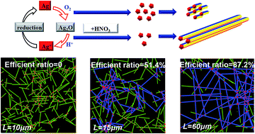
Combination between eqn (1), (4) and (5), the etching behavior as well as the cyclic reaction could also be well explained. Moreover, this could help to solve the awkward question met above by the first possible mechanism. Actually, concentration of O2 in the autoclave is limited, it was 2.7 mmol L−1, which is 11% of [Ag] (0.024 mol L−1) in the system. After consumption of O2 by few cycles, silver nanostructures could grow freely. When there was few amount of HNO3 pre-added, the consumption was accelerated, this is why no obvious nanostructure could exist at the first 5 hours (as shown in Fig. 2).
The newly proposed oxidative etching behavior could be simulated in Fig. 4. Based on such mechanism, nucleus could be screened thus only limited part of them could grow into longer nanowires. It should be acknowledged that, HNO3 showed oxidative nature to some extent. In experiment without addition of PVP, solution color changed little after reaction, and nothing was left at the bottom of centrifuge tube even though very high rate centrifugation (10k rpm/30 min) was used. As a result, less silver ions had been reduced. The appearance of silver nanostructures thus implies that PVP polymer chains have provided protection against oxidative etching. As a result, in the relatively low temperature reaction as described here, oxidative etching behavior was mainly exerted by O2 and acidic HNO3. Too high concentration is again not preferred due to slowed reacting rate brought by Le Chatelier's principle. Such effect could be well demonstrated by monitoring the remained Ag+ in the reaction. As shown in Fig. S1,† though reacted at same temperature and also same period, Ag+ has not been reacted completely in reaction with small amount of HNO3 pre-added.
![]() | ||
Fig. 4 Schematic of confined seeds nucleating process brought by HNO3, enhanced oxidative etching behavior and the application in growing very long AgNWs. |
The screen effect is very useful to synthesis very long AgNWs. Besides the solvothermal reaction, pre-addition of small amount of HNO3 could also help to achieve nanowires longer than 170 μm in one step polyol method (Fig. S3†). And in the time-controlled experiment at similar reacting period at 11 h, about 265 μm-long AgNWs were achieved with pre-addition of HNO3, which was 50 times longer than that W/O HNO3 pre-added, as depicted by Fig. S4.† The HNO3 assisted solvothermal reaction is different from the high pressure polyol method,15 which was high pressure reaction (100–150 psi, equaling to 6.8–10.2 atm) created by N2 along with high temperature heating (170 °C). It is easy to follow, especially for mass production.
The increased nanowire length is beneficial to improvement in optoelectronic performance of TCFs. As shown in Fig. 5(a), for TCFs made of longer nanowires (according to Fig. 1(d), average length of 138 μm) with transmittance decreased from 94.2% to 83.1%, Rsh decreased from 40.6 to 4.5 Ω sq−1. T% & Rsh of 92.1% (@550 nm), 12.6 ohm sq−1, and 89.5%, 9.2 ohm sq−1 were achieved. Such performance is slightly better than that reported in literature, at similar transparency (around 90%), the achieved Rsh was nearly 50% of that reported.17 Moreover, at similar Rsh, TCFs fabricated from longer nanowires were more transparent (>10%) than that using shorter ones (average length/width of 55.75 μm/237 nm), which is similar to that reported before.16 The performance is also comparable to the commercial ITO, but AgNWs TCFs showed much wider transmittance window, especially in two areas 350–600 nm and 900–1100 nm, which is appealing for optoelectronic applications.35 It is noted that, besides the improved nanowire length, thermal annealing also contributes to the improved film conductance. As could seen in Fig. S5,† welding was realized between neighboring AgNWs at intersecting area after annealing at 200 °C for 20 min, which is beneficial to the film conductance. However, longer annealing time causes broken nanowires (Fig. S5†), so does higher annealing temperature. In following sections, to better illustrate the effect of higher annealing temperature as well as nanowire length on conductance of AgNWs TCFs, stability-test experiment and simulation were performed.
In order to show the stability against heating, TCFs made of nanowires with two kinds of length distribution (short/long ones, SNWs/LNWs) were heated at open air and N2 respectively. As shown in Fig. 6(a), when treated in open air, nanowires were easily broken into short parts, which were due to oxidization by O2;36 While in N2, the nanowires turned to be made of several thicker rods separated by much thinner ones, but less of them were broken, even though they were heated at 360 °C for 0.5 h. The re-arrangement of silver atoms along nanowire length could be ascribed to the so-called Rayleigh instability.37 Nanowire length was collected and shown in Fig. 6(b), after heating, both SNWs/LNWs were cut down to be around 25 μm, which is one quarter (LNWs) or half (SNWs) of the starting length. But for long nanowires, there are more nanowires with length between 50 and 120 μm. The evolvement of morphology has drawn much effect on conductance of TCFs. As shown in Fig. 6(c), for TCFs treated in open air, sheet resistance increases quickly with temperature. For that made of short nanowires and high transparency (S88%), it even turned to be insulate. While for that treated in N2, film conductance changed slightly (Fig. 6(d)). Meanwhile, transparency also changed slightly, this once again shows that silver atoms have been just re-arranged along the nanowire length according to Rayleigh instability. In both of these two cases, LNWs performed better than SNWs in outputting relatively higher conductance. The stability test also implies that thermal annealing in protected gas environment is preferred for silver nanowire based TCFs.
From above discussion one could find that nanowire length (hence the aspect ratio) plays an important role in the conducting behavior of TCFs. In order to give more details about the effect, simulations were done based on Monte Carlo and Kirchhoff's circuit law.38,39 For each point, ten times of separated simulation were done, and the average (along with standard error) was used. Seeing from Fig. 7(a)–(c) one can find that, when nanowires are relative short (aspect ratio is small), for example 10 μm in average (aspect ratio of 40 in average), no conductive routes could be formed, thus the film is insulate. Then as it is 15 μm, conductive routes start to form stably, implying that the network is conductive.23 At this very point, 51.4% of total nanowire length becomes effective in form conduction routes, and the ratio increases further with nanowire length, which is reflected from Fig. 7(d). Besides the efficient ratio, film conductance is also improved by increment of the length, which relates closely to the efficient ratio. As shown in Fig. 7(e), sheet resistance of TCFs decreases quickly with increase of efficient ratio. The relationship between the two could be well understood by Kirchhoff's circuit law. As efficient ratio increases, more conductive routes are formed between the left/right boundaries of network, which cuts down the resistance between these two counter boundaries (as depicted in inset of Fig. 7(e)). It is also worthy noting that, only resistance from nanowire itself has been considered in the calculation, and the corresponding Rsh is 1.74 ohm sq−1, which is much smaller than the experimental value of 12.87 ohm sq−1. The gap between the two is from the contact resistance between neighboring nanowires.1,3,38,40,41
At last, the relative larger width came along with the ultra-long length was also caused by the oxidative etching processes, because nanowires larger in size were more stable when growing in corrosive background. But nanowire width could be further decreased through replacing Cl− by Br−,2 employing longer chain PVP polymers,15 as well as creating less oxidative etching background. For example, by replacing Cl− by Br−, we have recently synthesized silver nanowires with width from 30–90 nm, of which the detailed mechanism is under study.
Footnote |
† Electronic supplementary information (ESI) available. See DOI: 10.1039/c6ra20147d |
This journal is © The Royal Society of Chemistry 2016 |