Muhammad Sulamana,
Shengyi Yang*ab,
Taojian Songc,
Haowei Wangc,
Yishan Wangc,
Bo Hea,
Miao Dongd,
Yi Tangd,
Yong Songd and
Bingsuo Zoua
aBeijing Key Laboratory of Nanophotonics and Ultrafine Optoelectronic Systems, School of Physics, Beijing Institute of Technology, Beijing 100081, China. E-mail: syyang@bit.edu.cn; Tel: +86-10-68918188
bState Key Lab of Transducer Technology, Chinese Academy of Sciences, China
cBeijing Key Laboratory of Nanophotonics and Ultrafine Optoelectronic Systems, School of Materials Science and Engineering, Beijing Institute of Technology, Beijing 100081, China
dKey Lab of Photoelectronic Imaging Technology and System, Ministry of Education, School of Optoelectronics, Beijing Institute of Technology, Beijing 100081, China
First published on 7th September 2016
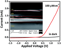
Semiconductor quantum dots (QDs) have been the subject for wide research studies owing to their quantum confinement effect. Photodetectors or photodiodes are recognized potential applications for QDs due to their high photosensitivity, solution processability and low cost of production. In this paper, a solution-processed near-infrared photodiode ITO/ZnO/PbSxSe1−x/Au, in which ternary PbSxSe1−x QDs act as the active layer and the ZnO interlayer acts as electron-transporting layer, was demonstrated. The photosensitive spectrum can be broadened by adjusting the molar fraction of ternary PbSxSe1−x QDs. The narrow band edge of absorption and photoluminescence exciton energy of PbSxSe1−x alloyed NCs were blue-shifted from the band edge of the same size PbSe QDs to the band edge of PbS QDs by controlling the S/(Se + S) molar ratio in the synthetic mixture. Efficient electron extraction was carried out by inserting a solution-processed ZnO interlayer between the indium-tin oxide (ITO) electrode and the active layer. Our experimental results show that the solution processing of the ZnO layer can lead to high-performance photodiodes by using photosensitized PbS0.4Se0.6 alloyed nanocrystals as the active layer. The effect of the thickness of the active layer on the device performance was briefly described and a maximum photoresponsivity and specific detectivity of 25.8 A/W and 1.30 × 10¹³ Jones, respectively, were obtained at a certain thickness under 100 μW cm−2 980 nm laser illumination. The devices are made stably by layer-by-layer ligand exchange treatment.
Photovoltaic devices made by ternary nanocrystals are much efficient than those based on either pure PbSe or pure PbS CQDs.9 The progress in photodetecting devices has opened new applications for IV–VI compounds. The photodiodes based on lead chalcogenides and their alloys are important sources for the tunable radiations in the near and mid-infrared wavelength region. Ternary alloys prepared out of binary semiconductors can thus be grouped as a class of semiconductors in which lattice parameter, band-gap and other operational parameters could be continuously varied as per requirement by selecting binary constituents and their relative concentrations suitably.12 Ternary semiconductor CQDs thus provide a possibility of tailoring their properties as per requirements and hence project themselves as important semiconducting materials for future advancements in device fabrication.13,14
Unique optical and electrical properties of ternary PbSxSe1−x alloyed semiconductors as compared to the other IV–VI semiconductors (PbSe or PbS), such as high quantum efficiency, narrow band-edge, and fast response time, refer them for widely used for solar cells and near infrared photodetectors.15–21 However, only a few papers reported ternary PbSxSe1−x NCs with narrow size distribution, synthesized in different experimental conditions and the colloidal procedures for preparing ternary PbSxSe1−x core-alloyed shell CQDs as a promising photoactive material in IR photodetectors and their usage in photovoltaic devices, as compared with binary PbS or PbSe.22–24 In this paper, high quality PbSxSe1−x alloyed CQDs with variation of the chemical composition were synthesized and have been incorporated for high performance near infrared photodetector ITO/ZnO/PbSxSe1−x/Au utilizing a ZnO interlayer between ITO and active layer,25 which also removes the prerequisites of poly(3,4-ethylenedioxythiophene):poly(styrene-sulfonate) (PEDOT:PSS) film as a modification layer, which has been shown to introduce morphological and chemical instabilities at the interface with ITO.26,27 ZnO is an n-type material and its work function is close to the conduction band of PbSxSe1−x, also the electron mobility of ZnO interlayer is high, so the electron extracted from active layer can quickly transfer to the ITO. The structural, optical and electrical properties have been investigated for both the variable chemical composition PbSxSe1−x alloyed CQDs and solution-processed ZnO interlayer. The highest responsivity and maximum specific detectivity of 25.8 A W−1 and 1.30 × 10¹³ Jones, respectively, have been achieved for IR photodiode ITO/ZnO/PbS0.4Se0.6/Au under 100 μW cm−2 980 nm laser illumination.
The absorption spectrum of CQDs and ZnO thin film were measured with an ultraviolet-visible-near infrared (UV-vis-NIR) spectrophotometer (Shimadzu, UV-3600). Electrical and photoresponse characteristics of the devices were measured using a Keithley semiconductor characterization system (Model 4200-SCS) in dark and under 980 nm laser illumination. The transmission electron microscopy (TEM) images of the CQDs were taken using Tecnai G2 F20 U-TWIN. The X-ray diffraction spectrum of the CQDs was characterized by Rigaku RM-2000.
![]() | ||
Fig. 1 TEM image of PbS0.4Se0.6 CQDs. Inset presents the HRTEM image of synthesized QDs, implying its average size of ∼5 nm. |
In order to study the structural properties of ZnO thin film, XRD and scanning electron microscopy (SEM) has been performed. Fig. 3b demonstrates the XRD pattern of ZnO thin film which is exactly matched with XRD of bulk ZnO reported previously.31 From here, one can easily see that the growth of solution-processed ZnO thin film on glass/ITO substrate by spin-coating was successfully verified and the grown ZnO thin film is in the nanoscale size which was confirmed by XRD. The absorption and photoluminescence (PL) spectra of thin film are shown in Fig. 3c which is almost similar to previously reported absorption and emission spectra of ZnO but with a little shifting.31–33 Here, PL spectrum of ZnO nanocrystals spin-coated on glass substrate in Fig. 3c, showing UV emission peak at about 387 nm, corresponds to the near-band-edge emission of ZnO nanocrystal. Also, an intensive broad visible emission band (around 450 nm) due to defects or impurities is observed. This broad emission is normally detected in ZnO bulk and nanostructures34–36 and it may be due to the oxygen vacancy as the defect.36
Fig. 3d presents the scanning electron microscope (SEM) image of ZnO thin film on glass substrate. All the above evidences justified that the solution-processed thin film was pure ZnO in nanoscale size which can be utilized to get high performance IR photodiodes. In order to confirm the purity of PbS0.4Se0.6 CQDs we have studied the structural and optical properties of the synthesized PbS0.4Se0.6 nanocrystals. Fig. 4 shows the absorption spectrum of PbS0.4Se0.6 CQDs, the absorption peak locates at 1140 nm. Also, the XRD pattern of PbSxSe1−x are shown in the inset of Fig. 4. The intensity peaks in XRD pattern of the ternary CQDs are exactly matched with that of the bulk PbS and PbSe, which reveals that the ternary PbS0.4Se0.6 CQDs were really alloyed and crystalline. The absorption spectra of PbSxSe1−x with the variation of precursor “S” and the blue-shift were investigated by increasing the ratio of S which was reported in our previous paper.28
![]() | ||
Fig. 4 Absorption spectra of PbS0.4Se0.6 CQDs. Inset presents the XRD pattern of synthesized QDs with JCPDS card of bulk PbS and PbSe. |
Also, the absorption spectrum of the PbS0.4Se0.6 nanocrystals achieved after different interval of time proves that the synthesized nanocrystals are very stable and can be used for a long time,28 furthermore, the lifetime of the fabricated devices utilizing the photosensitized CQDs can be enhanced. Blue-shift was observed by increasing the concentration of S precursor in PbSxSe1−x alloy so that one can see that the absorption spectra can be extended into near IR by adjusting the ration of S and Se precursors.
In order to get high device performance, we fabricated a photodiode ITO/ZnO/PbS0.4Se0.6/Au (see Fig. 3a), in which an interlayer of ZnO between the ITO and the active layer is to extract the electron from the device, as reported previously.25 The main limiting factor for the device performance of the CQDs-based photodetectors is the high dark current due to the narrow band-gap and the high density of states. A disadvantage of PbSe CQDs is their poor stability in ambient air and they can be destabilized easily, due to which their applications are limited.37 Therefore, in order to increase the interparticle coupling and carrier mobility, longer insulating oleate ligands should be exchanged by shorter and more conductive surfactants such as ethandithiol (EDT) and/or 3-mercaptopropionic acid (MPA).38,39 Therefore, EDT treatment has been selected in our experiments to remove the long insulating ligands.
To determine the photoresponse capability of the device, we explored its photosensitivity dependence on laser illumination intensities using 980 nm laser. Fig. 5a shows the I–V characteristics of the fabricated device in dark and under 100 μW cm−2 illumination intensity of 980 nm laser while I–V characteristics at other illumination intensities are illustrated in Fig. 5b. Under IR illumination the photocurrent increases drastically, particularly at higher applied voltage which demonstrates an asymmetrical and non-linear I–V behavior of the photodiode. The inset of Fig. 5a presents the I–V curves in dark which verifies that the typical diode behavior of fabricated device. From here one can see that the photocurrent increases by increasing the illumination intensity and become saturated by further increasing illumination intensity which is further illustrated in Fig. 6, which shows that the photocurrent vs. the illumination intensity, the current density vs. the applied voltage in dark and under IR illumination is illustrated by the inset in Fig. 6, implying that the device is photosensitive and it shows good photoresponse under IR illumination. This enhanced photocurrent under IR illumination is attributed to the strong absorption of CQDs, CQDs absorb photons and photogenerated carriers occur and then they transfer to the ZnO interlayer after excitons disassociation. Most importantly, here ZnO will not be responsible for the photon absorption in near IR region, however, the active layer of photosensitized nanocrystals will absorb the photon and photogenerated carriers will be extracted by the ZnO layer due to the electron–hole pair generation and quickly transferring to the ITO. Therefore, the ZnO layer plays an important role by blocking the holes and by minimizing the work function between the carrier collector and the active layer.
![]() | ||
Fig. 6 Photocurrent vs. illumination intensity using 980 nm laser. Inset shows the current density vs. applied voltage in dark and under illumination. |
The high photocurrent implies the efficient electrons and holes extraction by the electrodes. In fact, the working principle of our device, ITO/ZnO/PbS0.4Se0.6/Au, can be explained using energy band diagram. The conduction band level and the valance band level of PbS0.4Se0.6 QDs and can be determined using cyclic voltammetry (not shown here), and they are −4.22 eV and −5.53 eV for PbS0.4Se0.6 and −4.35 eV and −6.89 eV for ZnO respectively. For chemically stable materials, their valance bands should be completely filled and the charge transportation occurs only in the partially filled states since they can accept or donate electrons easily. Fig. 7 presents the energy band diagram for the photodiode ITO/ZnO/PbS0.4Se0.6/Au. From here, one can see that electron transfer from PbS0.4Se0.6 to the ZnO interlayer does not result in a significant loss in energy, implying that the LUMO of PbS0.4Se0.6 is very close to the conduction band of ZnO at −4.35 eV with an energy difference of 0.13 eV. Hence, the electrons can be extracted by ZnO interlayer and can easily transport to the ITO while holes can be blocked by ZnO interlay, this is also the reason why we can get high photocurrent with low illumination intensity (see Fig. 5). High JSC in the device indicates that the Au electrode acts as an efficient hole-collecting electrode. Based on the efficient hole-collecting nature of the PbS0.4Se0.6/Au interface is evident that a shift from vacuum occurred upon contact of the two materials with an energy difference of 0.4 eV. Regardless of apparent limitations in stability, this hetero-junction device provided here has several important consequences for photovoltaic devices.
In order to calculate the photoelectric properties of ITO/ZnO/PbS0.4Se0.6/Au photodiode, we selected a lower illumination intensity of 100 μW cm−2 in our experiments. The first and most important feature of the photodetector is the sensitivity which can be calculated by eqn (1). The photosensitivity (K) of the photodetector is simply defined as “the capability of a photodetector to distinguish an incident optical signal from noise”,40,41 and it is defined as
![]() | (1) |
Photoresponsivity (R) and specific detectivity (D*) are the key factors for characterizing the performance of the photodetectors.42,43 The photoresponsivity is the measure of its sensitivity to light and it is defined as the ratio of the photocurrent to the incident illumination intensity, i.e. R = Iphoto/Pill, where Iphoto = Iill − Idark and Pill is the incident illumination power intensity. A high photoresponsivity of 25.8 A W−1 was obtained under 100 μW cm−2 980 nm laser at applied bias of −1.5 V. The specific detectivity is another important factor for evaluating the device performance of a photodetector, and it can be determined by eqn (2),
![]() | (2) |
The photocurrent of the device was determined by the recombination efficiency of electron–hole generated in photoactive layer and balanced between bottom and top electrodes. The thickness of the active layer is critical to get high photoresponse. To examine the effect of the thickness of QDs layer on device performance we varied the number of QDs layers by spin-coating and using ligand exchange after each layer. Use of ligand exchange in this way, not only helps to protect the previous layer from damaging the next layer by spin-coating, resulting the increment of the thickness, also the stability of CQDs can be enhanced. We fixed the thickness of the ZnO interlayer at ∼120 nm and the thickness of the PbSxSe1−x CQDs layer was varied from 150 nm to 350 nm by a step of 50 nm. Table 1 shows the important parameters of the device which rationalizes the device performance by using 100 μW cm−2 980 nm laser illumination. The device having lowest thickness of active layer exhibits the low photoresponse which justifies the discrepancy of carriers' results in insufficient recombination of electron–hole regenerated at the interface of active layer and carrier collecting layer. This low photoresponse may also due to the high leakage current, to overcome this leakage current and get sufficient recombination of electron–hole pairs, the thickness of the QDs layer was increased by spin-coating and obtained a high photoresponse at the thickness of ∼300 nm accordingly because more photo-generated carriers can be obtained in the photoactive layer which leads to more electron–hole recombination. This high performance of the photodiode is due to the high photocurrent which was produced due to the high recombination efficiency of photo-generated carriers at the interface of ZnO interlayer and PbS0.4Se0.6 CQDs. For the sake of confirmation of device stability we re-characterized the device for its photocurrents in dark and under illumination after 30 days and obtained almost same results, as shown in Fig. 8, implying the device is very stable.
Thickness (nm) | Photosensitivity K | Photoresponsivity R (A W−1) | Specific detectivity D* (Jones) |
---|---|---|---|
150 | 1.8 | 0.05 | 4.11 × 10⁹ |
200 | 22.6 | 2.95 | 4.48 × 10¹¹ |
250 | 6.19 × 10² | 5.77 | 3.34 × 10¹² |
300 | 2.11 × 10³ | 25.8 | 1.30 × 10¹³ |
350 | 1.14 × 10³ | 24.6 | 1.10 × 10¹³ |
The better device performance forternary nanocrystals is due to a combination of material properties as well as a redistribution of the trap states which origins from ligand exchange and potentially damage during depositing metal.44–46 To get the higher electron mobility, the grain size of the electron-transporting layer should be small enough and crystalline (e.g. nanocrystals), as discussed in the above, the photoexcited electrons can easily transport to the ZnO layer due to the nanoscale size of the ZnO nanocrystals, and then electrons can easily transfer to the ITO electrode. Since the grain-size of the ZnO film is in the domain of nanoscale, the electron mobility of the device gets larger. Therefore, the electrons can transfer from the active layer to ZnO and quickly transport to ITO. The higher current produced by PbS0.4Se0.6, may arise from a significantly larger exciton Bohr radius than that of PbS due to the integration of Se. The larger Bohr radius established greater electronic coupling between nanocrystals and delocalizes the carriers, which can reduce the effects of nanocrystal surface traps and therefore charge transportation gets higher.
According to the Schottky junction theory, the barrier height of an ideal metal semiconductor contact is determined by the relative position between metal work function and semiconductor Fermi energy.47 The size dependent conduction and valence band-edge of PbS and PbSe nanocrystals have recently been measured and PbS is reported to have energy levels closer to vacuum energy than PbSe. One major limitation in practical Schottky junctions is that the barrier height can't exceed the half of the band-gap. Otherwise, the minority carrier density would be larger than the majority carrier density at the junction, thus forming an inversion layer.48 In this circumstance, the true limit of the barrier height is directed by the difference between the intrinsic level and the Fermi level of the nanocrystal film, in this way, the work function of the metal contact will be closer in energy to vacuum than the intrinsic energy of the semiconductor. The density of the trap states within the band-gap is most likely due to the differing voltages of the materials. Since the trap states are closely related to the Fermi levels, the position and density trap states at the surface in PbS, PbSe and PbSxSe1−x may vary because of various surface energies of the binary phases to the ternary, and the relative position of the Fermi level to the valance band edge of the active layer could be determined by this difference.
The ternary nanocrystals with optimum photovoltaic properties and tunable composition can be obtained by alloying, and it was demonstrated to be a successful approach. Due to their larger excitons Bohr radius, lead chalcogenides are appropriate materials to fabricate high-performance devices. Therefore, alloying demonstrates to be a very easy and operative method to get the NCs with appropriate band-gap and surface passivation by the advantages of the counterparts of the binary compounds. The solution processed ZnO inter-layer efficiently blocks holes and collects electrons from the PbSxSe1−x, the requirement of vacuum processing is not necessary, the thin film can be fabricated using inexpensive materials, and the need of PEDOT:PSS can also be removed. The Au electrode is air-stable and offers the possibility of a laminated back contact. The improvements established by this investigation are not restricted to the PbSxSe1−x active layer, more air-stable replacements could easily be incorporated into this configuration.
This journal is © The Royal Society of Chemistry 2016 |