Improved performance in Ag2S/P3HT hybrid solar cells with a solution processed SnO2 electron transport layer
Yaxiong Guoa,
Hongwei Leia,
Borui Lia,
Zhao Chena,
Jian Wena,
Guang Yanga and
Guojia Fang*ab
aKey Laboratory of Artificial Micro- and Nano-Structures of Ministry of Education of China, School of Physics and Technology, Wuhan University, Wuhan 430072, PR China. E-mail: gjfang@whu.edu.cn
bWuhan University, Suzhou Institute, Suzhou 215123, PR China
First published on 10th August 2016
Abstract
We successfully constructed a heterojunction structure composed of Ag2S nanocrystals/P3HT conjugated polymer with a relatively high absorption coefficient and broader absorption from the ultraviolet to near-infrared region. The assembled P3HT:Ag2S devices exhibited outstanding short-circuit current density around 19 mA cm−2. Meanwhile, we demonstrated that a low-temperature solution-processed nanocrystalline SnO2 thin film prepared by a facile synthesis method can be an excellent electron transport layer (ETL) material for hybrid solar cells. The SnO2 based hybrid solar cells exhibit an open circuit voltage of 280 mV, which was 100 mV higher than those for devices without SnO2. Based on the above work, we hypothesized that the higher power conversion efficiency is due to the excellent properties of nanocrystalline SnO2 films, such as high electron mobility and excellent transparency at visible wavelength and enhanced exciton dissociation efficiency, and better energy level alignment between FTO and Ag2S for greater photovoltage retention. The simple low temperature low energy consumption, and low-cost soft-chemical process is compatible with the roll-to-roll manufacturing of low-cost hybrid solar cells on flexible substrates.
1. Introduction
Hybrid solar cells based upon an organic–inorganic semiconductor heterojunction are currently the theme of significant interest as they incorporate the attractive properties of both organic and inorganic materials. Hybrid solar cells utilize the advantages of the organic – enhanced light absorption in a wide range of wavelengths, adjustable molecular structures for energy band alignment, and use the advantages of inorganics, including facile solution process synthesis ability, high carrier mobility and compatible fabricating processes, and so on.1–7Monoclinic α-Ag2S is an attractive material for use in photovoltaic devices due to its appropriate narrow band gap of 1.1 eV, a relatively high absorption coefficient from the ultraviolet (UV) to near-infrared (NIR) region, and excellent optical limiting properties. Therefore, it has also been used in a wide range of applications in optical and electronic devices such as photoconductive cells, infrared detectors, superionic conductors and solar-selective coatings. In addition, Ag2S is reported to have negligible toxicity in organisms.8–11
The development of Ag2S photovoltaics (PVs) is limited by low device open-circuit voltages. A strong contributing factor to this underperformance is charge recombination can easily happen between Ag2S and cathode. Therefore, it is highly desirable to develop an approach toward easy fabrication, low-cost and high-efficiency planar Ag2S solar cells. Promising heterojunction candidates SnO2, which demonstrate slightly positive conduction-band offsets and high VOC potential. Tin oxide (SnO2) is a promising wide band gap oxide material because of its higher electron mobility and large band gap (3.8 eV). Mobility reported in both single crystal SnO2 (μe ∼ 250 cm2 V−1 s−1) as well as nanostructures (μe ∼ 125 cm2 V−1 s−1) are orders of magnitude higher than other possible candidates like ZnO and TiO2. Furthermore, SnO2 has a low sensitivity to UV degradation due to its larger band gap and hence has better long term stability.12–15
In this study, we have fabricated hybrid cells with FTO/Ag2S/P3HT/Au and FTO/SnO2/Ag2S/P3HT/Au configurations. Solution-processed SnO2 was introduced between FTO and Ag2S to explore the electron transport effects on the device performance. A remarkable enhancement of the device efficiency is found upon inserting a SnO2 layer, dominantly explained by enhanced exciton dissociation efficiency or the reduction of the energetic barrier at the FTO/Ag2S interface. Upon inserting a SnO2 layer, the PCE increases from 1.1% to 2.1%, resembling an improvement of app. 90%.
2. Experimental details
2.1. Material
Silver target was purchased from Beijing InnoChem. Sulfur powder (99.99%) was bought from Aladdin Reagent. The polymer donor P3HT was bought from Rieke Metals. Tin chloride dehydrate (SnCl2·2H2O) were purchased from Sinopharm Chemical Reagent Co., Ltd. (China). All of the used reagents were analytical grade, without further purification. The purity of the gold top anode prepared by thermal evaporation was 99.99%. Fluorine-doped tin oxide (FTO) coated glass with a sheet resistance of 14 Ω sq.−1 was purchased from Asahi Glass (Japan).2.2. Preparation of light harvesting layer Ag2S
The FTO substrate was cleaned by ultrasonic treatment in detergent, deionized (DI) water, acetone, and alcohol sequentially for 10 min each. Then, the FTO substrate was dried by N2 gas. Finally the cleaned substrate was treated in an UV-ozone chamber for 15 min. Silver film was prepared by a radio frequency (RF) magnetron sputtering system using a metal silver (99.99% pure) target in Ar atmosphere. The base vacuum chamber was pumped down to a pressure below 10−4 Pa. The Ar gas flow rate was retained at 10 standard-state cubic centimeter per minute (sccm). The deposition progress was carried on under a pressure of 1 Pa at 60 °C and RF power of 60 W. By controlling the sputtering time, we could achieve copper films of various thicknesses.In a typical procedure, the elemental silver coated FTO glass and 0.01 g sulfur powders were put into a 80 mL vessel, and then 20 mL of N,N-dimethylformamide (DMF) was added. The container was maintained at 80 °C for 6 h. After it cooled down to room temperature naturally, the FTO with the product was taken out of the autoclave and washed with ethanol for several times. Then the FTO/Ag2S was dried in an oven at 60 °C for 30 min. Finally, a black thin film on the FTO substrate was obtained.
2.3. Solar cells fabrication
SnO2 precursor solution was prepared by dissolving tin chloride dehydrate (SnCl2·2H2O) in ethylene glycol by stirring for several hours at a concentration of 5–40 mg per 2 mL to serve as a stock solution. The cleaned substrate was treated by oxygen plasma right before use. In SnO2 devices, the SnO2 precursor solution was spin-coated onto the FTO glass at 2000 rpm for 60 s. Afterwards, the samples were annealed at 200 °C in an air atmosphere for 2 h. The synthesized SnO2 ETLs were treated by UV-ozone for 15 min before magnetron sputtering deposition of silver film. The Ag2S was deposited on the substrates as above described. After the typical hydrothermal process, the substrates was dried at 60 °C in a vacuum oven overnight. The P3HT solutions (17 mg mL−1 in chlorobenzene) were spin-coated onto Ag2S/SnO2/FTO film at 1500 rpm for 40 s and subsequently annealed in N2 atmosphere at 100 °C for 10 minutes and the Au counter electrode was finally deposited by a thermal evaporator under a pressure of 1 × 10⁻³ Pa. The active area of the device was fixed at 0.03 cm2.2.4. Device characteristics
The current density–voltage (J–V) characteristics of the PSCs were measured on a CHI660D electrochemical workstation (ShangHai, China) with a scan rate of 100 mV s−1 and the device test was carried out under illumination of AM 1.5G, 100 mW cm−2 (The light intensity was calibrated using a Si photodiode) at room temperature using a solar simulator.The crystal structure of the Ag2S film was evaluated by X-ray diffraction (XRD) with a Bruker D8 Advance diffract meter using Cu Kα radiation at 40 kV and 40 mA. Line traces were collected over 2θ values ranging from 20° to 80°.
The morphology of hybrid solar cells were observed by a high resolution field emission scanning electron microscope (SEM, FEI XL-30). The thicknesses of the Ag2S were also measured by SEM observation. The energy dispersive spectroscopy (EDS) measurement was made in a scanning electron microscope (FEI XL-30) equipped with an X-ray analyzer and an EDS spectrometer.
The square average roughness (RMS) of the SnO2 films and bare FTO substrates were characterized by an atomic force microscopy (AFM, SPM-9500j3). The transmission and absorption spectra were measured by an ultraviolet-visible (UV-vis) spectrophotometer (CARY 5000, Varian) at room temperature.
X-ray photoelectron spectroscopy (XPS) analyses and ultraviolet photoemission spectroscopy (UPS) were performed on an ESCA Lab220i-XL electron spectrometer (VG Scientific) using a monochromatic Al Kα source (300 W).
The compositions and chemical states of the Ag2S films and the SnO2 ETLs were examined by XPS. Before been tested, samples were sputtering cleaned, to remove atmospheric contamination in the XPS chamber for approximately 30 s, by the lower energy of Ar+, and the Ar+ gun was operated at 0.5 kV, at a pressure of 1 × 10⁻⁷ Pa. The vacuum pressure of the analysis chamber was better than 1 × 10⁻⁸ Pa. The whole survey scan to identify the overall surface composition and chemical states were performed, using a monochromated Al Kα X-ray source (=1486.68 eV), detecting photoelectrons at a 150 eV pass energy and a channel width of 500 meV. The surface carbon signal at 284.6 eV was used as an internal standard.
The work function and band energy position were calculated by UPS measurement. UPS was carried out under a pressure of ∼2 × 10⁻¹⁰ Pa using helium Iα (21.22 eV) radiation from a discharge lamp operated at 90 W, a pass energy of 10 eV, and a channel width of 25 meV, and the energy resolution was 0.02 eV. A −9 V bias was applied to the samples, in order to separate the sample and analyze low-kinetic-energy cutoffs.
3. Results and discussion
3.1. Characterization of light absorber Ag2S
Fig. 1(a) and (b) show the device structure of the hybrid solar cells and the typical XRD pattern of Ag2S film on FTO substrates, respectively.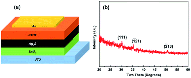 | ||
| Fig. 1 The device structure and the XRD pattern of the Ag2S films, which shows a monoclinic α-Ag2S phase of the synthesized films from the hydrothermal progress. | ||
The phase identification of as-synthesized Ag2S films was performed using XRD measurement presented in Fig. 1(b). The peaks at 30.2°, 35.5°, and 51.6° 2θ correspond to the (111), (![[1 with combining macron]](https://www.rsc.org/images/entities/char_0031_0304.gif) 21), and (
21), and (![[2 with combining macron]](https://www.rsc.org/images/entities/char_0032_0304.gif) 13) reflections of monoclinic α-phase structured Ag2S, respectively (JCPDS, 14-72).16–18
13) reflections of monoclinic α-phase structured Ag2S, respectively (JCPDS, 14-72).16–18
In order to study the morphology and confirm the end product of our hydrothermal synthesis, the scanning electron microscopy (SEM), EDS, XPS and UPS measurements were carried out. By varying the sputtering time of Ag target, we achieved Ag2S films of different thicknesses.
The film morphology and chemical composition were determined by scanning electron microscopy (SEM) and energy dispersive spectroscopy (EDS) in Fig. 2. Fig. 2(a) is a low magnification SEM image of the initial magnetron sputtered Ag. Well distributed particles of nanosized elemental silver grains with little size (about 60–80 nm in diameter) can be observed. The insert of Fig. 2(a) is an AFM image of the original magnetron sputtered Ag surface which was assembled by nanosized elemental silver grains. Fig. 2(b) shows typical SEM images of the as-prepare Ag2S nanocrystal thin film obtained after 6 h of reaction with elemental sulfur at 80 °C. The SEM image of the Ag2S thin film at low magnification reveals that the selected area of the FTO glass is fully covered with ordered Ag2S nanocrystals. The nanocrystals have nonuniform diameters in the range of 60 to 150 nm. The insert of Fig. 2(b) is a SEM image of the vertical section of the Ag2S film, showing that the mean thickness of the Ag2S film is about 400 nm. Fig. 2(c) shows the SEM image of the fabricated P3HT/nanocrystals Ag2S hybrid film. As we expected, the P3HT polymer is smooth and neatly infiltrate into the nanopores between adjacent Ag2S nanocrystalline. The thickness of the fabricated P3HT film was also measured to be about 100 nm using cross-section SEM images of the film. The EDS spectrum in Fig. 2(d) of the Ag2S films shows strong silver and sulfur signals with Ag![[thin space (1/6-em)]](https://www.rsc.org/images/entities/char_2009.gif) :
:![[thin space (1/6-em)]](https://www.rsc.org/images/entities/char_2009.gif) S ratios of 2.16
S ratios of 2.16![[thin space (1/6-em)]](https://www.rsc.org/images/entities/char_2009.gif) :
:![[thin space (1/6-em)]](https://www.rsc.org/images/entities/char_2009.gif) 1.00, which proves that the atomic ratio of elemental silver and sulfur is approximately 2
1.00, which proves that the atomic ratio of elemental silver and sulfur is approximately 2![[thin space (1/6-em)]](https://www.rsc.org/images/entities/char_2009.gif) :
:![[thin space (1/6-em)]](https://www.rsc.org/images/entities/char_2009.gif) 1.
1.
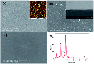 | ||
| Fig. 2 (a) SEM images of Ag films made on FTO substrates. (b) SEM images of Ag2S films after hydrothermal progress. (c) SEM images of P3HT films spin-coated on Ag2S substrates. (d) The EDS spectrum of FTO/Ag2S. The inset of Fig. 2(a) and (b) is the AFM images of Ag films made on FTO substrates and the cross-sectional SEM image of FTO/Ag2S respectively. | ||
The UV-vis-NIR absorption spectrum of a pristine P3HT film, Ag2S film and P3HT/Ag2S hybrid film are shown in Fig. 3(a). The pristine P3HT film exhibits the characteristic absorption spectrum ranging from 400 to 650 nm (Fig. 3(a), red curve). Meanwhile, the appearance of a broad absorption feature (320–750 nm) is observed, which is consistent with the presence of Ag2S (Fig. 3(a), blue curve). Fig. 3(b) depicts the NIR absorption spectrum of pure Ag2S film. A discernible absorption onset was detected in the NIR window at 1100 nm. As compared to bulk silver sulfide (Eg = 1 eV), the absorption spectrum of as-prepared films exhibits a large blue-shift, which suggests that the nanocrystalline behave within the quantum confined regime.19,20 The another explanation is that different aggregate nanocrystalline sizes contribute different absorption sub-bands.21,22
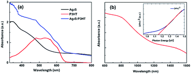 | ||
| Fig. 3 The UV-vis-NIR spectra of Ag2S films (a) (1) pristine P3HT thin film; (2) Ag2S thin film; (3) P3HT:Ag2S hybrid thin films. (b) The absorption curve of Ag2S thin film between 600 and 1600 nm. The inserted curve reveals the diagram of (αhν)2 against hν calculated from Fig. 3(b). | ||
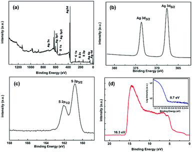
To investigate the basic properties of Ag2S individually, we prepared Ag2S films on silicon substrates for XPS characterization. The results are presented in Fig. 2. The binding energy of the spectra is calibrated by the C 1s peak of the aliphatic carbons at 284.6 eV as reference. Part of the oxygen in the spectra was attributed to adsorbed gaseous molecules. The XPS survey spectrum of Ag2S is shown in Fig. 4. Fig. 4(a) shows a whole scale scan of the results of XPS test where we can find the peaks of silver and sulfur. The peaks at 367.74 and 373.68 eV in Fig. 4(b) could be assigned to the binding energies of Ag 3d5/2 and Ag 3d3/2, respectively. The doublet feature of the Ag 3d spectrum is due to the spin–orbit separation.23,24 The spectrum of S 2p shown in Fig. 4(c) could be described as three peaks located at about 160.7 and 161.9 eV, respectively. The peaks at 160.7 and 161.9 eV could be assigned to the binding energies of S 2p3/2 and S 2p1/2, correspondingly, which were separated by a spin–orbit splitting of 1.2 eV.25,26
In order to understand the band alignment of Ag2S. UPS measurements were conducted to assist with determining the work function (WF) and ionization potential (IP) of the Ag2S. UPS measurement was carried out with the same machine using helium Iα as the ultraviolet source. The wavelength of the ultraviolet is 58.13 nm and the energy is 21.22 eV. The work function of the Ag2S is calculated by the following equation: EK = hν − EB, where EK means the kinetic energy. We can conclude from Fig. 4(d) that the binding energy (EB) is 16.3 eV. Thus, The WF of the Ag2S film is determined to be 4.9 eV. The insert of Fig. 4(d) shows the energy difference between the top of valence band (EV) and the Fermi level, which shows that EV is 0.7 eV below the Fermi level. The IP is defined as the energy difference between valence band edge and vacuum level, which is 5.6 eV. The optical band gap is determined by a Tauc-plot analysis of the absorption spectra by the following equation: (αhν)2 = A(hν − Eg), where Eg is the optical band gap of the samples and A is a constant.27,28 The value of the bandgap of the Ag2S film is estimated to be 1.1 eV. The electron affinity of the film was calculated to be 4.5 eV.
3.2. Study of simple planar Ag2S solar cells
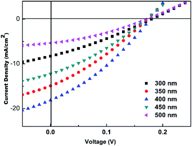
The effect of Ag2S film thickness on device performance was systematically characterized. Typical J–V curves for the five conditions are shown in Fig. 5 and its parameters are given in Table 1, where the Ag2S film were fabricated with different film thicknesses (300, 350, 400, 450 and 500 nm). Meanwhile, in our device, photogenerated carriers separate at P3HT/Ag2S p–n junction interface. Electrons are injected into Ag2S and are collected by FTO. Holes flow to the back side and are collected by Au contact. From the summarized device parameters chart in Fig. 5, Ag2S films with 300 nm thick exhibited poor open circuit voltage (JSC) and slightly lower fill factor (FF). When increasing film thickness to 350 nm, the JSC was improved from 8.3 to 14.9 slightly. This illustrates that slight further increase the thickness of light harvesting layer Ag2S benefits for the JSC. However, excessive Ag2S film thickness will reduce the device efficiency in the hybrid solar due to the separated exciton will be caught by defects in Ag2S film and will induce larger series resistance which all contributed to the lower JSC. The series resistance (Rs) raised from 13.5 Ω cm 2 to 21.9 Ω cm 2 which can also explain this phenomenon.29,30 The highest PCE was achieved for the Ag2S film when thickness is 400 nm. For film thickness less or greater than 400 nm, the device performances were degraded. The optimal devices show a VOC of 0.18 V, a JSC of 18.1 mA cm−2, a FF of 33.5%, and a PCE of 1.1%.| Ag2S thickness (nm) | VOC (V) | JSC (mA cm−2) | Rs (Ω cm2) | FF (%) | PCE (%) |
|---|---|---|---|---|---|
| a There are 12 samples for each device in this study. The errors of PCEs are ±0.1%. | |||||
| 300 | 0.18 | 8.28 | 17.5 | 29.2 | 0.43 |
| 350 | 0.18 | 14.93 | 14.1 | 29.1 | 0.78 |
| 400 | 0.18 | 18.16 | 13.5 | 33.5 | 1.10 |
| 450 | 0.18 | 12.25 | 14.9 | 29.6 | 0.65 |
| 500 | 0.18 | 5.37 | 21.9 | 31.6 | 0.31 |
3.3. Study and characterization of low-temperature solution-processed SnO2
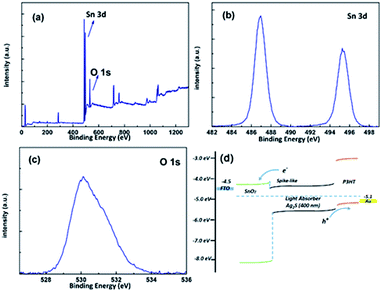
The SnO2 solutions prepared as described were spin coated onto UV-ozone pre-treated FTO substrates and annealed at 200 °C for 2 hours in air.X-ray photoemission spectroscopy (XPS) was performed to further investigate the surface characteristics of the SnO2 films. Fig. 6 shows a full scan spectrum of the SnO2 film made from the 0.1 M solution. O 1s and Sn 3d peaks are characteristic of SnO2. The full XPS spectrum survey given in Fig. 6(a) shows the presence of O and Sn. The binding energies of 487.11 and 495.56 eV correspond to the Sn 3d5/2 and Sn 3d3/2 peaks, respectively (Fig. 6(b)). The main binding energy of 531.06 eV is attributed to the O 1s, which is the O2− state in SnO2 (Fig. 6(c)). The higher binding energy can be assigned to the chemisorbed oxygen atoms or hydroxyl groups.15,31,32 Integrating the peaks and correcting for XPS sensitivity and emission efficiencies allows us to determine the quantity of remaining chloride in the sample to be approximately [Cl]/[O + Cl] ≈ 4.7 at%, indicating that more than 95% of the anions in the material has been successfully converted to oxygen. Moreover, the Sn 3d5/2 peak is symmetric and no shoulder is observed, which indicates that the film consists mostly of SnO2. The XPS spectrum for the SnO2 film made from the 0.1 M solution was found to be identical to that from the 0.02 M solution. Therefore, all films fabricated from solutions of different SnO2 concentrations are considered to have the same SnO2 composition. According to the XPS spectra and the literature report, the energy level diagram of hybrid solar cells with SnO2 ETL is shown in Fig. 6(d). The elevated conduction band minimum (CBM) contributes to the increase of the VOC. The upshifted CBM of the blocking layer is more compatible with the FTO and the light harvesting layer, reducing the energy loss through the electron transportation. Meanwhile, the downshifted valence band maximum (VBM) also could be more effective to block holes, resulting in less recombination of electrons and holes at the film surface and thus, giving a better FF.33
Fig. 7 presents the transmission spectra of SnO2 samples on FTO used in our work and bare FTO substrates. As we know, SnO2 is a wide band gap semiconductor, which has a strong absorption at short wavelengths. So we can see the SnO2 sample is more transparent than the bare FTO between 300 and 600 nm. This is an encouraging result since high transparency of electrodes is vital for photovoltaic devices. The variation of (αhν)2 versus hν are shown in Fig. 7 insert has been evaluated by extending the linear portion of the plots to the binding energy axis. The average intercept is 3.8 eV which is very close to those reported in literature.34
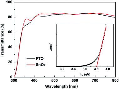 | ||
| Fig. 7 Transmission spectra of FTO substrates and with a 0.1 M SnO2 nanocrystalline film. The inserted curve reveals the diagram of (αhν)2 against hν calculated from Fig. 7. | ||
For planar Ag2S heterojunction solar cells, the morphologies of substrates also have an important influence on the device performance. A smooth interface is essential for achieving a higher FF for planar devices. We studied the interface between the absorber and the ETL. Fig. 8 shows atomic force microscopy (AFM) images of the SnO2 films coated from solutions of different SnO2 concentrations, 0.02, 0.1 and 0.5 M and bare FTO substrate. By increasing the concentration of SnCl2·2H2O in the solution, the films get thicker and smoother. The root-mean-square roughness (RMS) of the film made from a 0.1 M solution is only 0.769 nm which is as smooth as that of an ITO film. Films become rougher with increased concentration of SnO2 in the solution and the surface roughness of the film from a 0.5 M solution is almost identical to that of an ITO substrate. Compared with 0.5 M, 0.02 M cause an increase of RMS from 0.853 nm to 0.945 nm. Thicknesses of the SnO2 films from the 0.02 M and the 0.05 M solutions are too thin, it is not clear if those thin SnO2 films from the 0.02 M solutions can cover the entire FTO surface. Considering about the slightly lower FF of devices, we may contribute this phenomenon to the imperfect smooth morphology of SnO2 film.
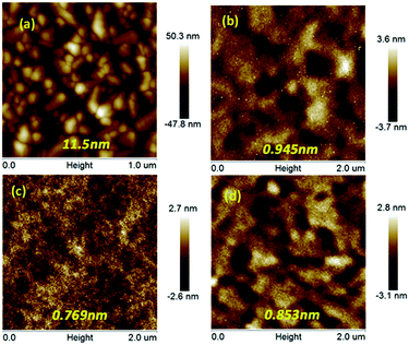 | ||
| Fig. 8 AFM images and the square average roughness (RMS) of (a) bare FTO, (b) 0.1 M SnO2 films on FTO, (c) 0.02 M SnO2 films on FTO and (d) 0.5 M SnO2 films on FTO. | ||
3.4. Study of novel SnO2 ETLs based Ag2S solar cells
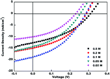
J–V characteristics of photovoltaic devices using SnO2 electron transport layers from the solutions of different SnO2 concentrations are depicted in Fig. 9 and detailed parameters are summarized in Table 2. The device using a 0.1 M SnO2 solution shows the best power conversion efficiency (PCE) of 2.1%, with open-circuit voltage (VOC) of 0.28 V, short-circuit current (JSC) of 19.3 mA cm−2, and fill factor (FF) of 40.4%, in order to check the reproducibility of the device, more than 10 devices using the 0.1 M SnO2 solution were examined with the same condition. The maximum and average PCE were 2.1% and 1.96%, respectively, which suggests the devices using the solution processed SnO2 can constantly show the excellent performance. On the other hand, the device using a 0.5 M SnO2 solution exhibits slightly lower PCE of 1.52% with JSC of 12.6 mA cm−2 and FF of 38.7%, which can be attributed to its high series resistance (Rs) of 14.8 Ω cm2 compared to an 10.8 Ω cm2 for the 0.1 M SnO2 solution.| SnO2 concentration (M) | VOC (V) | JSC (mA cm−2) | Rs (Ω cm2) | FF (%) | PCE (%) |
|---|---|---|---|---|---|
| a There are 12 samples for each device in this study. The errors of PCEs are ±0.1%. | |||||
| 0.50 | 0.31 | 12.6 | 14.8 | 38.7 | 1.52 |
| 0.20 | 0.29 | 14.9 | 12.3 | 38.6 | 1.76 |
| 0.10 | 0.28 | 19.3 | 10.8 | 40.4 | 2.10 |
| 0.05 | 0.25 | 14.3 | 13.7 | 38.1 | 1.37 |
| 0.02 | 0.23 | 10.2 | 16.3 | 38.4 | 0.90 |
Similar declined results were obtained with the device using a 0.02 M solution, PCE decreased compared to optimal SnO2 concentration. As mentioned above, the morphologies of substrates have an important influence on the device performance. Compared to the interface RMS value of 0.94 nm using 0.02 M solution, the interface of 0.1 M solution is smoother. This smooth surface was very helpful to reduce the recombination of light induced excitations at the interface of the absorber and electron conductor, which would be beneficial for achieving a higher FF for planar devices.
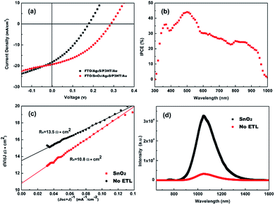
By carefully controlling the interfaces of the devices and the film thickness, we achieved best-performing solar cells based on SnO2 ETL efficiency of 2.10%, a VOC of 0.28 V, a JSC of 19.3 mA cm−2 and a FF of 40.4%, whereas the best performing solar cells without ETL show an efficiency of 1.10% with a VOC of 0.18 V, a JSC of 18.1 mA cm−2 and a FF of 33.5%. The corresponding J–V curves and parameters are presented in Fig. 10(a) and Table 3, we also make a comparison with the literature reported on metal-sulfide based solar cells in Table 3. We believe that our solution-processed SnO2 provides a superior electron transport for highly-efficient, easily-fabricated and low-cost solar cells based on Ag2S.
| Cell structure | VOC (V) | JSC (mA cm−2) | FF (%) | PCE (%) | References |
|---|---|---|---|---|---|
| FTO/Ag2S/P3HT/Au | 0.18 | 18.16 | 33.5 | 1.10 | |
| FTO/SnO2/Ag2S/P3HT/Au | 0.28 | 19.3 | 40.4 | 2.10 | |
| TCO/CdS/SnS/C/Ag | 0.27 | 6 | 44 | 0.7 | 35 |
| Mo/SnS/Zn(O,S)/ZnO/ITO | 0.26 | 24.9 | 44.4 | 2.9 | 36 |
| ITO/TiO2/CdS/Sb2S3:P3HT/PEDOT:PSS/Ag | 0.73 | 3.85 | 46 | 1.29 | 37 |
| Dense-TiO2/Sb2S3/P3HT/Au | 0.55 | 12.3 | 69.9 | 5.06 | 38 |
| FTO/Sb2Se3/CdS/ZnO/ZnO:Al/Au | 0.35 | 17.8 | 33.5 | 2.1 | 39 |
| FTO/SnO2/Sb2S3/P3HT/Au | 0.58 | 10.5 | 45.2 | 2.8 | 40 |
The prepared P3HT:Ag2S devices exhibited outstanding short-circuit current density around 19.3 mA cm−2. The basis for a high short circuit current of this type of solar cells is the photocurrent generation over a broad range of the solar spectrum, as is revealed by the IPCE spectrum in Fig. 10(b). Already at a wavelength of 800 nm, where Ag2S is the only absorbing material, the IPCE shows significant photocurrent generation.
As mentioned above, a strong contributing factor of VOC enhancement in SnO2 ETL based devices is conduction-band offset between Ag2S and its n-type ETLs material. As we know, the VOC is determined by the hole and electron electrochemical potential difference, or quasi-Fermi level separation in the material. This separation may be limited by bulk recombination, which reduces the concentration of free photoexcited carriers, or limited by the electrochemical potential of electrons in the n-type ETL. A small positive conduction band offsets (spike-like) can moderately improve the VOC by providing a barrier for electrons in the ETL from diffusing back into the low-lifetime bulk Ag2S and recombining with holes. From a theoretical point of view, a small conduction band offsets in the range of 0 eV to 0.4 eV is the optimal band alignment.
We also noticed an obvious enhancement of photocurrent for SnO2 devices. Except for the wider bandgap and a small positive conduction band offsets (spike-like), we also found other important characteristics for SnO2-based devices. To further clarify the photovoltaic characteristics, a model based on the single heterojunction solar cell is put forward to analyze the I–V property of the device, from which we can get the series resistance (Rs) according to the linear fit of the data.
4. Conclusion
In conclusion, we present a facile solution-based route towards nanostructured, hybrid absorber layers based on Ag2S. All of the material fabrication and device assembly processes were performed at low temperature and thus consumed negligible energy. The planar structure hybrid solar cell P3HT:Ag2S exhibits outstanding short circuit current density around 19 mA cm−2.Moreover, using a low-temperature solution-processed SnO2 as the ETL material, we most notably observed two characteristic improvements in the device performance: increased FF and VOC. The largest of which occurs at the solution concentration from a 0.1 M solution. The best-performing hybrid solar cell, using solution-processed SnO2 ETL, has achieved a PCE of 2.1% with a high VOC of 0.28 V, a high JSC of 19.3 mA cm−2, and a FF of 40.4%. However, device performance was limited by the Ag2S intrinsic bulk defects limited by the solvent thermal synthetic methods and suboptimal band gap. Further device configuration and processing optimization should boost the efficiency of Ag2S solar cell to a new level.
Acknowledgements
This work was supported by the by the National High Technology Research and Development Program (2015AA050601), the National Natural Science Foundation of China (61376013), the Natural Science Foundation of Jiangsu Province (BK20131186), the program of Suzhou Science & Technology Bureau (SYG201449), the Fundamental Research Funds for the Central Universities (20152020203).References
- W. Ke, G. Fang, Q. Liu, L. Xiong, P. Qin, H. Tao, J. Wang, H. Lei, B. Li, J. Wan, G. Yang and Y. Yan, J. Am. Chem. Soc., 2015, 137, 6730–6733 CrossRef CAS PubMed.
- J. T. Dufton, A. Walsh, P. M. Panchmatia, L. M. Peter, D. Colombara and M. S. Islam, Phys. Chem. Chem. Phys., 2012, 14, 7229–7233 RSC.
- K. Kim, L. Larina, J. H. Yun, K. H. Yoon, H. Kwon and B. T. Ahn, Phys. Chem. Chem. Phys., 2013, 15, 9239–9244 RSC.
- P. Loper, S. J. Moon, S. M. de Nicolas, B. Niesen, M. Ledinsky, S. Nicolay, J. Bailat, J. H. Yum, S. De Wolf and C. Ballif, Phys. Chem. Chem. Phys., 2015, 17, 1619–1629 RSC.
- H. Lei, G. Fang, F. Cheng, W. Ke, P. Qin, Z. Song, Q. Zheng, X. Fan, H. Huang and X. Zhao, Sol. Energy Mater. Sol. Cells, 2014, 128, 77–84 CrossRef CAS.
- X. Tu, F. Wang, C. Li, Z. A. Tan and Y. Li, J. Phys. Chem. C, 2014, 118, 9309–9317 CAS.
- Z. Zhai, X. Huang, M. Xu, J. Yuan, J. Peng and W. Ma, Adv. Energy Mater., 2013, 3, 1614–1622 CrossRef CAS.
- F. Gao, Q. Lu and D. Zhao, Nano Lett., 2003, 3, 85–88 CrossRef CAS.
- S. Hull, D. Keen, D. Sivia, P. Madden and M. Wilson, J. Phys.: Condens. Matter, 2002, 14, L9 CrossRef CAS.
- B. R. McNamara, P. E. Nulsen, M. W. Wise, D. A. Rafferty, C. Carilli, C. L. Sarazin and E. L. Blanton, Nature, 2005, 433, 45–47 CrossRef CAS PubMed.
- X. Wen, S. Wang, Y. Xie, X. Y. Li and S. Yang, J. Phys. Chem. B, 2005, 109, 10100–10106 CrossRef CAS PubMed.
- M. A. Hossain, J. R. Jennings, Z. Y. Koh and Q. Wang, ACS Nano, 2011, 5, 3172–3181 CrossRef CAS PubMed.
- P. Meduri, C. Pendyala, V. Kumar, G. U. Sumanasekera and M. K. Sunkara, Nano Lett., 2009, 9, 612–616 CrossRef CAS PubMed.
- H. J. Snaith and C. Ducati, Nano Lett., 2010, 10, 1259–1265 CrossRef CAS PubMed.
- S. Trost, K. Zilberberg, A. Behrendt and T. Riedl, J. Mater. Chem., 2012, 22, 16224 RSC.
- Y. Li, G. Chen, C. Zhou and J. Sun, Chem. Commun., 2009, 2020–2022 RSC.
- Q. Lu, F. Gao and D. Zhao, Angew. Chem., 2002, 114, 2012–2014 CrossRef.
- D. Wang, C. Hao, W. Zheng, Q. Peng, T. Wang, Z. Liao, D. Yu and Y. Li, Adv. Mater., 2008, 20, 2628–2632 CrossRef CAS.
- S. Mandal, A. Gole, N. Lala, R. Gonnade, V. Ganvir and M. Sastry, Langmuir, 2001, 17, 6262–6268 CrossRef CAS.
- Z. Zhong, A. S. Subramanian, J. Highfield, K. Carpenter and A. Gedanken, Chemistry, 2005, 11, 1473–1478 CrossRef CAS PubMed.
- J. Xiao, Y. Xie, R. Tang and W. Luo, J. Mater. Chem., 2002, 12, 1148–1151 RSC.
- C. Xu, Z. Zhang and Q. Ye, Mater. Lett., 2004, 58, 1671–1676 CrossRef CAS.
- C. Wagner, W. Riggs, L. Davis, J. Moulder and G. Muilenberg, Handbook of X-ray Photoelectron Spectroscopy, 1979, pp. 74–80 Search PubMed.
- J. Xiang, H. Cao, Q. Wu, S. Zhang, X. Zhang and A. A. Watt, J. Phys. Chem. C, 2008, 112, 3580–3584 CAS.
- A. Grosvenor, B. Kobe, M. Biesinger and N. McIntyre, Surf. Interface Anal., 2004, 36, 1564–1574 CrossRef CAS.
- B. Zhang, X. Ye, W. Dai, W. Hou and Y. Xie, Chemistry, 2006, 12, 2337–2342 CrossRef CAS PubMed.
- K. Ramasamy, H. Sims, W. H. Butler and A. Gupta, Selective Nanocrystal Synthesis and Calculated Electronic Structure of All Four Phases of Copper–Antimony–Sulfide, Chem. Mater., 2014, 26, 2891–2899 CrossRef CAS.
- R. Vogel, P. Hoyer and H. Weller, J. Phys. Chem., 1994, 98, 3183–3188 CrossRef CAS.
- M. Luo, M. Leng, X. Liu, J. Chen, C. Chen, S. Qin and J. Tang, Thermal evaporation and characterization of superstrate CdS/Sb2Se3 solar cells, Appl. Phys. Lett., 2014, 104, 173904 CrossRef.
- R. Yang, D. Wang, L. Wan and D. Wang, RSC Adv., 2014, 4, 22162–22171 RSC.
- B. Bob, T.-B. Song, C.-C. Chen, Z. Xu and Y. Yang, Chem. Mater., 2013, 25, 4725–4730 CrossRef CAS.
- M. Kwoka, L. Ottaviano, M. Passacantando, S. Santucci, G. Czempik and J. Szuber, Thin Solid Films, 2005, 490, 36–42 CrossRef CAS.
- J. Wang, M. Qin, H. Tao, W. Ke, Z. Chen, J. Wan, P. Qin, L. Xiong, H. Lei, H. Yu and G. Fang, Appl. Phys. Lett., 2015, 106, 121104 CrossRef.
- S. Gubbala, V. Chakrapani, V. Kumar and M. K. Sunkara, Adv. Funct. Mater., 2008, 18, 2411–2418 CrossRef CAS.
- D. Avellaneda, B. Krishnan, T. K. Das Roy, G. A. Castillo and S. Shaji, J. Mater. Sci.: Mater. Electron., 2013, 110, 667–672 CAS.
- H. H. Park, R. Heasley, L. Sun, V. Steinmann, R. Jaramillo, K. Hartman, R. Chakraborty, P. Sinsermsuksakul, D. Chua, T. Buonassisi and R. G. Gordon, Prog. Photovoltaics Res. Appl., 2015, 23, 901–908 CrossRef CAS.
- N. Bansal, F. T. F. O'Mahony, T. Lutz and S. A. Haque, Adv. Energy Mater., 2013, 3, 986–990 CrossRef CAS.
- J. A. Chang, J. H. Rhee, S. H. Im, Y. H. Lee, H. J. Kim, S. I. Seok, M. K. Nazeeruddin and M. Gratzel, Nano Lett., 2010, 10, 2609–2612 CrossRef CAS PubMed.
- X. Liu, J. Chen, M. Luo, M. Leng, Z. Xia, Y. Zhou, S. Qin, D. J. Xue, L. Lv, H. Huang, D. Niu and J. Tang, ACS Appl. Mater. Interfaces, 2014, 6, 10687–10695 CAS.
- L. Hongwei, et al., Efficient planar Sb2S3 solar cells using a low-temperature solution-processed tin oxide electron conductor, Phys. Chem. Chem. Phys., 2016 10.1039/c6cp02072k.
| This journal is © The Royal Society of Chemistry 2016 |

