O. V. Parasyuka,
V. V. Pavlyukbc,
O. Y. Khyzhund,
V. R. Kozera,
G. L. Myronchuke,
V. P. Sachanyuka,
G. S. Dmytrivb,
A. Krymusef,
I. V. Kitykf,
A. M. El-Naggargh,
A. A. Albassamh and
M. Piasecki*i
aDepartment of Inorganic and Physical Chemistry, Lesya Ukrainka Eastern European National University, 13 Voli Ave., Lutsk 43025, Ukraine
bDepartment of Inorganic Chemistry, Ivan Franko National University of Lviv, 6 Kyryla and Mefodiya St., 79005 Lviv, Ukraine
cInstitute of Chemistry, Environment Protection and Biotechnology, Jan Dlugosz University, al. Armii Krajowej 13/15, 42-200 Czestochowa, Poland
dFrantsevych Institute for Problems of Materials Science, National Academy of Sciences of Ukraine, 3 Krzhyzhanivsky St., 03142 Kyiv, Ukraine
eDepartment of Solid State Physics, Lesya Ukrainka Eastern European National University, 13 Voli Ave., Lutsk 43025, Ukraine
fFaculty of Electrical Engineering, Czestochowa University Technology, Armii Krajowej 17, Czestochowa, Poland
gPhysics Department, Faculty of Science, Ain Shams University, Abassia, Cairo 11566, Egypt
hResearch Chair of Exploitation of Renewable Energy Applications in Saudi Arabia, Physics & Astronomy Dept., College of Science, King Saud University, P. O. Box 2455, Riyadh 11451, Saudi Arabia
iInstitute of Physics, J. Dlugosz Academy, Armii Krajowej 13/15, PL-42-201, Czestochowa, Poland. E-mail: m.piasecki@ajd.czest.pl
First published on 7th September 2016
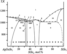
Phase diagrams of the AgGaSe2–SiSe2 system were explored by differential thermal analysis (DTA) and X-ray diffraction (XRD) analysis methods for the first time. It was demonstrated that the investigated system forms quaternary compounds of compositions Ag2Ga2SiSe6 and AgGaSiSe4. Ag2Ga2SiSe6 melts at 1042 K and exists in two polymorphous modifications. The crystal structure of the low-temperature modification was determined by the single crystal method (space group I2d (122) and lattice parameters a = 5.9021(1) Å, b = 5.9021(1) Å, and c = 10.4112(10) Å). Additional details (CIF file) regarding the crystal structure investigations are available at the Fachinformationszentrum Karlsruhe. The band gap (Eg) of the Ag2Ga2SiSe6 system was estimated from the fundamental absorption edge and we showed that it decreases with increasing temperature (100–300 K) from 2.13 eV to 1.97 eV. The compound is photosensitive and its spectral dependence on the photoconductivity has two maxima: at λmax1 = 640 nm and λmax2 = 900 nm. For the pristine Ag2Ga2SiSe6 crystal surface, X-ray photoelectron core-level and valence-band spectra were obtained. The X-ray photoelectron valence-band spectrum of Ag2Ga2SiSe6 was compared on a common energy scale with the X-ray emission Se Kβ2 and Ga Kβ2 bands, representing peculiarities of the energy distribution of the Se 4p and Ga 4p states, respectively. The comparison revealed that the principal contributions of the valence Se p and Ga p states occur in the upper and central parts of the valence band, respectively, with significant contributions to other valence band regions. The illumination by the bicolour coherent pulses of the Er:glass nanosecond lasers at different angles led to the formation of the gratings, which are sensitive to the irradiation time.
The technology of the single crystal production of the quaternary phase is much simpler as well. They were grown by the Bridgman–Stockbarger method1,4,5,7,9–12 or horizontal gradient freeze technique in transparent furnaces.13 In addition to promising non-linear optical susceptibilities, the quaternary phase is also a promising piezoelectric14 and acousto-optical material for the mid-IR spectral range.15 The wide, homogeneity region of AGGSe permits a certain range of tuning of their parameters, and the peculiarities of the crystal structure lead to the formation of solid solutions by the substitution of any of the components of the compound.16–18
The latter feature makes advisable the study of a similar system with silicon diselenide instead of germanium diselenide (no intermediate phase was found with SnSe2 (ref. 19)). The existence of compounds in the AgGaSe2–SiSe2 system was indicated earlier. Goodchild et al.20 reported the formation of the AgGaSiSe4 compound as one of the representatives of the I-III-IV-VI family. Quite recently, Zhang et al.21 obtained AgGaSiSe4 by the solid state phase growth of equimolar amounts of AGSe and SiSe2 at 970 K during 24 h (the procedure was repeated with intermediate powdering). The crystal structure determined following the single crystal method is orthorhombic (space group Aea2) with rather large unit cell parameters a = 62.905 Å, b = 7.115 Å, c = 12.376 Å and Z = 32. The compound melts congruently at 1032 K and has the energy band gap equal to 2.63(2) eV, following the reflectance spectra. The growth of Ag3Ga3SiSe8, also melting congruently at 1057 K, was reported in ref. 22. This compound is isostructural with AGSe (space group I2d, a = 0.59041 nm, c = 1.0499 nm, Z = 1) and has the band gap equal to about 2.30 eV. It was additionally reported that its non-linear optical properties are similar to those of AGSe.
Here, we present the results of the investigation of the phase diagram of the AgGaSe2–SiSe2 system for the first time, its crystal and electronic structure and some properties of the Ag2Ga2SiSe6 compound.
All the initial compounds and intermediate alloys were studied by differential thermal analysis (DTA) using the Paulik–Paulik–Erdey derivatograph (Pt/Pt–Rh thermocouple). The heating rate was 10 K min−1. XRPD investigation was performed by DRON 4–13 diffractometer using CuKα-radiation.
Single crystal data were collected at ambient temperature, using a four-circle diffractometer (Xcalibur Oxford Diffraction diffractometer) with CCD detector (graphite monochromatized Mo-Kα radiation, λ = 0.071073 nm). Scans were taken in the ω mode, the empirical absorption corrections were made by CrystalisRed.23 The crystal structures of the quaternary compounds investigated in the present work were successfully solved by direct methods and refined using SHELX–97 package programs.24
In order to elucidate the peculiarities of the electronic structure and chemical bonding in the synthesized Ag2Ga2SiSe6 specimen, we used the X-ray photoelectron spectroscopy (XPS) in order to perform measurements of the XPS valence-band and core-level spectra. The measurements were made by employing the UHV-Analysis-System designed and assembled by SPECS Surface Nano Analysis Company (Germany). The UHV-Analysis-System is equipped with a PHOIBOS 150 hemispherical analyzer. The XPS spectra were collected using the Ag2Ga2SiSe6 crystal sample. The XPS measurements were made in an ion-pumped chamber having a base pressure less than 6 × 10⁻¹⁰ mbar. The XPS spectra of the Ag2Ga2SiSe6 sample were excited by a Mg Kα source of X-ray radiation (E = 1253.6 eV) and were recorded at a constant pass energy of 35 eV. The spectrometer energy scale was calibrated as described in ref. 25. The C 1s line (284.6 eV) of adventitious carbon was used as a reference to account for the charging effects, as it is suggested for relative quaternary Ag- and/or Ga-bearing chalcogenides.26–28 Since in the Ag- and/or Ga-bearing ternary and quaternary tetra and sextasulfides (selenides) their electronic structures are determined by significant contributions of the valence S (Se) p and Ga p states throughout the whole valence band region (see ref. 27–31), we have also measured X-ray emission Se(Ga) Kβ2 bands (K → MII,III transition) representing the energy distribution of the Se(Ga) 4p states and compared them on a common energy scale with the XPS valence-band spectrum of Ag2Ga2SiSe6. The fluorescent X-ray emission Se(Ga) Kβ2 bands were recorded using a Johann-type DRS-2M spectrograph equipped with an X-ray BHV-7 tube (gold anode) and a quartz crystal with the (0001) reflecting plane, following the technique described in detail in ref. 32 and 33. The spectrograph energy resolution was determined to be about 0.3 eV in the energy regions corresponding to the position of the measured X-ray emission Se(Ga) Kβ2 bands.
The polymorphous transition of Ag2Ga2SiSe6 takes place in the subsolidus region in the temperature range of 1009–1021 K, which indicates a certain homogeneity region for the quaternary phase at this temperature. The homogeneity region at the annealing temperature does not exceed 2 mol%. The structure of the low-temperature modification of the quaternary compound is tetragonal (see next chapter). We could not resolve the structure of HT-Ag2Ga2SiSe6, mainly due to the narrow temperature range of its existence. The interaction of HT-Ag2Ga2SiSe6 and AgGaSiSe4 is eutectic, with the invariant point coordinates of 37 mol% SiSe2 and 1027 K. AgGaSiSe4 and SiSe2 also form a eutectic point at 63 mol% SiSe2 and 1010 K. We tried to synthesize a high temperature modification of Ag2Ga2SiSe6, however, it was not possible, due to the narrow temperature range of its existence in a non-congruent type of compound formation. We attempted to harden the alloy during 100 hours at 1030 K and additionally, we tried to harden it during 100 hours at temperature 1030 K and liquidus higher than 50 K. Similarly, in the sulfur containing compounds,34 the temperature range for high temperature modification is higher. However, in this case, we obtained a diffractogram containing a mixture of diffraction maxima originating from both modifications. The solid solubility in AgGaSe2 was determined by the variation of the lattice periods at 670 K (Fig. 2), and reached 9 mol% SiSe2.
The AgGaSiSe4 has an open melting maximum at 1047 K, which agrees well with ref. 21. A flat melting maximum of AgGaSiSe4 indicates partial dissociation of this compound in the melt. The homogeneity region of AgGaSiSe4 is quite wide at the eutectic temperature of (∼46–58 mol% SiSe2), but is narrowed considerably at lower temperatures.
Therefore, during the investigation of the AgGaSe2–SiSe2 phase diagram, we ascertained the composition of the known compound Ag3Ga3SiSe8 (25 mol% SiSe2). According to our results, it is described by the formula Ag2Ga2SiSe6 (33.3 mol% SiSe2). Diffraction patterns for the alloys of the system in the 0–50 mol% SiSe2 region are shown in Fig. 3. Three sets of diffraction reflections are observed in this range. Diffraction pattern (1) corresponds to the AgGaSe2 compound, which crystallizes in the tetragonal chalcopyrite structure (SG I2d), the pattern (6) corresponds to the Ag2Ga2SiSe6 compound, which crystallizes in the same space group, and the pattern (8) corresponds to AgGaSiSe4. Despite having the same space group, their solid solubilities are rather modest (0–8 mol% SiSe2). Although the diffraction patterns of the compounds are similar, the diffraction patterns of the intermediate alloys clearly exhibit the superposition of the reflections of both phases, with the gradual growth of the intensity of the reflections of the quaternary phases with the increase of the SiSe2 content. It should also be emphasized that the 2-2-1-6 compounds are often found in the systems of this type. The first representative was Ag2In2GeSe6 (SG Cc).35 Later, they were found in other silver-containing systems, Ag2In2Si(Ge)S6 (ref. 36) and Ag2In2SiSe6 (ref. 37) (all SG Cc), as well as copper- (Cu2In2SiS6 (SG Cc)38), lithium- (Li2In2MX6 (M = Si,Ge; X = S, Se) (SG Cc)38,39) and sodium-containing systems (Na2M2M′S6 (M = Ga, In, M′ = Si, Ge, Sn) (SG Fdd2 or Cc)40,41).
![]() | ||
Fig. 3 Diffraction patterns of the alloys of the AgGaSе2–SiSе2 system quenched from 670 K (all in mol% SiSe2): (1) 0, (2) 10, (3) 15, (4) 25, (5) 30, (6) 33.3, (7) 40, (8) 50. |
Crystal data | |
Ag2.85Ga2.78Si1.22Se8 (or Ag2.13Ga2.08Si0.92Se6) | V = 362.67(4) Å3 |
Mr = 1167.20 | Z = 1 |
Tetragonal, I![]() |
F(000) = 509 |
a = 5.9021(1) Å | Dx = 5.344 g cm−3 |
b = 5.9021(1) Å | Mo Kα radiation, λ = 0.71073 Å |
c = 10.4112(10) Å | μ = 29.00 mm−1 |
α = 90° | T = 293 K |
β = 90° | 0.06 × 0.05 × 0.01 mm |
γ = 90° | |
![]() |
|
Data collection | |
Radiation source: fine-focus sealed tube | Rint = 0.083 |
Graphite | θmax = 29.3°, θmin = 4.0° |
3035 measured reflections | h = −8 → 7 |
242 independent reflections | k = −8 → 8 |
217 reflections with I > 2σ(I) | l = −13 → 14 |
![]() |
|
Refinement | |
Refinement on F2 | Secondary atom site location: difference Fourier map |
R[F2 > 2σ(F2)] = 0.026 | w = 1/[σ2(F02) + (0.018P)2 + 0.438P] where P = (F02 + 2Fc2)/3 |
wR(F2) = 0.061 | (Δ/σ)max < 0.001 |
S = 1.13 | Δ>max = 0.83 e Å−3 |
242 reflections | Δ>min = −0.76 e Å−3 |
13 parameters | Absolute structure: Flack H D (1983), Acta cryst. A39, 876–881 |
0 restraints | Flack parameter: 0.04 (3) |
The obtained single crystal data show that the Ag2Ga2SiSe6 compound crystallizes with the tetragonal space group I2d as a disordered derivative structure from the CuFeS2 type. The refined fractional atomic coordinates and displacement parameters are given in Table 2. The projections of the unit cell and coordination polyhedra of the atoms are shown in Fig. 4. The inter-atomic distances are listed in Table 3. All the atoms are enclosed in tetrahedrons. The packing architecture of tetrahedrons in the unit cell is shown in Fig. 5.
Atom | Site | x | y | z | Uiso*/Ueq | Occ |
---|---|---|---|---|---|---|
Se1 | 8d | 0.22293 (10) | 0.2500 | 0.1250 | 0.0294 (3) | 1.000 |
Ag2 | 4b | 0.0000 | 0.0000 | 0.5000 | 0.0329 (4) | 0.713 (3) |
Ga3 | 4a | 0.0000 | 0.0000 | 0.0000 | 0.0158 (4) | 0.695 (4) |
Si3 | 4a | 0.0000 | 0.0000 | 0.0000 | 0.0158 (4) | 0.305(4) |
![]() |
||||||
U11 | U22 | U33 | U12 | U13 | U23 | |
Se1 | 0.0133 (3) | 0.0266 (4) | 0.0483 (5) | 0.000 | 0.000 | -0.0182 (3) |
Ag2 | 0.0313 (5) | 0.0313 (5) | 0.0360 (6) | 0.000 | 0.000 | 0.000 |
Ga3/Si3 | 0.0142 (5) | 0.0142 (5) | 0.0189 (6) | 0.000 | 0.000 | 0.000 |
Se1—Ga3 | 2.3669 (3) | Ag2–Se1v | 2.5583 (4) |
Se1–Si3i | 2.3669 (3) | Ag2–Se1vi | 2.5583 (4) |
Se1—Ga3i | 2.3669 (3) | Ag2–Se1vii | 2.5583 (4) |
Se1–Ag2ii | 2.5583 (4) | Ga3—Se1viii | 2.3669 (3) |
Se1–Ag2iii | 2.5583 (4) | Ga3—Se1ix | 2.3669 (3) |
Ag2–Se1iv | 2.5583 (4) | Ga3—Se1x | 2.3669 (3) |
In order to avoid statistical mixture of Ga/Si atoms, the structure was transformed into the tetragonal space group I (a = 5.9021 Å, b = 5.9021 Å, c = 10.4112 Å; Se in 8g: x = 0.2247, y = 1/4, z = 1/8; Ag1 in 2b: x = 0, y = 0, z = 1/2; Ag2 in 2d: x = 0, y = 1/2, z = 3/4; Ga in 2a: x = 0, y = 0, z = 0; Si in 2c: x = 0, y = 1/2, z = 1/4) in which gallium and silicon atoms occupy separate sites, 2a and 2c, respectively.
However, attempts to refine the Ag2Ga2SiSe6 structure in the possible I space group were unsuccessful. The better results were obtained for the tetragonal disordered structure model in the I
2d space group. Further details of the AgGaSiSe4 crystal structure investigations (also CIF file) can be obtained from the Fachinformationszentrum (FIZ) Karlsruhe.†
Data from measurements of the binding energies for constituent element core-level electrons of the Ag2Ga2SiSe6 crystal surface are listed in Table 4, whereas Fig. 5 displays the principal core-level spectra of the atoms constituting the quaternary Ag2Ga2SiSe6 compound. These results indicate that the binding energies of the Ag 3d5/2, Ge 2p3/2 and Se 3p3/2 (3d) core-level electrons correspond to Ag+, Ga3+ and Se2−, respectively.42 The effective charge state of the Si atoms in Ag2Ga2SiSe6 is difficult to evaluate because the XPS Si 2p line is superimposed by the Ga 3p core-level spectrum, while the Si 2s line – by the Se 3p terms (see Fig. 7). Following Fig. 8, the XPS valence-band spectrum of the Ag2Ga2SiSe6 crystal reveals two fine-structure peculiarities, namely A and B. In order to clarify the peculiarities of the occupation of the valence band by the Se 4p and Ga 4p states in the Ag2Ga2SiSe6 compound, we have made the comparison of its X-ray emission Se Kβ2 and Ga Kβ2 bands and the XPS valence-band spectrum, using a common energy scale. The result of such a comparison is plotted in Fig. 9. It is worth mentioning that the zero energy of the X-ray emission Se Kβ2 and Ga Kβ2 bands and the XPS valence-band spectrum shown in Fig. 9, correspond to the position of the Fermi level of the PHOIBOS 150 hemispherical energy analyzer of the UHV-Analysis-System. Following Fig. 9, the energy position of the fine-structure peculiarity A of the XPS valence-band spectrum of Ag2Ga2SiSe6 corresponds to the spectral position of the maximum of the X-ray emission Se Kβ2 band, while the maximum of the X-ray emission Ga Kβ2 band is positioned in the central portion of the XPS valence band spectrum. Furthermore, the above experimental results reveal that the Se 4p and Ga 4p states contribute significantly in other parts of the valence band region of Ag2Ga2SiSe6.
Core-level line/valence band spectrum | Binding energy |
---|---|
a Uncertainty of the measurements is ±0.1 eV. | |
Valence band region (features A and B) | 3.5, 5.9 |
Ga 3d | 20.2 |
Se 3d | 54.6 |
Si 2p | 104.7 |
Se 3p3/2 | 160.9 |
Se 3p1/2 | 166.1 |
Ag 3d5/2 | 367.9 |
Ag 3d3/2 | 374.0 |
Ga 3p3/2 | 1117.8 |
![]() | ||
Fig. 7 Detailed XPS core-level spectra of the Ag2Ga2SiSe6 crystal: (a) Ga 3p3/2, (b) Ag 3d, (c) Se 3p and Si 2s, (d) Si 2p and Ga 3p, and (e) Se 3d. |
![]() | ||
Fig. 8 Detailed XPS valence-band spectrum (including upper Ga 3d core-level) of the of the Ag2Ga2SiSe6 crystal. |
![]() | ||
Fig. 9 Comparison, on a common energy scale, of the XPS valence-band spectrum and the X-ray emission Se Kβ2 and Ga Kβ2 bands of the Ag2Ga2SiSe6 crystal. |
Unfortunately, the available facilities do not allow the measurement of the energy distribution of the valence Si (s, p) and Ag (d) states, which are expected to be the other significant contributors to the Ag2Ga2SiSe6 valence-band region.
The temperature coefficient of the band gap variation (Eg (T) = Eg77 − β(T − 77)) was calculated as β = 7×10⁻³ eV K−1. The obtained value is close to that of the majority of disordered chalcogenide semiconductors.43
The Ag2Ga2SiSe6 crystals are photosensitive semiconductors, with the conductivity multiple of 1.4 (300 K) upon illumination of 100 lux white light. The spectral distribution of the photoconductivity (SDP) of the studied compound is shown in Fig. 12. The low photosensitivity of the crystals is likely caused by the high concentration of rapid recombination centers that are usually related to the intrinsic defects of the crystal lattice. This is confirmed by the large half-width (∼200 nm) of the peak of the intrinsic photoconductivity. A characteristic feature of SDP is the presence of two maxima: I (λmax1 = 640 nm) and II (λmax2 = 900 nm). The first SDP maximum (λmax1) of all investigated samples lies in the region of the edge of the fundamental absorption band, and is unambiguously caused by the intrinsic photoconductivity of the semiconductor. No substantial changes were observed in SDP at 77 K (compared to ambient temperature), except a moderate shift of the intrinsic photoconductivity maximum to the higher energy region, due to an increased Eg of the compound at lower temperature.
After 1 min of the treatment, there occurred some interferograms, as shown in Fig. 13. The gratings occurred in a very narrow angle range, within 20–21°, with respect to the sample surface. Additionally, the pictures are clearly seen at some fixed ratios of intensities between the fundamental and the doubled frequency beam, varying between 4:
1 up to 6
:
1. The sketches are presented for the power densities of the photoinducing beams, about 0.5 GW cm−2. After 2–3 min, the process was saturated with the higher space frequencies (see Fig. 13). The origin of the effect is caused by the coexistence of the third and second order susceptibility tensors. The gratings thus formed were relaxed after several seconds, without any irreversible changes.
![]() | ||
Fig. 13 General sketch of the grating plots at two different times of illuminations at power density of 400 MW cm−2: (a) at time of about 1 min; (b) at time of illumination of 3 min. |
For the formation of such gratings, the occurrence of photoconductivity carriers that will favor the occurrence of the gratings is very crucial.
The proper second order optical effects, i.e., second harmonic generation, are relatively weak (about 0.5 pm V−1 at 1064 nm). However, additional bicolour optical treatment leads to the formation of the stable gratings. The latter is determined by the intrinsic defect trapping states situated within the energy gap.
Based on the above, these crystals could be promising materials for dynamic holographic image recording, and they may be comparable to other chalcogenide crystals.45
Comparison of the nonlinear optical properties of similar compounds, AgGaSe2, Ag3SiSe8 and GaSe–AgGaSe2,46–48 has shown that the Ga(Si)–Se4 structural clusters should play the principal role. Following these reasons and considering the crystallochemistry presented in Fig. 4 and 5, we performed B3LYP DFT quantum chemical calculations for the principal structural fragments by a method described in ref. 18. We discovered that the ground state dipole moment for the Si–Se4 cluster is about 9.8 D, and 7.8 D for the Ga–Se4 cluster, which is almost half order higher with respect to other clusters.
To understand the origin of the optical and photoinduced effects observed, we performed B3LYP DFT quantum chemical calculations for the principal structural fragments (clusters) by a method described in the literature18. We discovered that the dipole moments of the Si–Se4 cluster and the Ga–Se4 cluster are equal to about 9.8 D and 7.8 D, respectively, which is almost half order higher with respect to other clusters, including those with silver. Therefore, all further designs of such kinds of materials with improved optical features should be concentrated on optimization of the Ga(Si)–Se4 clusters. Additionally, these clusters possess higher polarization, which may have potential for use in optical treatment.
The title crystals were explored with respect to the formation of all-optical gratings and the single crystals were illuminated by two coherent beams originating from pulsed Er:glass lasers. The gratings occurred in a very narrow angle range, within 20–21°, with respect to the sample surface. Additionally, the pictures are clearly seen at some fixed ratios of intensities between the fundamental and the doubled frequency beam, varying from 4:
1 up to 6
:
1.
Footnote |
† Details of the AgGaSiSe4 crystal structure investigations (including the CIF file) can be obtained from the Fachinformationszentrum (FIZ) Karlsruhe, 76344 Eggenstein-Leopoldshafen, Germany (Fax: +(49) 7247- 808-666; e-mail: crysdata@fiz-karlsruhe.de), on quoting the appropriate CSD number: 431487. |
This journal is © The Royal Society of Chemistry 2016 |