
3C–SiC on glass: an ideal platform for temperature sensors under visible light illumination†
Abu Riduan Md Foisal *a,
Hoang-Phuong Phana,
Takahiro Kozekib,
Toan Dinha,
Khoa Nguyen Tuana,
Afzaal Qamara,
Mirko Lobinoac,
Takahiro Namazud and
Dzung Viet Daoae
*a,
Hoang-Phuong Phana,
Takahiro Kozekib,
Toan Dinha,
Khoa Nguyen Tuana,
Afzaal Qamara,
Mirko Lobinoac,
Takahiro Namazud and
Dzung Viet Daoae
aQueensland Micro-Nanotechnology Centre, Griffith University, Queensland, Australia. E-mail: ar.mdfoisal@griffithuni.edu.au
bDepartment of Mechanical Engineering, University of Hyogo, Hyogo, Japan
cCentre for Quantum Dynamics, Griffith University, Queensland, Australia
dDepartment of Mechanical Engineering, Aichi Institute of Technology, Toyota, Japan
eSchool of Engineering, Griffith University, Queensland, Australia
First published on 1st September 2016
Abstract
This letter reports on cubic silicon carbide (3C–SiC) transferred on a glass substrate as an ideal platform for thermoresistive sensors which can be used for in situ temperature measurement during optical analysis. The transfer of SiC onto an insulating substrate prevents current leakage through the SiC/Si junction, which is significantly influenced by visible light. Experimental data shows that the 3C–SiC on glass based sensor possesses a large temperature coefficient of resistance (TCR) of up to −7508 ppm K−1, which is about 10 times larger than that of highly doped Si. Moreover, the 3C–SiC based temperature sensor also outperforms low doped Si in terms of stability against visible light. These results indicate that 3C–SiC on glass could be a good thermoresistive sensor to measure the temperature of cells during optical investigations.
Accurate and continuous measurements of temperature are highly critical for monitoring the in situ conditions of chemical reactions and bio-mechanisms in cell culture (e.g., focal adhesion, morphogenesis, protein folding, and so on).1,2 The keys to achieve this are bio-compatibility, high thermosensitivity, fast response, etc. To date, silicon has been widely used to develop temperature sensors for cell monitoring, owing to its mature fabrication technology.3–5
However, in biochemical environments, silicon (Si) based sensors suffer from various difficulties, such as drifting potentials, chemical instability, and fouling encapsulation.6–9 These sensors also are not suitable for the optical analysis or in situ condition monitoring of cell culture under the microscope due to the opaqueness of Si at visible wavelengths. As a result, to measure the mechanical properties of a cell using a Si piezoresistive cantilever, a light compensation circuit is usually required.10 In addition, visible light would have a significant impact on the accurate measurement of cell temperature. Therefore, to investigate the mechanical properties and temperature of cells in an optical microscopy environment, sensors which are insensitive to visible wavelengths are desirable.
Compared to Si, silicon carbide (SiC) is a versatile material for bio-applications due to its superior mechanical and electrical properties, as well as chemical inertness.11–18 To date, there have been a large number of studies investigating and considering the development of SiC based biocompatible devices. For instance, Kalnins et al. utilized SiC as a protective layer for stents which can reduce early and late coronary events.19 SiC was also used as a ceramic coating material for titanium based total hip replacement implants.20 Godignon et al. reported that bulk SiC micro-needles can outperform Si for graft monitoring.21 However, the potential of using SiC for highly sensitive temperature sensors in an optical environment has not been demonstrated.
In this work, we demonstrate a highly sensitive temperature sensor using 3C–SiC transferred onto a glass substrate, as the glass substrate possesses excellent stability in optical environments. Experimental data showed that SiC on a glass substrate was insensitive to visible wavelengths (400–700 nm), thanks to the large band gap of SiC. In addition, SiC on glass also showed a large TCR of 7508 ppm K−1 which is 10 times larger than that of highly doped Si. All these properties along with the bio-compatibility of SiC make it an excellent candidate for bio-thermal sensing under illuminative environments.
Single crystalline p-type 3C–SiC was epitaxially grown on p-type Si(100) substrate by using hot wall Low Pressure Chemical Vapor Deposition (LPCVD) reactor at 1000 °C.22 The alternating supply epitaxy (ASE) approach was used to achieve single crystalline SiC film deposition with silane (SiH4) and propylene (C3H6) as precursors. Trimethylaluminium was used as a p-type dopant for in situ doping.
The full range (2θ–ω) of the X-ray diffraction (XRD) measurement indicated that 3C–SiC is epitaxially grown on the Si(100) substrate and the Transmission Electron Microscope (TEM) image depicts the good crystalline quality of the grown 3C–SiC film (ESI†). Using the Hall measurement, the carrier concentration of the 3C–SiC and Si substrate was found to be approximately 5 × 1018 cm−3 and 5 × 1014 cm−3, respectively. As we reported previously, under dark conditions, the leakage current through the 3C–SiC and Si junction was only about 0.05% of the applied current due to the large valence band discontinuity between 3C–SiC (Ev = 6.9 eV) and Si (Ev = 5.2 eV).23,24 However, the resistance of 3C–SiC/Si significantly decreased with increasing light intensity (approximately 27% at an intensity of 2.0 mW cm−2 and a wavelength of 488 nm), as shown in Fig. 1. This variation is attributed to either the absorption of light in the SiC layer or a change in the leakage current through the SiC/Si junction. To elucidate this phenomenon, we transferred the SiC onto an insulating substrate.
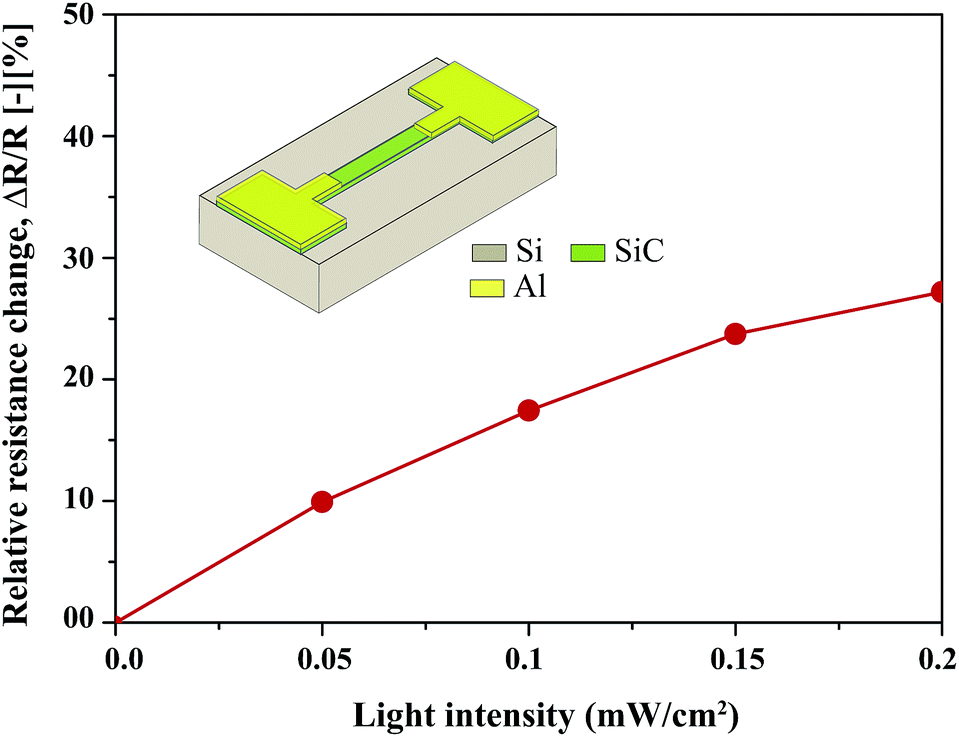 | ||
| Fig. 1 The variation in resistance of p-3C–SiC on the Si substrate under light illumination (inset shows a sketch of the 3C–SiC resistor on the Si substrate). | ||
I-shaped 3C–SiC resistors (inset of Fig. 1) were formed on Si using photolithography and inductively coupled plasma etching (ESI†). Xenon difluoride (XeF2) etching was employed to release the SiC from the Si substrate,25 Fig. 2(a). As shown in Fig. 2(b), the resistors were then detached from Si by the FIB technique. After that, using a microprobe, the SiC was transferred to a glass substrate, Fig. 2(c). A tungsten layer was then deposited to fix the transferred SiC strip onto the Al/glass substrate.
 | ||
| Fig. 2 Processing steps to transfer the 3C–SiC film from the Si substrate to the glass substrate: (a) released SiC resistor, (b) detached SiC resistor using the Focused Ion Beam technique, (c) transferred 3C–SiC strip on the glass substrate, and (d) sketch of the final device. | ||
Si samples were also prepared for comparison. Low doped Si samples were fabricated by sputtering Al on a commercial Si wafer, followed by a dicing process to form a strip of dimensions 2 mm × 2 mm × 0.625 mm. The details of the fabrication steps for highly doped Si have been reported elsewhere.26 The specifications of all three devices are given in Table 1. The experimental setup used to characterize the thermoresistive effect in the fabricated devices under light illumination can be found in the ESI.†
| Type | Doping concentration (cm−3) | Resistance (kΩ) |
|---|---|---|
| Low doped p-type Si | 5 × 10¹⁴ | 1180 |
| Highly doped p-type Si | 5 × 10¹⁹ | 0.776 |
| p-Type 3C–SiC | 5 × 10¹⁸ | 32.41 |
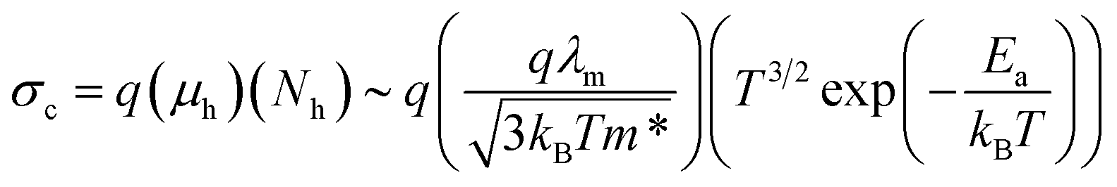
The electrical conductivity of p-type 3C–SiC can be defined as27,28
 | (1) |
As shown in Fig. 3(a), the resistance of 3C–SiC decreased up to 30% when the temperature increased from room temperature to 343 K and it continued to decrease until the carriers became fully ionized.28 A similar trend was also observed for low doped Si (which decreased up to 67% at 343 K, ESI†). However, for highly doped Si, the acceptors were almost fully ionized at room temperature. In addition, the ionized impurity scattering, the thermal vibration of the lattice, and collisions with free carriers would have significantly increased with the temperature and hence the mobility would have considerably decreased.27,29 As a result, conductivity would have decreased with temperature for highly doped Si (ESI†).
 | ||
| Fig. 3 The variation in resistance of 3C–SiC, due to (a) temperature (under dark conditions), and (b) illumination. | ||
Next, we investigated the influence of light illumination on the electrical conductance of all of the fabricated samples. When light is applied to a material, the carrier concentration of that material will change depending on its optical absorption coefficient (α).27,30,31
| α = (hν + Eg)γ | (2) |
As discussed in previous sections, under dark conditions, the resistivity of 3C–SiC decreases with temperature, hence a negative temperature coefficient (NTC) was observed (Fig. 4(a)). The transferred 3C–SiC resistor showed an NTC of −7508 to −6651 ppm K−1 for the temperature range of 297 to 343 K. Moreover, the TCR of 3C–SiC was not affected by variation in the wavelength and intensity of the incident light, Fig. 4(b). However, the TCR of low doped Si varied from 14.4 to 59.5% when the intensity increased from 0.5 to 2.0 mW cm−2.
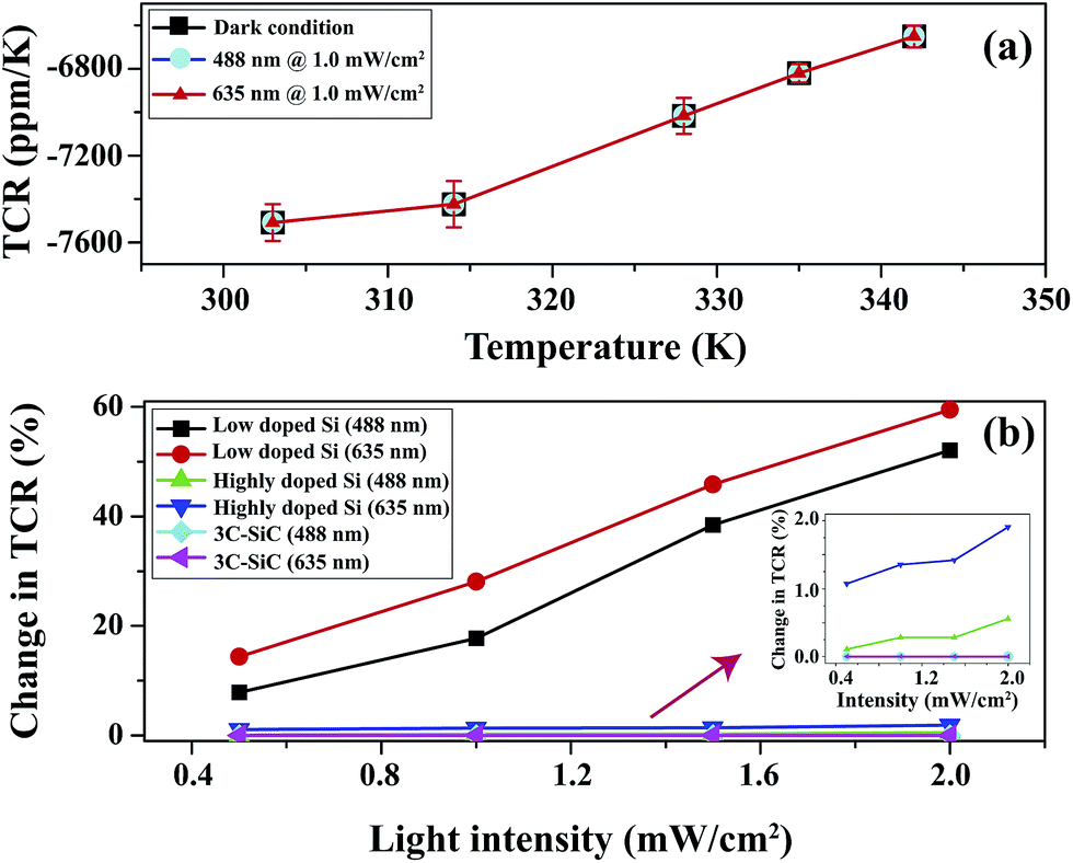 | ||
| Fig. 4 (a) Temperature coefficient of resistance of 3C–SiC under different light conditions and (b) the change of TCR at 326 K for low and highly doped Si, and 3C–SiC under dark conditions as a function of illumination intensity at 488 nm and 635 nm wavelengths. | ||
The TCR of low doped Si also varied 52% and 59.5%, at 2.0 mW cm−2 intensity and a temperature of 326 K, from dark conditions at 488 nm and 635 nm wavelength, respectively, implying that light of a 635 nm wavelength has more influence than a 488 nm wavelength source at the same intensity as shown in Fig. 4(b). This variation was observed because, at a higher photon energy, which is inversely proportional to the wavelength, the photon will be mainly absorbed near the surface which leads to the generation of dangling bonds and these bonds create trap states.34,35 As a result, non-radiative recombination of electrons and holes will be facilitated by the increase in photon energy. Therefore, at higher wavelengths, more free carriers will be generated in Si and hence the TCR for illumination at a 635 nm wavelength will be lower than that for a 488 nm wavelength. For highly doped Si, the effect of illumination on the TCR was reduced dramatically (0.5% and 1.9% change at 488 nm and 635 nm, respectively), indicating that the impurities were almost fully ionized at room temperature.
This article presents the characterization of the thermoresistive effect of 3C–SiC transferred onto a glass substrate, aiming at applications under visible light illumination. Benchmarking of the proposed 3C–SiC against conventional low doped and highly doped Si operating under the same conditions was also carried out. Experimental results and theoretical analysis showed that low doped Si had a high TCR of −17![[thin space (1/6-em)]](https://www.rsc.org/images/entities/char_2009.gif) 379 ppm K−1, but under light illumination the result varied significantly. Highly doped Si overcame this limitation; however, it had a considerably low TCR of 786 ppm K−1. On the other hand, p-type 3C–SiC grown on Si, which was subsequently transferred to a glass substrate, showed a relatively high TCR of −7508 ppm K−1 and the result was also independent of different light conditions. Therefore, taking advantage of the biocompatibility in SiC, 3C–SiC transferred onto a glass substrate can be an excellent platform for visible-light blind and highly sensitive temperature sensors working in light illuminated environments.
379 ppm K−1, but under light illumination the result varied significantly. Highly doped Si overcame this limitation; however, it had a considerably low TCR of 786 ppm K−1. On the other hand, p-type 3C–SiC grown on Si, which was subsequently transferred to a glass substrate, showed a relatively high TCR of −7508 ppm K−1 and the result was also independent of different light conditions. Therefore, taking advantage of the biocompatibility in SiC, 3C–SiC transferred onto a glass substrate can be an excellent platform for visible-light blind and highly sensitive temperature sensors working in light illuminated environments.
Acknowledgements
This work has been supported by the Australian Research Council (ARC) under Grant No. DP140100808. M. L. acknowledges the support of ARC-Decra No. DE130100304. This work was performed in part at the Griffith node of the Australian National Fabrication Facility. A company established under the National Collaborative Research Infrastructure Strategy to provide nano- and microfabrication facilities for Australia’s researchers.References
- T. A. Ulrich, E. M. Pardo and S. Kumar, Cancer Res., 2009, 69, 4167–4174 CrossRef CAS PubMed.
- Y. J. Kim, M. Tachibana, M. Umezu and Y. T. Matsunaga, J. Mater. Chem. B, 2016, 4, 1740–1746 RSC.
- G. Cesare, A. Nascetti and D. Caputo, Sensors, 2015, 15, 12260–12272 CrossRef PubMed.
- M. E. Castagna, S. Petralia, M. G. Amore, E. Cappello, A. Beninato, V. Sinatra, S. Baglio and S. Conoci, Sensing and Bio-Sensing Research, 2015, 6, 85–89 CrossRef.
- A. Agarwal, K. Buddharaju, I. K. Lao, N. Singh, N. Balasubramanian and D. L. Kwong, Sens. Actuators, A, 2008, 145146, 207213 Search PubMed.
- G. Steinhoff, O. Purrucker, M. Tanaka, M. Stutzmann and M. Eickhoff, Adv. Funct. Mater., 2003, 13, 841–846 CrossRef CAS.
- T. H. Park and M. L. Shuler, Biotechnol. Prog., 2003, 19, 243253 CrossRef PubMed.
- E. Lindner, V. V. Cosofret, S. Ufer, R. P. Buck, R. P. Kusy, R. B. Ash and H. T. Nagle, J. Chem. Soc., Faraday Trans., 1993, 89, 361–367 RSC.
- M. J. Madou and S. R. Morrison, Chemical sensing with solid state devices, Academic Press, New York, 1987 Search PubMed.
- U. G. Jung, K. Kuwana, Y. Ajiki, H. Takahashi, T. Kan, Y. Takei, K. Noda, E. Iwase, K. Matsumoto and I. Shimoyama, J. Micromech. Microeng., 2013, 23, 045015 CrossRef.
- A. Qamar, H. P. Phan, T. Dinh, L. Wang, S. Dimitrijev and D. V. Dao, RSC Adv., 2016, 6, 31191 RSC.
- H. P. Phan, T. Kozeki, T. Dinh, T. Fujii, A. Qamar, Y. Zhu, T. Namazu, N. T. Nguyena and D. V. Dao, RSC Adv., 2015, 5, 82121 RSC.
- H. W. Zheng, Y. L. Yan, Z. C. Lv, S. W. Yang, X. G. Li, J. D. Liu, B. J. Ye, C. X. Peng, C. L. Diao and W. F. Zhang, Appl. Phys. Lett., 2013, 102, 142409 CrossRef.
- S. Liu, H. Liu, Z. Huang, M. Fang, Y. G. Liu and X. Wu, RSC Adv., 2016, 6, 24267 RSC.
- N. Singha, K. Singha, A. Pandeyb and D. Kaur, Mater. Lett., 2016, 164, 28–31 CrossRef.
- T. Dinh, H. P. Phan, T. Kozeki, A. Qamar, T. Namazu, N. T. Nguyena and D. V. Dao, RSC Adv., 2015, 5, 106083 RSC.
- H. P. Phan, D. V. Dao, P. Tanner, L. Wang, N. T. Nguyen, Y. Zhu and S. Dimitrijev, Appl. Phys. Lett., 2014, 104, 111905 CrossRef.
- A. Qamar, H. P. Phan, J. Han, P. Tanner, T. Dinh, L. Wang, S. Dimitrijev and D. V. Dao, J. Mater. Chem. C, 2015, 3, 8804 RSC.
- U. Kalnins, A. Erglis, I. Dinne, I. Kumsars and S. Jegere, Med. Sci. Monit., 2002, 8, 1620 Search PubMed.
- S. Santavirta, M. Takagi, L. Nordsletten, A. Anttila, R. Lappalainen and Y. T. Konttinen, Arch. Orthop. Trauma. Surg., 1998, 118, 89–91 CrossRef CAS PubMed.
- P. Godignon, Mater. Sci. Forum, 2005, 483–485, 1009–1014 CrossRef CAS.
- L. Wang, S. Dimitrijev, J. S. Han, P. Tanner, A. Iacopi and L. Hold, J. Cryst. Growth, 2011, 329, 6770 CrossRef.
- D. V. Dao, H. P. Phan, A. Qamar and T. Dinh, RSC Adv., 2016, 6, 21302 RSC.
- H. P. Phan, P. Tanner, D. V. Dao, L. Wang, N. T. Nguyen, Y. Zhu and S. Dimitrijev, IEEE Electron Device Lett., 2014, 35, 399–401 CrossRef CAS.
- I. W. T. Chan, K. B. Brown, R. P. W. Lawson, A. M. Robinson, Y. Ma and D. Strembicke, Proc. IEEE Can. Conf. Elect. Comp. Eng., 1999, 1637–1642 Search PubMed.
- D. V. Dao, T. Toriyama, J. Wells and S. Sugiyama, Sens. Mater., 2003, 15, 113135 Search PubMed.
- S. M. Sze and K. K. Ng, Physics of Semiconductor Devices, Wiley, Hoboken, NJ, USA, 2007 Search PubMed.
- P. Norton, T. Braggins and H. Levinstein, Phys. Rev. B: Condens. Matter Mater. Phys., 1973, 8, 5632–5653 CrossRef CAS.
- R. S. Okojie, A. A. Ned, A. D. Kurtz and W. N. Carr, IEEE Trans. Electron Devices, 1998, 45, 785–790 CrossRef CAS.
- R. A. Soref and B. R. Bennett, IEEE J. Quantum Electron., 1987, 1, 123–129 CrossRef.
- R. H. Bube, Photoconductivity of Solids, John Wiley, New York, 1960 Search PubMed.
- J. Mullerova, S. Jurecka and P. Sutta, Sol. Energ., 2006, 80, 667–674 CrossRef.
- L. J. Liu, Y. M. Yiu and T. K. Sham, J. Phys. Chem. C, 2010, 114, 6966–6975 CAS.
- C. T. Sah, L. Forbes, L. L. Rosier and A. F. Tasch, Solid State Electron., 1970, 13, 759–788 CrossRef.
- R. G. Farrer, Solid State Commun., 1969, 7, 685–688 CrossRef CAS.
Footnote |
| † Electronic supplementary information (ESI) available. See DOI: 10.1039/c6ra19418d |
| This journal is © The Royal Society of Chemistry 2016 |