DOI:
10.1039/C6RA19355B
(Paper)
RSC Adv., 2016,
6, 94845-94850
Mechanical enhancement of a nanoconfined-electrodeposited nacre-like Cu2O layered crystal/graphene oxide nanosheet composite thin film†
Received
31st July 2016
, Accepted 26th September 2016
First published on 27th September 2016
Abstract
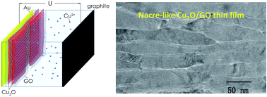
Graphene oxide (GO) based two dimensional (2D) nanosheets show great advantages for constructing nacre-like composites. Among the existing nacre structures, GO sheets were mostly used as hard inorganic components as those in nacre to improve the mechanical properties. Here, a novel nanoconfined electrodeposition process was explored to fabricate nacre-like Cu2O/graphene oxide (GO) thin films, where GO nanosheets functioned as the soft organic components in nacre. The inter-layer spaces between the GO nanosheets were used as templates for the growth of single crystalline Cu2O nanolayers, with thicknesses of several to tens of nanometers, though Cu2O belongs to the cubic phase. Due to the small lattice mismatch between the (1
0) plane of Cu2O and the (001) plane of GO, the Cu2O nanolayers most likely grew on the (001) plane of GO. The resulting nacre-like thin film demonstrates a 6 times greater hardness and a 3 times greater Young’s modulus, than those of pure GO thin films. This technique provides a promising route for the synthesis of nacre-like metal (metal-oxide)/GO composites.
Introduction
Although a free-standing graphene monolayer exhibits a high strength and stiffness with a Young’s modulus of about 1 TPa measured using nanoindentation,1,2 the graphene oxide (GO) monolayer has a Young’s modulus of only 250 ± 150 GPa,3 which was explained by the chemical bonding change due to oxidation and the presence of holes resulting from missing carbon atoms.4 As the number of GO layers increases to more than three, the Young’s modulus further decreases by an order of magnitude because of the thicker and shorter multilayers, where bending deflections are almost negligible and shear strains play a dominant role.3
Thus, it is desirable to improve the mechanical properties of multilayer GO-based composites. Compared with other approaches, one promising strategy is to fabricate the nacre-like structure,5–7 a 95 vol% of layered aragonite platelets bonded by a thin layer of organic material,8 by which the toughness of nacre could reach three orders of magnitude higher than that of calcium carbonate.9 Recently, graphene oxide nanosheets have shown the advantages of atom thick and flexible two dimensional structures, with plenty of surface functionalities, unique mechanical properties, and good dispersibility in solvents for constructing GO based nacre-like composite materials through different methods using various interface interaction designations for a significant enhancement in mechanical properties.10–15 For example, Teng et al.16 synthesized pyrene molecules with functional segmented pyrene poly(glycidylmethacrylate) (Py-PGMA), which was absorbed by graphene nanosheets through physical absorptions such as π–π stacking. Wan et al.17 demonstrated the integration of very strong and tough GO-based artificial nacre with chitosan through synergistic interactions of covalent and hydrogen bonding. Ming et al.18 fabricated nanocomposites of GO and montmorillonite nanosheets with poly(vinyl alcohol) via a vacuum-assisted filtering self-assembly process. Among these GO based nacre-like composites, GO nanosheets typically served as the inorganic components of nacre, rather than as the soft organic portion, to enhance the mechanical properties. However, because of the specific interface interactions, types of these composites are quite limited. In particular, GO-based nacre-like composites with hard blocks such as inorganic metals or metal oxides are rarely reported, due to the difficulty of forming uniform nacre-like structures.
The template-assisted nanoconfined electrodeposition process is a bottom-up technique, which has been widely used to prepare nanoparticles or one dimensional nanomaterials.19–22 But there have been no reports about the formation of two-dimensional (2D) nanomaterials using 2D template-assisted electrodeposition so far, especially for native non-layered crystals. Further research demonstrates that crystal structure and growth in 2D spaces are quite different from bulk crystals.23 Actually, previous works have shown crystals in 2D confined spaces usually grow into individual nanosheets24 or nanoparticles,25 which cannot be classified as 2D materials in a strict sense because of their limited size. The inter-layer spaces between GO thin films are quite narrow, crystals would prefer to grow on the surfaces rather than into the GO nanosheets. So it is still hard to fabricate a well nacre-like GO thin film with interlayer spaces filled up with inorganic components.
In this work, for the first time, we have successfully fabricated a nacre-like Cu2O/GO composite thin film with enhanced mechanical properties through a nano-confinement electrochemical deposition process, using the nanospaces between the GO sheets as templates. Due to the nano-confinement, Cu2+ ions diffused into the 2D spaces and when reduced turned into 2D sheet-like single crystals, until the inter-spaces were fully occupied, though Cu2O belongs to the cubic system. This indicates that native non-layered crystals (cubic crystals) can be turned into 2D sheet-like single crystals using this process. Different from the reported graphene-based artificial nacre nanocomposites, Cu2O crystals here are designed to serve as “bricks”, which improve the hardness and strength of GO thin films when subjected to shear forces. The hardness and Young’s modulus are 6 times and 3 times higher than those of the original GO thin film, respectively. This electrodeposition method may provide a new way to fabricate other nacre like metal (metal-oxide)/GO composite thin films.
Experimental
Materials and chemicals
Graphite powder (99.95%) was obtained from Aladdin. H2SO4 (95–98%), NaNO3, KMnO4, H2O2 (30 wt%), and HCl (36–38%) were purchased from Sinopharm Chemical Reagent Co., Ltd. All chemicals were used as received without further purification. Polyethersulfone (PES) membranes (Whatman) with a pore size of 200 nm were used for the formation of the GO films using filtration. The electrodeposition was conducted on a DC Regulated Power Supply (Zhaoxin PS-503D). The deionized water (18.2 MΩ cm) used throughout all the experiments was produced using a Millipore Direct-Q System.
Synthesis of the GO thin films
In a typical procedure, GO was prepared from graphite powder using a modified Hummer’s method.26 Briefly, 0.5 g of natural graphite powder was added to 11.5 mL of H2SO4 under stirring at about 0 °C, and then 1.5 g of NaNO3 and 1.5 g of KMnO4 were added sequentially. Successively, the mixture was transferred to a water bath at 30 °C and stirred for 1 hour to form a thick paste. Then, 23 mL of distilled water was slowly added and the temperature was increased to 98 °C. After aging for 30 min, an additional 500 mL of water was added, followed by the slow addition of 20 mL of H2O2 (30 wt%). The mixture was filtered and washed with diluted HCl aqueous (1/10 v/v) to remove metal ions, and this was followed by washing with distilled water several times. Then the GO was collected and dried under vacuum at 60 °C for 6 hours. A certain amount of GO was first exfoliated in distilled water (0.2 mg mL−1) with ultrasonic treatment to form a stable GO nanosheet suspension. The pH of the suspension was adjusted close to 6.2 using dilute HCl and NaOH. The GO thin films supported on PES porous substrates were prepared by filtering the above 1 mL of GO suspension on the PES membranes.
Synthesis of nacre-like Cu2O/GO composite thin films using electrodeposition
As shown in Fig. S1,† first, a thin layer (about 10–15 nm) of Au was sputtered on the surface of the GO thin films of the preformed GO thin film on PES by using a Hitachi e-1030 ion sputter at a pressure of 10 Pa and a current density of 10 mA. The bottom PES was sealed with an insulating plastic ring (nitrile butadiene rubber) and later directly contacted with the electrolyte. This GO thin film/PES was then mounted in an electrochemical cell to serve as the cathode. The anode was graphite. The electrolyte is composed of 0.01 M copper sulphate and 0.05 M boric acid with a pH value of 5. A constant potential of −1.5 V (vs. Ag/AgCl) was applied. The electrodepositing process is illustrated in Scheme 1 and Fig. S1.† In this work, three samples, named Cu2O/GO-1.5, Cu2O/GO-3, and Cu2O/GO-24, were fabricated with three different deposition times of 1.5, 3 and 24 hours, respectively.
 |
| Scheme 1 Illustration of the preparation process of the nacre-like Cu2O/GO composite thin film. | |
Characterization
The phases of the as-prepared products were characterized using X-ray diffraction (XRD) at room temperature using an X’ Pert PRO (PANalytical, Netherlands) instrument with Cu Kα radiation. The morphologies and structures were characterized using scanning electronic microscopy (SEM) (Hitachi S-4800) and transmission electron microscopy (TEM) (Tecnai G2 F20 S-TWIN, FEI) with an accelerating voltage of 200 kV. The cross-section samples for the TEM were prepared using a focused ion beam (FIB) (Quanta 3D FEG, FEI) through a “H-bar lift-out” method. First, a Pt protective layer was deposited on the surface of the sample. Then the cross-section slice of Cu2O/GO was cut free from the sample (30 kV) and glued on the TEM grid using a micro-manipulator. The sample was further thinned in the FIB (2–5 kV) until it was thinner than 100 nm. The mechanical properties were characterized using a nanoindenter (Agilent G200). A Berkovich tip with the shape of a three-sided pyramid was used in the experiments. The contact area A = 24.6h2 + 575h, where h is contact depth.
Results and discussion
Morphology and structures
The XRD patterns of the PES porous substrates, GO thin film on the PES substrate before electrodeposition, Cu2O/GO-1.5, Cu2O/GO-3 and Cu2O/GO-24 are shown in Fig. 1. A character diffraction peak at about 2θ = 9° is detected for the GO thin film on PES. This is assigned to the (001) peaks of GO, indicating the formation of the layered structure of a GO film with a d-spacing of 1.024 nm, comparable to the reported distance of layered GO.27 It is noticed that the (001) peaks of GO were shifted to lower angles by increasing the deposition time. This means the interplanar distance of the GO increases, due to the formation of Cu2O which expands the interplanar spaces of the GO sheets more and more with longer deposition times. In the Cu2O/GO composite films, diffraction peaks of standard Cu2O (JCPDS standard card no. 65-3288) are detected. Small diffraction peaks from pure Cu appear in the Cu2O/GO-24 sample, indicating that the Cu2+ ions in the electrolyte are almost consumed and the pre-deposited Cu2O were further reduced to Cu. While the relative peak intensity of Cu2O (111) vs. (200) changes with deposition time. This might be due to that at the beginning more oriented growth of Cu2O sheets were formed and stacked along the 〈001〉 direction, but Cu2O sheets are randomly packed to each other when increasing the deposition time. Then the preferred orientation disappeared and the (111) peak dominates in the Cu2O powders.
 |
| Fig. 1 XRD patterns of the PES substrate, GO thin film with PES substrate, GO/Cu2O-1.5, GO/Cu2O-3 and GO/Cu2O-24. | |
Fig. 2a shows the cross-section SEM image of the GO thin film. It is clear that the prepared GO thin film (about 500 nm) has good lamellar structures, which provide the 2D confined inter-layer growing spaces for Cu2O. Further experiments prove that without the 2D templates of the GO thin films, cubic Cu2O crystals grow directly on the surface of the gold layer (of a PES substrate), as shown in Fig. S2 and S3.† Fig. 2b–f show the cross sections of Cu2O/GO-1.5, Cu2O/GO-3 and Cu2O/GO-24, respectively. Flat sheet-like Cu2O crystals grow between the GO sheets gradually from the Au side, expanding the interlayer space between the GO sheets. With the extension of deposition time, in Fig. 2c and e, more interlayer spaces are filled with Cu2O crystals. After 24 hours of deposition in Fig. 2f, the whole GO thin film is packed with Cu2O crystals and the membrane thickness increases obviously, which also breaks the expected nacre-like structure of the Cu2O/GO composite thin films. Therefore, the optimal electrodeposition time is 3 hours to get good nacre-like structures. Actually, uniformly growing crystals into the spaces in GO thin films rapidly is still a great challenge for this process. The diffusion of Cu2+ into the GO spaces and the conductivity of the GO and the pre-deposited Cu2O should have an influence on the subsequence deposition. It might be possible expand the spaces in the GO thin films by interpenetrating nanowires to get a more uniform nacre-like structure with a short electrodeposition time.
 |
| Fig. 2 Cross-section SEM images of (a) the pure GO thin film, (b and c) Cu2O/GO-1.5, (d and e) Cu2O/GO-3 and (f) Cu2O/GO-24; (c) and (e) are magnified SEM images of (b) and (d), respectively, showing nacre-like structures of Cu2O/GO. | |
To further characterize the nacre-like structure and morphology, the cross-section slice of the Cu2O/GO-3 sample was studied using TEM. The TEM image of the entire cross section of Cu2O/GO-3 (Fig. 3a) shows that the GO sheets are separated by layered Cu2O crystals with thicknesses of several to tens of nanometers and the interlayer spaces increase accordingly. Four selected areas (marked by b–e) were further studied using magnified HRTEM images, exhibiting the structures at the atomic scale. Clear lattice fringes are observed as shown in Fig. 3b. The interlayer spaces packed with Cu2O single crystals were reflected in the spotty FFT patterns.
 |
| Fig. 3 Low magnification cross-section TEM images of the as-prepared Cu2O/GO-3 (a) and TEM images with higher magnification (b–e) of the given areas from (a); the directions of the crystal planes are marked in (b–e), as well as the inter-planar spaces. The insets are the corresponding FFT patterns. | |
It is found that the thickness of the GO sheets differ in different parts of the sample. For thin GO sheets (<0.7 nm) as in Fig. 3c, the Cu2O single crystals grow straight across the GO sheets and its growth direction remains the same. For thick GO sheets (>0.7 nm) as in Fig. 3b and d, the Cu2O will be divided into two twin-like crystals by the GO sheets. These twin-like single crystals grow symmetrically onto the GO sheets, with a relation to the Cu2O crystals (1
0) oriented on the GO (001) plane. In addition, no matter how thick the GO sheets are, the mentioned Cu2O crystals are all (1
0) oriented on the GO (001) plane, as marked by the circles in Fig. 3b–d. One exceptional case was found in Fig. 3e, where a triangular zone was formed by the GO sheets. As a result of the concentration of the stress in this triangular zone, Cu2O crystals are all (001) oriented on the GO (001) plane.
Growth mechanism
To explain this growth phenomenon, one scenario for the electro-deposition process is illustrated in Fig. 4a. Cu2+ ions travel through the interspace of the GO sheets, and are reduced from the bottom layer of the GO sheets. The electrodeposition starts from certain “pure-graphene” regions without functional groups, which are actually conductive. In addition, tiny pores might also exist on the GO nanosheets. Cu2+ ions are firstly reduced in these pores (directly contacted with the Au layer). When the tiny pores are filled up, nucleation and growth of the Cu2O crystals occurs at these spots. After the bottom interspaces of the GO sheets are occupied, Cu2O crystals begin to grow in the upper spaces.
 |
| Fig. 4 Schematic illustration of (a) the cross section of the Cu2O/GO nacre structure; (b) the coincident periodic match mode of the Cu2O on the GO plane. | |
In order to study the mechanism of Cu2O crystal growth on the GO (001) plane, lattice mismatch between the Cu2O and GO plane was calculated, as shown in Fig. 4b. The values of the lattice mismatch fm can be calculated using the equation below:28
|
 | (1) |
where
ae and
as are the lattice parameters of the epilayer and the substrate, respectively. Using the following lattice constants,
aCu2O(1
0) = 0.298 nm,
aCu2O(001) = 0.352 nm and
aGO(001) = 0.246 nm,
29 the lattice mismatch between Cu
2O (1
![[1 with combining macron]](https://www.rsc.org/images/entities/char_0031_0304.gif)
0) and GO (001) [
fm = (5
aCu2O − 6
aGO)/6
aGO] is estimated to be 0.95%, which is smaller than the 2.21% between Cu
2O (001) and GO (001) [
fm = (5
aCu2O − 7
aGO)/7
aGO]. This result is consistent with the experimental observations in
Fig. 3b and c,
i.e., Cu
2O crystals most likely orientate along (1
![[1 with combining macron]](https://www.rsc.org/images/entities/char_0031_0304.gif)
0) on GO (001).
Mechanical performance
The mechanical properties of the mentioned samples were tested using nanoindentation. The corresponding load-displacement curves of the samples are shown in Fig. 5. Hardness and the elastic modulus were calculated from the nanoindentation results, using the following equations:30 |
 | (2) |
|
 | (3) |
|
 | (4) |
where S, Eeff, H are stiffness, effective elastic modulus and hardness, respectively. P designates the load and h the displacement relative to the initial undeformed surface. A refers to the contact area.
 |
| Fig. 5 The loading/unloading curves recorded from GO, GO/Cu2O-1.5, GO/Cu2O-3 and GO/Cu2O-24 using nanoindentation. | |
The results are listed in Table 1. The values of the Young’s modulus and hardness are the average values of 5 measured points with errors of about 15%. The nacre-like structure of the composite thin film strengthens the GO when subjected to shear forces. All electrodeposited samples have better performances than the pure GO thin film. The Cu2O/GO-3 sample is the best in terms of hardness with 5.7 GPa and a Young’s modulus of 31.1 GPa while pure GO sheets only have a hardness of 0.8 GPa and a Young’s modulus of 8.5 GPa. Therefore, the strategy to fabricate nacre-like Cu2O/GO composite thin films reported here is an effective way to improve the mechanical properties of GO sheets. The Young’s moduli of our GO samples are relatively lower than those reported (44.6 to ≈8.5 GPa,31 695 ± 53 to 697 ± 15 GPa,32 and 0.008 to 0.25 Tpa (ref. 3)) for multilayer GO thin films. The wide variation of Young’s modulus for the GO thin films might be due to the different measurement methods, the measuring environment and the quality of the GO samples.
Table 1 Computed hardness, elastic modulus and displacement of the samples at max loada
Sample |
Modulus at max load/GPa |
Hardness at max load/GPa |
Disp at max load/nm |
The data are the average values of 5 measured points with error about 15%. |
Cu2O/GO-1.5 |
17.057 |
1.361 |
249.535 |
Cu2O/GO-3 |
31.078 |
5.68 |
148.741 |
Cu2O/GO-24 |
13.407 |
1.394 |
262.528 |
GO |
8.475 |
0.831 |
337.353 |
Conclusions
In summary, nacre-like Cu2O/GO composite thin films were obtained using a nanoconfined electrodeposition method, using the 2D nanospaces between the GO nanosheets as templates. Native non-layered Cu2O nanolayers most likely orientated along the 〈1
0〉 direction on the GO (001) plane, due to the lowest lattice mismatch. The nacre-like Cu2O/GO composite thin films show significantly enhanced hardness and Young’s modulus with 6 times and 3 times that of pure GO thin films, respectively. This provides a novel and simple route for the preparation of nacre-like metal (metal-oxide)/GO composite thin films. However, uniformly growing crystals into the spaces of the GO thin films rapidly is still a great challenge for this process. It might be possible to expand the spaces in the GO thin films by interpenetrating nanowires to get a more uniform nacre-like structure with a short electrodeposition time.
Acknowledgements
This work was supported by the National Basic Research Program of China 973 Program (2015CB655302), the Natural Science Foundation for Outstanding Young Scientist of Zhejiang Province, China (LR14E020001) and the National Natural Science Foundations of China (NSFC 21271154).
Notes and references
- C. Lee, X. Wei, J. W. Kysar and J. Hone, Science, 2008, 321, 385–388 CrossRef CAS PubMed.
- F. Liu, P. Ming and J. Li, Phys. Rev. B: Condens. Matter Mater. Phys., 2007, 76, 064120 CrossRef.
- C. Gómez-Navarro, M. Burghard and K. Kern, Nano Lett., 2008, 8, 2045–2049 CrossRef PubMed.
- J. T. Paci, T. Belytschko and G. C. Schatz, J. Phys. Chem. C, 2007, 111, 18099–18111 CAS.
- H. B. Yao, J. Ge, L. B. Mao, Y. X. Yan and S. H. Yu, Adv. Mater., 2014, 26, 163–188 CrossRef CAS PubMed.
- H. B. Yao, H. Y. Fang, Z. H. Tan, L. H. Wu and S. H. Yu, Angew. Chem., 2010, 122, 2186–2191 (Angew. Chem., Int. Ed., 2010, 49, 10127–10131) CrossRef.
- H.-P. Cong, J.-F. Chen and S.-H. Yu, Chem. Soc. Rev., 2014, 43, 7295–7325 RSC.
- U. G. Wegst, H. Bai, E. Saiz, A. P. Tomsia and R. O. Ritchie, Nat. Mater., 2015, 14, 23–36 CrossRef CAS PubMed.
- M. A. Meyers, P.-Y. Chen, A. Y.-M. Lin and Y. Seki, Prog. Mater. Sci., 2008, 53, 1–206 CrossRef CAS.
- D. A. Dikin, S. Stankovich, E. J. Zimney, R. D. Piner, G. H. Dommett, G. Evmenenko, S. T. Nguyen and R. S. Ruoff, Nature, 2007, 448, 457–460 CrossRef CAS PubMed.
- T. Gong, S. Won, J.-H. Kim, H.-J. Lee, C. Lee and S.-M. Lee, Chem. Commun., 2015, 51, 2671–2674 RSC.
- Y. Xu, H. Bai, G. Lu, C. Li and G. Shi, J. Am. Chem. Soc., 2008, 130, 5856–5857 CrossRef CAS PubMed.
- Y. Gao, L.-Q. Liu, S.-Z. Zu, K. Peng, D. Zhou, B.-H. Han and Z. Zhang, ACS Nano, 2011, 5, 2134–2141 CrossRef CAS PubMed.
- Y. Zhang, S. Gong, Q. Zhang, P. Ming, S. Wan, J. Peng, L. Jiang and Q. Cheng, Chem. Soc. Rev., 2016, 45, 2378–2395 RSC.
- X. Huang, X. Qi, F. Boey and H. Zhang, Chem. Soc. Rev., 2012, 41, 666–686 RSC.
- C.-C. Teng, C.-C. M. Ma, C.-H. Lu, S.-Y. Yang, S.-H. Lee, M.-C. Hsiao, M.-Y. Yen, K.-C. Chiou and T.-M. Lee, Carbon, 2011, 49, 5107–5116 CrossRef CAS.
- S. Wan, J. Peng, Y. Li, H. Hu, L. Jiang and Q. Cheng, ACS Nano, 2015, 9, 9830–9836 CrossRef CAS PubMed.
- P. Ming, Z. Song, S. Gong, Y. Zhang, J. Duan, Q. Zhang, L. Jiang and Q. Cheng, J. Mater. Chem. A, 2015, 3, 21194–21200 CAS.
- J. Yang, X. Shen, Z. Ji, H. Zhou, G. Zhu and K. Chen, Ceram. Int., 2015, 41, 4056–4063 CrossRef CAS.
- J. M. Lee and J. S. Ko, J. Mater. Sci., 2015, 50, 393–402 CrossRef CAS.
- Y. Wang, L. Zhang, G. Meng, X. Peng, Y. Jin and J. Zhang, J. Phys. Chem. B, 2002, 106, 2502–2507 CrossRef CAS.
- O. Yalçın, G. Kartopu, H. Çetin, A. Demiray and S. Kazan, J. Magn. Magn. Mater., 2015, 373, 207–212 CrossRef.
- G. Algara-Siller, O. Lehtinen, F. Wang, R. Nair, U. Kaiser, H. Wu, A. Geim and I. Grigorieva, Nature, 2015, 519, 443–445 CrossRef CAS PubMed.
- L. Wang, Y. Zhu, J.-Q. Wang, F. Liu, J. Huang, X. Meng, J.-M. Basset, Y. Han and F.-S. Xiao, Nat. Commun., 2015, 6, 6957, DOI:10.1038/ncomms7957.
- W. Lu, R. Ning, X. Qin, Y. Zhang, G. Chang, S. Liu, Y. Luo and X. Sun, J. Hazard. Mater., 2011, 197, 320–326 CrossRef CAS PubMed.
- W. S. Hummers Jr and R. E. Offeman, J. Am. Chem. Soc., 1958, 80, 1339 CrossRef.
- X. Wang, S. Liu, H. Wang, F. Tu, D. Fang and Y. Li, J. Solid State Electrochem., 2012, 16, 3593–3602 CrossRef CAS.
- M. Kaya and Y. Atici, Superlattices Microstruct., 2004, 35, 35–44 CrossRef CAS.
- Q. Hua, T. Cao, H. Bao, Z. Jiang and W. Huang, ChemSusChem, 2013, 6, 1966–1972 CrossRef CAS PubMed.
- W. C. Oliver and G. M. Pharr, J. Mater. Res., 2004, 19, 3–20 CrossRef CAS.
- T. Gong, D. V. Lam, R. Liu, S. Won, Y. Hwangbo, S. Kwon, J. Kim, K. Sun, J.-Y. Kim, S.-M. Lee and C. Lee, Adv. Funct. Mater., 2015, 25, 3756–3763 CrossRef CAS.
- S.-H. Kamg, T.-H. Fang, Z.-H. Hong and C.-H. Chuang, Diamond Relat. Mater., 2013, 38, 73–78 CrossRef.
Footnote |
† Electronic supplementary information (ESI) available: Additional SEM images and XRD results. See DOI: 10.1039/c6ra19355b |
|
This journal is © The Royal Society of Chemistry 2016 |
Click here to see how this site uses Cookies. View our privacy policy here.