Monohydride signature as a key predictor of successful Si(110) surface functionalization

A. Guptaa, J. P. Bruce b, K. McEleneybc, M. S. Freund bc and D. R. Oliver*ac
aDepartment of Electrical and Computer Engineering, University of Manitoba, R3T 5V6, Winnipeg, Manitoba, Canada. E-mail: derek.oliver@umanitoba.ca
bDepartment of Chemistry, University of Manitoba, R3T 2N2, Winnipeg, Manitoba, Canada
cManitoba Institute for Materials, University of Manitoba, R3T 2N2, Winnipeg, Manitoba, Canada

Received 14th July 2016 , Accepted 6th September 2016

First published on 7th September 2016


Abstract

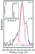
Methyl-terminated (110)-oriented silicon surfaces have been prepared from monohydride-terminated, H–Si(110) surfaces using a chlorination/alkylation procedure. Transmission infrared spectroscopy of the H–Si(110) surfaces showed absorption features indicating monohydride structures along the [−110] direction. X-ray photoelectron spectroscopy was used to characterize the methyl-terminated, CH3–Si(110), surfaces. Surface coverage calculations revealed 0.83 of an equivalent monolayer coverage for methyl-terminated Si(110) surfaces. No oxidation of silicon was observed in the high-resolution Si 2p spectra and the samples were stable against oxidation over time, with only 0.2 of a monolayer of surface oxide observed a month after the sample preparation. Thus, the chlorination/alkylation procedure can be used for the functionalization of monohydride Si(110) surfaces with improved long term stability.


Introduction

Micron-scale high aspect ratio silicon structures (microwires) have drawn significant attention as building blocks for artificial photosynthetic devices.1–3 One envisioned device consists of two sets of microwire arrays connected in series to provide the necessary photovoltage to drive the water-splitting reactions.1,2 The two microwire arrays are separated by a membrane that must support both ionic and electronic charge transfer.4 Surface chemistry of the microwires directly affects charge transport near the wire surface and at the microwire/membrane junction, both of which impact the overall device efficiency.2 Oxidation of the silicon surface introduces an additional electrical barrier which increases the microwire–membrane junction resistance, decreasing the available photovoltage to drive the redox reactions.2,3 Various functionalization methods have been developed to mitigate the problem of surface oxidation and introduce desired chemical and electrical properties to the silicon surface.3,5–8 Of these, surface functionalization with methyl groups has been shown to provide long term stability against oxidation, making this a promising approach to passivating the microwires.3,7

Linford et al. demonstrated that alkyl monolayers can be attached to hydrogen-terminated Si(100) and Si(111) surfaces by thermal decomposition of diacyl peroxides.8 Following their work, several functionalization methods were proposed including two-step chlorination/alkylation, UV-mediated hydrosilylation, electrochemical attachment of hydrocarbon monolayers, etc.8–10 Of these, the two-step chlorination/alkylation method (Fig. 1) is the only wet chemical functionalization method that allows attachment of methyl monolayers on a hydrogen-terminated silicon surface.9–13 In this method, a hydrogen-terminated silicon surface is reacted with PCl5-saturated chlorobenzene solution containing a radical initiator followed by reaction with Grignard (CH3MgBr) or methyl-lithium (CH3Li) reagent to get a uniform monolayer of methyl groups.7,10,13 The other methods generally involve addition of larger organic groups containing double or triple bonds which can directly attach to the free radicals created due to the homolytic cleavage of Si–H bonds.8,9


image file: c6ra18009d-f1.tif
Fig. 1 Schematic representation of methyl-termination of a silicon surface using a two-step chlorination/alkylation procedure.

Previous studies have examined the Si(111) surface where the distance between silicon atoms is 3.8 Å.10,11 Thus, methyl groups, with a van der Waals diameter of 2.3–2.5 Å, are capable of completely passivating all the available silicon sites on the surface.11–13 These studies of (111)-oriented, planar silicon surfaces have been used as a basis for the presumption that these functionalization techniques may be directly implemented for the multi-faceted silicon microwires.14 However, these microwire structures consist mostly of {110}-oriented surfaces with different surface atom densities and bonding structure: parameters that directly influence the achievable surface coverage and potentially the stability.14,15 It has been observed that H-termination of (111) and (110)-oriented surfaces involve different surface preparation strategies16–18 which can directly affect the surface coverage after methylation, as seen in case of functionalized Si(111) surfaces prepared using different etching methods.19 Using an etching procedure that is not optimized for the majority of the surface will lead to faster oxidation times and compromised device performance, especially considering minority charge carriers are collected at these interfaces.2,3 Thus, the surface preparation strategies need to be developed and optimized specifically to yield better stability against oxidation for (110)-oriented surfaces as these hold the key to stable/improved device performance for systems based on VLS-grown silicon microwire arrays.

The ideal H-terminated Si(110) surface can be represented as a rectangular unit cell (two-dimensional space group pg).16–18 The interatomic distance for the 〈100〉 and 〈110〉 directions (i.e. the sides of the rectangle) are 5.4 Å and 3.8 Å respectively.17 The fifth Si atom within the unit cell lies in the plane of the space group and is bonded to two of the corner atoms (Si bond length ∼2.35 Å). This geometry provides sufficient space for the hydrogen atoms that are bonded to each of the five silicon atoms. However, steric hindrance due to the comparable size of the methyl group and the silicon bond length could cause incomplete substitution/coverage for the case of an Si(110) surface.

We report surface coverage studies of (110)-oriented, planar methyl-terminated silicon surfaces prepared using a chlorination/alkylation procedure. Transmission infrared spectroscopy (TIRS) was used to analyse the hydrogen-terminated surface used for functionalization, while X-ray photoelectron spectroscopy (XPS) was used to investigate the surface coverage and oxidative stability of the functionalized surface.

Experimental

Sample preparation

Boron-doped, p-type, (110)-oriented, silicon wafers (ρ > 60 Ω cm, thickness 350 μm, Virginia Semiconductor, Inc.) were first cut into small rectangular pieces (∼2 cm × 0.5 cm) and cleaned with a 4[thin space (1/6-em)]:[thin space (1/6-em)]1 (v/v) H2SO4 (18 M)[thin space (1/6-em)]:[thin space (1/6-em)]H2O2 (30 vol%), piranha solution that was kept at 95–100 °C (caution: piranha solution can be extremely hot and dangerous, needs to be handled very carefully) for 10 minutes followed by a deionized water (Millipore, 18.3 MΩ cm) rinse for 10 minutes. The wafer was then dried with Ar(g) and stored to be used later. The cleaned wafer was rinsed with methanol, acetonitrile and water sequentially and dried with Ar(g) before it was etched with a 1[thin space (1/6-em)]:[thin space (1/6-em)]1[thin space (1/6-em)]:[thin space (1/6-em)]98 (v/v/v) HF (49 vol%)[thin space (1/6-em)]:[thin space (1/6-em)]H2O2 (30 vol%)[thin space (1/6-em)]:[thin space (1/6-em)]H2O solution for 5 minutes, subsequently rinsed with deionized water (bubbled with Ar(g) for about 30 minutes to reduce the oxygen content) for 10 minutes and finally dried with Ar(g) to produce a monohydride terminated, H–Si(110) surface.18

The monohydride-terminated sample was transferred to an N2(g) purged glove box where it was reacted with a phosphorous pentachloride (PCl5)-saturated, anhydrous chlorobenzene (99.8%, Sigma-Aldrich) solution with a small amount of benzoyl peroxide initiator at 90 °C for 45 minutes to obtain a chlorine-terminated, Cl–Si(110) surface. The sample was then rinsed with anhydrous chlorobenzene and anhydrous tertahydrofuran (THF, ≥99.9%, Sigma-Aldrich). The resulting Cl–Si(110) surface was reacted with 1.6 M methyl-lithium reagent (Sigma-Aldrich) in THF at 60 °C for a minimum of three hours to produce a methyl-terminated, CH3–Si(110) surface.7 The now-methylated sample was then cleaned with anhydrous THF followed by rinsing with anhydrous methanol (99.8%, Sigma-Aldrich) and removed from the chamber in the anhydrous methanol solution. The sample was then sonicated sequentially with methanol, acetonitrile and deionized water for five minutes each and finally dried with Ar(g).

Instrumentation

Transmission infrared spectroscopy (TIRS). A Thermo Electron Nicolet 6700 FT-IR spectrometer purged with N2(g), was used to collect the infrared spectra. A H–Si(110) sample was placed into the sample holder so that the infrared light was incident at the Brewster angle (74°) from the surface normal. This geometry is sensitive to vibrational modes that are parallel and perpendicular to the surface.20 A liquid-nitrogen cooled, mercury cadmium telluride (MCT) detector was used and infrared spectra were collected with a resolution of 4 cm−1 averaging over 1000 scans. Omnic software was used to collect the TIRS data and subsequent data processing.
X-ray photoelectron spectroscopy (XPS). The XPS spectra were collected on a Kratos Axis Ultra DLD XPS spectrometer with a base pressure of 10−9 Torr. Al Kα (1486.6 eV) monochromatic X-rays generated with 10 mA emission current and 15 kV anode voltage were used to excite the photoelectrons. Charge neutralization was not required as the samples were sufficiently conductive that charge build-up was not an issue. All spectra were collected in a fixed analyzer transmission mode. Survey scans were collected with a pass-energy of 160 eV and high resolution scans were collected with a pass-energy of 20 eV. Peak-fits for the high resolution XPS spectra were obtained using CasaXPS. Peak positions in the C 1s region were referenced to adventitious carbon peak with a binding energy of 285 eV and while in the Si 2p region were referenced to the bulk Si peak (99 eV).

Surface coverage was calculated using the substrate-overlayer model.11,21,22 According to the model, an equivalent fractional monolayer, Φov can be calculated as:

 
image file: c6ra18009d-t1.tif(1)

In the above equation, Iov/ISi is the intensity ratio of the peak areas of surface overlayer to the bulk silicon (Si 2p). θ is the angle used for the collection of the electrons (0° with respect to surface normal) in our instrument. ρSi (2.328 g cm−3) is the density of silicon and ρov is the density of the overlayer (3 g cm−3 for C).11 SFSi (0.328) and SFov (0.278 for C 1s) are the corresponding sensitivity factors for silicon and the overlayer atoms respectively. a is the atomic diameter for the overlayer (0.19 nm for C) atoms and λ is the escape depth for the electrons through the overlayer with the assumption that λov = λSi for our calculations.11,22 For a methyl overlayer, the escape depth was taken to be 3.5 nm.21,22

Results

Fig. 2 shows the TIR spectrum obtained for the H–Si(110) surface. Two peaks were observed at wavenumbers, 2089 cm−1 and 2070 cm−1 corresponding to the in-phase and out of phase Si–H stretch respectively.16 These stretching-modes correspond to the coupled-monohydride structures along [−110] direction.16–18,23
image file: c6ra18009d-f2.tif
Fig. 2 TIR spectrum for the H–Si(110) surface obtained at an incident angle of 74° and a resolution of 4 cm−1. The two peaks correspond to the Si–H stretch corresponding to long chain monohydride-step structure along [−110] direction. The reference was obtained from a piranha-cleaned, oxidized sample.

The XPS survey scan (Fig. 3) contains peaks that correspond to O 1s (531 eV), C 1s (285 eV), Si 2s (149 eV) and Si 2p (99 eV).7,21 Peaks corresponding to Cl 2s (270 eV) and Cl 2p (200 eV) region appeared for the Cl–Si(110) surface confirming the presence of the chlorine overlayer.


image file: c6ra18009d-f3.tif
Fig. 3 XPS survey spectra for hydrogen-(red), chlorine-(blue), and methyl-terminated (green) Si(110) surfaces. The surfaces mainly showed peaks corresponding to silicon and adventitious carbon and oxygen. Cl 2s and Cl 2p peaks appeared when the hydrogen-terminated surface had been reacted with PCl5 and were absent for a methyl-terminated surface.

After methyl functionalization, the chlorine peaks were absent in the survey spectrum indicating that the chlorine overlayer was completely removed during the methylation procedure. No fluorine (686 eV) peak was observed indicating that the samples were clean after the rinsing process and there was no residual fluorine from the etching procedure.

High resolution XPS spectrum (Fig. 4) of the Si 2p region shows signals corresponding to the bulk silicon substrate with Si 2p3/2 and Si 2p1/2 peaks. For the chlorine-terminated sample, an additional peak was observed corresponding to Si–Cl bonds.7 For hydrogen-terminated and methyl-terminated samples the shift in binding energy was not significant enough to distinguish between bulk and surface silicon features. The absence of any feature around 101–103 eV corresponding to silicon oxide indicates that there was no oxidation of the surface during the reaction within the detection limit of the instrument.7,21


image file: c6ra18009d-f4.tif
Fig. 4 High resolution XPS spectra of Si 2p region for (a) H-terminated (b) Cl-terminated and (c) CH3-terminated Si(110) surfaces. The spectra were fit to have two peaks (red) corresponding to the spin split states, Si 2p3/2 and Si 2p1/2. The Cl-terminated spectrum had an additional peak (blue) that is shifted in binding energy due to the surface overlayer. No silicon oxide peaks were observed in the 101–103 eV region.

High resolution XPS spectrum of the C 1s region for the CH3–Si(110) surface (Fig. 5) shows a peak corresponding to the carbon bonded to the surface silicon (C–Si, B.E. = 283.7 eV) in addition to the peaks associated with adventitious carbon. The adventitious carbon peak at 285 eV can be attributed to hydrocarbons while the peak at 286.5 eV to oxidized carbon species.10 The changes in intensity and broadening of these adventitious peaks represent variations in the number of adventitious hydrocarbons on the surface and are also dependent on the chemical nature of these species. Using the surface overlayer model (eqn (1)), an average (6 different samples) monolayer coverage of 0.83 ML (standard deviation = 0.04, IC–Si/ISi 2p = 0.049) was calculated for the CH3–Si(110) surfaces, which is in excellent agreement with previously observed values for (111)-oriented surfaces that were shown to have a –CH3 monolayer.10,11,13


image file: c6ra18009d-f5.tif
Fig. 5 High resolution XPS spectra of C 1s region for (a) H-terminated (b) Cl-terminated and (c) CH3-terminated Si(110) surfaces. The spectra were fit with two peaks (red) corresponding to adventitious carbon. The XPS spectrum for CH3–Si(110) has a shoulder and was fit with an additional peak (blue). This additional peak resulted from carbon bonded to silicon causing a shift in the binding energy.

Discussion

Transmission infrared spectrum showed absorption features that correspond to the coupled-monohydride structures along the [−110] direction, for an ideal Si(110) surface as observed by previous scanning tunneling microscopy (STM) and infrared measurements.16–18,23 The monohydride peaks confirm that the prepared H–Si(110) surface had a well ordered arrangement of surface silicon atoms that would facilitate the methyl substitution without any steric hindrance that may arise from a rough surface leading to an incomplete coverage.19

The surface preparation plays a key role in determining the surface coverage for Si(110) and Si(111) surfaces. As shown in this work, a Si(110) surface revealed similar surface coverage as observed for a Si(111) surface after methylation using a chlorination/alkylation procedure.11,13 The difference here lies in the monohydride-surface preparation for these two surfaces. For a Si(111) surface, the monohydride surface is obtained by etching the surface in a buffered HF solution in a oxygen-limited environment.7,20 However, a strict control of electrode potential is required to obtain a mohohydride-terminated Si(110) surface through electrochemical etching in an NH4F solution.17,23 The degree of anisotropy is lower24 when a Si(111) surface is treated with deoxygenated water unlike a Si(110) surface which results into a monohydride surface.18 It had been observed that rough silicon surfaces (containing di and tri-hydride elements) functionalized using the chlorination/alkylation procedure, result in a lower surface coverage.19 Therefore, a specific preparation procedure should be implemented for different surface orientations.

X-ray photoelectron spectroscopy measurements demonstrated that this method was effective for methylation of a monohydride-terminated Si(110) surface. Webb et al. predicted a coverage of 0.85 ML based on the intensity area-ratios obtained from XPS studies on methyl-terminated Si(111) surface.10,11 They reported that this area-ratio corresponds to a full monolayer of methyl based on the UHV-STM measurements.13 The presence of the O 1s peak in the survey spectra can be attributed to the adventitious carbon overlayer as the Si 2p region showed no silicon oxide peak indicating no oxidation of silicon during treatment.7,10,21

Surface coverage calculations in this study indicate that steric hindrance does not prevent full methyl substitution onto a (110)-oriented ideal monohydride-terminated silicon surface. The methylated samples were quite stable when exposed to air (Fig. 6), with only 0.2 of a monolayer of surface oxide being observed after a month of exposure. These observations suggest that the functionalization of Si(110) surfaces results into a comparable surface coverage and oxidative stability as observed for Si(111) surfaces.11–13,25 To gain more insight into the changes in the surface morphology and electronic properties after functionalization, independent tunneling microscopy and spectroscopy studies would be required.


image file: c6ra18009d-f6.tif
Fig. 6 High resolution XPS spectra of Si 2p region for H–Si(110) and CH3–Si(110) surfaces. The peak between 101–105 eV represents surface silicon oxide. CH3–Si(110) surface showed a greater oxidative stability even after a month of exposure to air.

Nanowires grown on silicon surfaces will also have (110)-oriented faces as described for the microwires considered in this study.15,26 However, these smaller structures tend to have a greater incidence of more complex surfaces (such as Si(211) and others).14,15,26 Utilization of this etching procedure should also stabilize the (110)-oriented surface in smaller systems, but it is beyond the scope of this study to presume commensurate success for higher order orientations. Single crystal studies of higher order orientations are required to optimize their stability toward oxidation. Moreover, the wires that are synthesized using CVD method result in much smoother surfaces compared to the ones prepared via chemical etching.26 This suggests that our method would be more suited for microwires prepared via CVD method having the surface dominated by (110) orientation.

Conclusions

Efficient functionalization of monohydride-terminated Si(110) surface using a chlorination/alkylation procedure was studied. TIR spectrum showed absorption features corresponding to the monohydride stretch suggesting a surface ideal for functionalization. XPS studies revealed nearly full monolayer coverage after methylation and an increased long-term stability towards oxidation. The chlorination/alkylation method is therefore, an effective wet-chemical surface preparation procedure for the functionalization of monohydride-terminated Si(110) surfaces such as the facets of silicon microwires used in proposed designs for artificial photosynthetic devices.

Acknowledgements

Financial support from the Natural Sciences and Engineering Research Council (NSERC) of Canada, the Canada Foundation for Innovation (CFI), the Manitoba Research and Innovation Fund, and the University of Manitoba is gratefully acknowledged. The work reported made use of surface characterization infrastructure in the Manitoba Institute for Materials. This research was undertaken, in part, thanks to funding from the Canada Research Chairs Program. A. G. acknowledges support from Minister of Education and Advanced Learning, Manitoba. The authors want to thank Kenta Arima for helpful discussions.

Notes and references

  1. H. B. Gray, Nat. Chem., 2009, 1, 7 CrossRef CAS PubMed.
  2. M. G. Walter, E. L. Warren, J. R. McKone, S. W. Boettcher, Q. Mi, E. A. Santori and N. S. Lewis, Chem. Rev., 2010, 110, 6446 CrossRef CAS PubMed.
  3. I. Yahyaie, S. Ardo, D. R. Oliver, D. J. Thomson, M. S. Freund and N. S. Lewis, Energy Environ. Sci., 2012, 5, 9789 CAS.
  4. S. L. McFarlane, B. A. Day, K. McEleney, M. S. Freund and N. S. Lewis, Energy Environ. Sci., 2011, 4, 1700 CAS.
  5. J. P. Bruce, D. R. Oliver, N. S. Lewis and M. S. Freund, ACS Appl. Mater. Interfaces, 2015, 7, 27160 CAS.
  6. J. P. Bruce, S. Asgari, S. Ardo, N. S. Lewis, D. R. Oliver and M. S. Freund, J. Phys. Chem. C, 2014, 118, 27742 CAS.
  7. A. Bansal, X. Li, I. Lauermann, N. S. Lewis, S. I. Yi and W. H. Weinberg, J. Am. Chem. Soc., 1996, 118, 7225 CrossRef CAS.
  8. M. R. Linford and C. E. D. Chidsey, J. Am. Chem. Soc., 1993, 115, 12631 CrossRef CAS.
  9. S. Ciampi, J. B. Harper and J. J. Gooding, Chem. Soc. Rev., 2010, 39, 2158 RSC , and references therein.
  10. E. J. Nemanick, P. T. Hurley, B. S. Brunschwig and N. S. Lewis, J. Phys. Chem. B, 2006, 110, 14800–14808 CrossRef CAS PubMed.
  11. L. J. Webb, E. J. Nemanick, J. S. Biteen, D. W. Knapp, D. J. Michalak, M. C. Traub, A. S. Y. Chan, B. S. Brunschwig and N. S. Lewis, J. Phys. Chem. B, 2005, 109, 3930 CrossRef CAS PubMed.
  12. H. Yu, L. J. Webb, S. D. Solares, P. Cao, W. A. Goddard, J. R. Heath and N. S. Lewis, J. Phys. Chem. B, 2006, 110, 23898 CrossRef CAS PubMed.
  13. H. Yu, L. J. Webb, R. S. Ries, S. D. Solares, W. A. Goddard III, J. R. Heath and N. S. Lewis, J. Phys. Chem. B, 2005, 109, 671 CrossRef CAS PubMed.
  14. B. M. Gallant, X. W. Gu, D. Z. Chen, J. R. Greer and N. S. Lewis, ACS Nano, 2015, 9, 5143 CrossRef CAS PubMed.
  15. R. S. Wagner, W. C. Ellis, K. A. Jackson and S. M. Arnold, J. Appl. Phys., 1964, 35, 2993 CrossRef CAS.
  16. S. Watanabe, Surf. Sci., 1996, 351, 149 CrossRef CAS.
  17. J. H. Ye, K. Kaji and K. Itaya, J. Electrochem. Soc., 1996, 143, 4012 CrossRef CAS.
  18. K. Arima, J. Katoh, S. Horie, K. Endo, T. Ono, S. Sugawa, H. Akahori, A. Teramoto and T. Ohmi, J. Appl. Phys., 2005, 98, 103525 CrossRef.
  19. F. Tiana, D. Yangb, R. L. Opilab and A. V. Teplyakova, Appl. Surf. Sci., 2012, 258, 3019 CrossRef.
  20. L. J. Webb, S. Rivillon, D. J. Michalak, Y. J. Chabal and N. S. Lewis, J. Phys. Chem. B, 2006, 110, 7349 CrossRef CAS PubMed.
  21. A. Bansal, X. Li, S. I. Yi, W. H. Weinberg and N. S. Lewis, J. Phys. Chem. B, 2001, 105, 10266 CrossRef CAS.
  22. J. A. Haber and N. S. Lewis, J. Phys. Chem. B, 2002, 106, 3639 CrossRef CAS.
  23. P. Jakob, Y. J. Chabal, K. Kuhnke and S. B. Christman, Surf. Sci., 1994, 302, 49 CrossRef CAS.
  24. G. J. Pietsch, U. Köhler and M. Henzler, Chem. Phys. Lett., 1992, 197, 346 CrossRef CAS.
  25. L. J. Webb, D. J. Michalak, J. S. Biteen, B. S. Brunschwig, A. S. Y. Chan, D. W. Knapp, J. M. Meyer, E. J. Nemanick, M. C. Traub and N. S. Lewis, J. Phys. Chem. B, 2006, 110, 23450 CrossRef CAS PubMed.
  26. J. Jie, W. Zhang, K. Peng, G. Yuan, C. S. Lee and S. T. Lee, Adv. Funct. Mater., 2008, 18, 3251–3257 CrossRef CAS.

Footnotes

Present addresses: Department of Chemistry, University of California, Irvine, CA 92697, USA.
Present addresses: Department of Chemistry, Florida Institute of Technology, 150 W. University Blvd., Melbourne, FL 32901, USA.

This journal is © The Royal Society of Chemistry 2016
Click here to see how this site uses Cookies. View our privacy policy here.