Nano-carbon: preparation, assessment, and applications for NH3 gas sensor and electromagnetic interference shielding

Ashok D. Ugale, Resham V. Jagtap, Dnyandeo Pawar, Suwarna Datar, Sangeeta N. Kale and Prashant S. Alegaonkar*
Department of Applied Physics, Defence Institute of Advanced Technology, Girinagar, Pune 411025, MS, India. E-mail: prashantalegaonkar@diat.ac.in; Tel: +91-20-2430-4592

Received 7th July 2016 , Accepted 5th October 2016

First published on 6th October 2016


Abstract

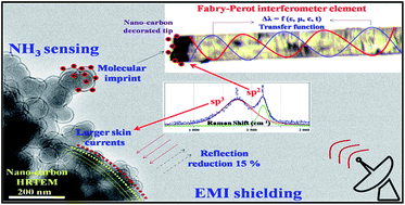
We report on the preparation and characterization of nano-carbon for applications in NH3 sensing and electromagnetic interference shielding (EMI, X-band, 8–12 GHz). Nano-carbon was synthesized by combustion of 1,7,7-trimethyl-bi-cycloheptan (camphor, C10H16O) deposited at 77 K. Morphological analysis showed nano-carbon was spherically concentric shells (40–50 nm); interconnected spatially. In Raman, vibration modes observed at 1390 (D) and 1580 (G) cm−1, indicated presence of sp3 within sp2 shells. UV-visible and photoluminescence spectroscopic analysis revealed that, band gap of nano-carbon was 4.5 eV with midgap of 2.7 eV and two flouro-excited states; making it useful for Fabry–Perot interferometer optical fibre gas sensor. Details of sensor system, its mechanism and transfer function analysis is presented. The system sensitivity was 3 ppm with response and recovery time, respectively, 5 and 8 s. The molecular imprint of NH3 on nano-carbon (1–5 ppb C-loss/10 cycles; 2[thin space (1/6-em)]:[thin space (1/6-em)]1, sp3[thin space (1/6-em)]:[thin space (1/6-em)]sp2 rupture) was obtained that set life time of sensor probe. In EMI, % reflection of nano-carbon was comparable with copper. The losses due to hopping and migration current were large in nano-carbon and attributed to in-plane σ-bond and tetrahedral sites in nano-carbon that interacted with radiation at higher skin depth, around four times more than that of copper. Details of EMI shielding mechanism is presented.


A Introduction

The search for multifunctional materials, especially for gas sensing and electromagnetic interference (EMI) shielding, is of great importance in the military and civil domains. In recent years, nano-carbon such as carbon nanotubes, reduced graphene oxide, and graphene have become popular sensing probes for gas detection,1 particularly for ammonia (NH3). It has been reported that nano-carbon showed good NH3 sensitivity due to unique structure e.g., small size, large specific surface area,2 and outstanding electronic properties such as high electron mobility,3 sensitivity to electrical perturbations through NH3 molecules. Hu et al. demonstrated NH3 gas sensor based on reduced graphene oxide, at room temperature.4 Cui et al. developed silver nanocrystal incorporated carbon nanotubes for NH3 sensors at room temperature.5 Ghosh et al. found NH3 sensitivity in the range of 200 to 2800 ppm, for reduced graphene oxide sensor probe.6 Mao et al. reviewed sensor study, focused on challenges and opportunities of nano-carbon based materials for gas detection.7 Further, the importance of EMI shielding has increased greatly as today's fast developing society is more dependent on electronics and growth of radio frequency radiation sources. The electromagnetic radiation, particularly, that at microwave frequencies tend to interfere with radars and electronics. Such interference is assumed to be strategically adverse in defence and, moreover, is hazardous in civil sector.8 Cao et al. has studied temperature dependence of permittivity of ultrathin graphene composites9 and multi-region microwave absorption of nanoneedle-like ZnO.10 In another study, He et al. reported tuneable electromagnetic attenuation capability of magnetic nanoparticles decorated reduced graphene oxides in microwave region.11 Wen et al. found the thinnest and most light weight materials with highly efficient microwave attenuation performance of reduced graphene oxide.12 In most of these studies, the emphasis is on graphene based nano-carbon material correlating dielectric, EMI shielding, and microwave-absorption performance.13,14

The another class of carbon is the amorphous nano-carbon, the broad name used for soot of the carbonaceous element. It is primarily composed of nano-carbon in the form of agglomerated nano-particles with diameter of about 10–50 nm. They have neither graphite nor diamond like phase of carbon15 and lead to interesting physical properties. Their degree of sp2 graphitic ordering ranges from nano-crystalline graphite to glassy carbon. One can define diamond like carbon as amorphous carbon which can have mixture of sp3 and sp2 sites with composition depending upon formation of amorphous phase. The basic element which makes this material interesting is their bond molecular environment that consists of σ and π states. They have significantly different behaviour and properties changes dramatically with composition of sp2 and sp3. Such nano-carbon is light weight, easy to synthesize, cost effective, stable at high temperature, and ecofriendly. The focus of the present work is to evaluate performance of such nano-carbon, obtained by pyrolysis of camphor at low temperature, for NH3 gas sensing and EMI shielding applications. The fabricated nano-particles consisted of sp2 + sp3 carbon having bond disorder in terms of unsaturated dangling bonds, vacancy mediated defects, etc. The nano-carbons were integrated with optical fibre based gas sensor. The performance characteristic of the designed sensor was investigated for full scale detection, response function and limit of detection. The evaluation of nano-carbon for EMI shielding was demonstrated by analysing dielectric function, dc and ac conductivity, skin depth and % reflection. Details are presented.

B Results and discussion

a Morphological analysis

Fig. 1 shows typical (a) HRTEM and (b) FESEM image of nano-carbon. The obtained structures are spherical shaped coagulated nano-carbon. It shows nature of deposited amorphous carbon soot in the form of spheres of dimension around 40–50 nm. The HR imaging revealed that, the nano-carbon consisted of concentric shells. At several sites, shell discontinuity and formation of amorphous zone was seen. Especially, at the outermost shell, the degree of amorphization seems to be more prominent. At some sites, we have seen highly crystalline outer shells detached from the core of nano-carbon. The two regions seem to be separated by un-crystalline carbon zones. In most of the cases, crystallinity was prominently observed in nano-carbon. Though, TEM gives two dimensional imaging, it seems that nano-carbon was interconnected. The SEM results resemble with TEM findings. The coagulated and connected nano-particles were clearly visible as seen in Fig. 1(b). The nano-carbon has formed three dimensional structures with homogeneous particle size distribution. A large number of HRTEM and FESEM micrographs were recorded and provided in ESI. Further, the obtained nano-carbon was in powder form can be easily be transformed into a coating on a desired substrate. Such high surface area, spatial, homogeneous and mix phased nano-carbon structure looks to be advantageous for molecular sensing, radiation shielding, etc.
image file: c6ra17422a-f1.tif
Fig. 1 Recorded images (a) HRTEM and (b) FESEM of nano-carbon.

The great versatility of nano-carbon arises from the strong dependence of their physical properties on the proportion/ratio of sp2 and sp3 bonds. Raman spectrum fundamentally depends on ordering of sp2 sites and indirectly on sp3 content.

b Raman studies

Raman scattering is unique tool to probe sp2 and sp3 fraction. In this section, brief Raman spectroscopic analysis of nano-carbon is presented in light of morphological analysis.16–18

Fig. 2(a) shows recorded spectrum of free standing nano-carbon. It consisted of two peaks, D and G. Broadly, they were, respectively, assigned to sp3 and sp2 phases of nano-carbon. The emergence of these phases is peculiar characteristic of amorphous carbon and indicative of large disorder. To determine this, a curve fitting was carried out in terms of spectroscopic parameters such as peak position, peak width, lineshape (i.e. Gaussian, Lorentzian or a mixture of both) and band intensity. The result of this line decomposition is indicated in Fig. 2. Several fits were tried leaving all spectroscopic parameters free to progress and the best fitting was invariably obtained for our spectrum. The D-peak was deconvoluted for three component namely D1 at 1392.77, D3 at 1534.12, and D4 at 1181.54 cm−1. Among them, D1 and D4 were Gaussian and D3 narrow Lorentzian. The D4 is superimposed molecular vibrations of sp2 + sp3 bonds,19 D1 tetrahedral carbon and D3 amorphous graphitic phase.20,21 The sp2 carbon attached to sp3 have vibrational features at frequencies less than 1500 cm−1. Similarly, for G-band curve fitting is shown. It consisted of narrow line width feature at 1605.59 cm−1 (G) and broad one at 1726.2 cm−1 (D2) assigned to breathing mode of nano-carbon shell. The result of this fitting was in good agreement with the literature work.22 It is interesting to note that, G mode was close to the main E22g band of crystalline graphite. This is further evidence in favour of rich sp2 crystalline environment in nano-carbon supported by narrower line width of G compared to D-band.19,25 Intensity of G-band was higher than that of D-band. It has dependence between the integrated intensity ratio ID/IG (1.5) which is inversely proportional to nano-crystalline planar size La ∼ 3 nm.17,23


image file: c6ra17422a-f2.tif
Fig. 2 Recorded Raman spectra for (a) nano-carbon powder, (b) nano-carbon deposited on copper. Inset shows vibration modes of metallic copper. Arrows indicate changes in vibration modes of copper by nano-carbon (λ ∼ 457 nm).

Fig. 2(b) is Raman spectrum recorded for nano-carbon deposited on copper. The Raman finger print modes of copper ∼200 and 500 cm−1 seems to be suppressed heavily while catalyzing nano-carbon. For such nano-carbon system, the ID/IG ratio was 2.3 with La ∼ 2 nm. This indicated that, amount of graphitization in nano-carbon changed when deposited on condensed copper (77 K). Perhaps La was incrementally enhanced in free standing nano-carbon. However, vibration modes of copper seem to be interacting with modes of nano-carbon. Interestingly, sp3 sites have only σ states, while sp2 sites also possess π states. They have implication on optical band structure in terms of occupancy, total energy, charge density and polarizability to generate optically active photo-excited states.

c Optical spectroscopy: band structure of nano-carbon

In the present work, we have demonstrated applications of the obtained nano-carbon for optical based gas sensing and EMI shielding. To utilize nano-carbon for optical applications, one need to know optical band gap and available photo-excited state of the material. UV-visible spectroscopy along with PL provides information about band gap and excited states. Fig. 3 shows recorded UV-visible spectrum of fabricated nano-carbon in non-aqueous medium. Plot (a) shows variation in normalized absorbance (α) as a function of wavelength (in nm). It showed a sharp peak centred ∼207 nm and a broad shoulder extended from 225–400 nm.
image file: c6ra17422a-f3.tif
Fig. 3 Recorded UV-vis absorption spectra of nano-carbon colloidal. Plot (a) absorbance (α) vs. wavelength and (b) (αhν)2 vs. energy. The dotted lines indicate tangent to Tauc curve.

The sharp peak was finger print of π–σ transition and broad feature was associated with π–π* transitions in nano-carbon. The plot (b) is Tauc graph showing (αhν)2 vs. energy. The extrapolation of straight line to (αhν)2 = 0 axis gives the value of band gap.24 The constructed tangents (red dotted lines) to the curve indicated respective optical band gap for π–σ and π–π* electronic environments. The bandgap of the nano-structure was 4.5 eV having midgap of 2.8 eV. Interestingly, the optical charge carriers have midgap state which were non-radiative in nature and having photo carrier excited states.25

Fig. 4(a) shows PL emission having two excited states one at 2.27 and other 1.6 eV. It showed that, nano-carbon consisted of two photo-excited states lower than midgap state. Thus, nano-carbon also possesses non-radiative fluoro-excited states. The fluoro-excited states were contributions from the dangling edges of sp2 + sp3 hetero-structures. In nano-carbon case the lower unoccupied molecular orbital (LUMO) band consisted of both s and p orbitals, contain a total number of eight electrons per Brillouin zone.26 The band scheme is shown in Fig. 4(b). By and large analysis revealed that, several states existed within HOMO–LUMO gap. These states have the wide dispersion of oscillator strength especially active in infrared and mid infrared region. This makes nano-carbon useful for optical based applications.27


image file: c6ra17422a-f4.tif
Fig. 4 (a) PL spectrum recorded for nano-carbon at excitation wavelength of λ ∼ 300 nm, (b) optical band scheme of nano-carbon.

d Sensor characteristic of nano-carbon

To utility, nano-carbon specimen was deposited on optical fibre used for gas sensing application. The schematic representation of Fabry–Perot interferometer optical fibre NH3 gas sensor is shown in Fig. 5.
image file: c6ra17422a-f5.tif
Fig. 5 Elements of Fabry–Perot interferometer optical fiber gas sensor set up consisted of SMF-28, 3 dB coupler, OSA, gas sensing chamber, and PC control unit. The photograph of zoomed portion of sensor probe is shown with schematics of NH3 molecule sensing.

In this set up, the incident mid-infrared radiation (wavelength 1510–1590 nm) from the source gets bifurcated from 3 dB coupler into the ratio of 50[thin space (1/6-em)]:[thin space (1/6-em)]50. The 50% of light travels through SMF-28 whose one end was perfectly cleaved normal to the fibre axis. The light from the fibre end reflects back giving rise to interference pattern. Thus, the cleaved fibre end was extremely sensitive to the reflection of light. In Fig. 5, zoomed portion of the fibre tip decorated with nano-carbon is shown in schematics. On interaction with NH3 molecules, the optical band gap of the tip coating changes with change in an the interference pattern. The remaining 50% radiation passes through OSA and was coupled to PC control unit that displayed sensing output for power and wavelength shift, as seen in Fig. 6.


image file: c6ra17422a-f6.tif
Fig. 6 Sensing response of nano-carbon tip to NH3 molecules, for a period of 180 s, at molecular concentrations ranging from 3–3000 ppm.

Initially, the spectrum was recorded for the tip in absence of NH3. Following this, 3 ppm of NH3 insufflate into gas chamber and onset, spectrum was recorded. The process iterated from 3–3000 ppm and at each iteration the response/recovery was monitored and recorded. It has been observed that, with subsequent increment in ppm level there was a shift in the wavelength. The sensing measurements were carried at room temperature and reliability as well as reproducibility in the sensor response has been noted well.

In Fig. 7(a) wavelength shift (Δλ) as function of molar concentration (C in ppm) of NH3 is plotted for various probe/gas interaction time, 60–180 s. At 3000 ppm, the sensor showed the wavelength shift of 1.66 nm for 180 s. For 3 ppm of gas, the wavelength shift of 80 pm was observed for 180 s. It has been observed that, as the NH3 concentration increases from 0 to 3000 ppm, the sensor showed prominent wavelength shift. All measurements were perfectly reproducible.


image file: c6ra17422a-f7.tif
Fig. 7 (a) Response function characteristics of wavelength shift (Δλ) with molar concentration (C in ppm) for different time period, and (b) functional response of the sensor in terms of (Δλ) and time at different ppm levels.
(i) Sensor transfer function. Transfer function of a sensor system quantifies response of stimuli as a function of input. The nature of ΔλC has been simulated for the measured time interval in the form of transfer function characteristics. At smaller time intervals i.e. upto 60 s, the function took simple form Δλ = K[thin space (1/6-em)]eC/M, where, M is interaction volume, K is sensitivity constant expressed as the product of molecular interaction length and molar concentration (C). In this time domain, the simulated curve parameters, indicated that the change in wavelength was of the order of 0.8–1.0 nm affecting 1000–1500 carbon molecules. The sensitivity for molecular NH3 was ∼7–8 atomic distances of carbon. For higher temporal domain, the statistical interaction scenario between NH3/nano-carbon system became more complex. This was particularly due to other physical component that started dominating the interaction such as diffusion of NH3 in sub-surface region of individual nano-carbon, mutual chemical potential (μ) and physisorption potential (ε) experienced by NH3/carbon ensemble, onset, within interaction volume, mismatch in the molecular vibration, etc. More diffusivity of NH3 increased the number of carbon atom that were participating in interaction, in this time domain, which was estimated ∼5000–6000. This had implication on both sensitivity and molar length in which sensitivity improved marginally to 10–15 molar length. For still higher sensing time, the ΔλC transfer function took the form: image file: c6ra17422a-t1.tif, in which molar interaction went in the order of 103 to 104 and beyond. The transfer function characteristic discussed here is, strictly, at 300 K. Any departure from this value introduces adiabatic perturbative term of higher order which has potential dependence on thermodynamics of interacting system.28 Fig. 7(b) shows variation in Δλ as function of time for both response and recovery. The empirical analysis of the curve indicated that, it was composed of linear and impulse response function which is express as, image file: c6ra17422a-t2.tif, where, T is interaction time, B is diffusivity (cm2 s−1) of NH3 molecule, ε and μ, respectively, rate of change of physisorption and chemisorption potential. The response and recovery time of about 5 and 8 s were noted, respectively. Table 1 indicate performance characteristics of our sensor.
Table 1 Performance sheet of nano-carbon sensor system
Parameters Performance and range
Gas selectivity NH3 (assessed and evaluated)
Full scale detection (instrumental) 3–3000 ppm
Pulse rise time 5 s
Rise response Linear
Pulse decay time 8 s
Decay response Impulse
Limit of detection (intrinsic) 1–5 ppb per 10 cycles (irreversible)
Time 0–180 s
Molar transfer function image file: c6ra17422a-t3.tif
Temporal transfer function image file: c6ra17422a-t4.tif
Temperature range 300 ± 10 K


(ii) Sensing mechanism. The nano-carbon consisted of sp2 + sp3 phase of carbon in which sp3 phase was distributed in-homogeneously and isotropically. At the sp2 + sp3 interface the coordination number of carbon atom connecting two phases is in disproportionate and lead to one under coordinated electron. In addition, there were π–π* conjugated electrons in sp2 zone. Moreover, Raman analysis revealed vacancy mediated disorder in nano-carbon system. At the vacancy site, there was non-uniform electron sharing between three uncoordinated carbon atoms. The two charge deficient carbon played role of acceptor atoms, wherein, the third carbon as the donor. The under coordinated electrons, π–π* conjugated electrons, and vacancy sites acted as the photo-carriers that participated in optical excitation process. This results into the behaviour of nano-carbon as an n-type photoconductor. The molecular NH3 on interaction with nano-carbon, transiently, changed the midgap, fluoro-excited gap and, consequently, optical gap. In NH3, nitrogen that carries lone pair of electrons get attracted to the charge deficient carbon atom sites by van der Waal interactions. The hydrogen atom in NH3 physically adsorb at the interface of sp2 and sp3. Since, NH3/nano-carbon interaction was statistical in physico-chemical nature, depending upon the stereo-regular configuration of sp2 + sp3, there could be possibility of complete charge transfer. This will have indentation on molecular vibrations of nano-carbon, analyzed before. Interestingly, the variations has been observed in post NH3 sensed nano-carbon revealed by Raman spectroscopy.
(iii) Molecular imprint of NH3 on nano-carbon. In Fig. 8(b) there are significant changes in the post NH3 treated nano-carbon sensing probe when compared to free standing nano-carbon (plot (a)). Broadly, G-band was decreased and D-band was increased and broaden. The broadening of the band indicated reduction in crystallite size of nano-carbon. Moreover, G-peak was shifted from 1605.59 to 1597.9 cm−1, after NH3 sensing. The down-shifting of G line position was attributed to enhancement in bond-angle disorder at G sites.29 The peaks D4 and D3 were disappeared, whereas, D2 was practically vanished. This indicated that, sp2 + sp3 sites and zones related to amorphous carbon were altered. The submerging of D3 and D4 into D1 was indicative of increased in unsaturated dangling bond character in nano-carbon. Although, the sensing action of nano-carbon probe seems to be completely reversible, macroscopically, however, at molecular level the imprint of NH3/nano-carbon interaction is identified, clearly, by Raman spectroscopy. The sum of molecular contribution of amorphous carbon moieties i.e. D4 + D3 was of the order of 7 × 10³ which got sacrificed during sensing action. Whereas, from sp2 environment ∼3 × 10³ dangling carbon bonds were modified in sensing 3–3000 ppm of NH3 molecules, at the end of several cycles. The rupture at sp3 was nearly twice than at sp2. Though the cumulative data is shown at the end of the cycles, one can investigate the effect after individual cycle. The result suggested that, the disordered carbon in nano-shell forms interstitial defects leading to molecular imprints.22,29–31 Further, the absence of D2 showed degradation in crystallinity which form non-graphitic phase of nano-sized dimension having polycrystalline/amorphous carbon nature. This was reflected in reduction of La from 3 (free standing nano-carbon) to 1 nm (post NH3 treated). The change corresponds to a second maximum in the graphite vibrational density of states near the M point of the Brillouin zone boundary, which became prominent in small graphite crystallites, after NH3 treatment. This resulted into lack of a long range translation symmetry which lead to a breakdown of the k-momentum conservation rule.32,33
image file: c6ra17422a-f8.tif
Fig. 8 Recorded Raman spectrum of (a) nano-carbon decorated on optical fibre tip, (b) post NH3 sensing (λ ∼ 457 nm).

e Nano-carbon for shield technology

Shielding of an object from incoming electromagnetic radiation is important in both military and civil sectors. EMI shielding is achieved by reflection as well as absorption of electromagnetic radiation by a material, which thereby acts as a shield against penetration of radiation.
(i) Coating characteristic of nano-carbon on copper. Fig. 9(a) shows recorded SEM cross sectional view of nano-carbon film. The image showed thickness of nano-carbon ∼ 60 μm on ∼25 μm copper foil. The film was uniform, however, having columnar deposition inhomogeneities at certain places. In general, most of the film was continuous laterally and longitudinally. Also, at some places the peeling effect was observed. A typical micrograph is shown and others are provided in ESI. In order to see the elemental composition of deposited nano-carbon, energy dispersive X-ray analysis (EDAX) was carried out. Fig. 9(b) indicate peak associated with oxygen, carbon and copper. The inset table shows elemental composition. The high amount of oxygen ∼ 12 atomic% was attributed to the presence of native oxide layer on copper.
image file: c6ra17422a-f9.tif
Fig. 9 (a) FESEM cross-section view of nano-carbon film deposited onto copper, (b) recorded EDAX spectrum and inset in (b) shows elemental composition.
(ii) dc conductivity. The electromagnetic rays in X-band, particularly, interact with nano-carbon material in the form of various losses such as electric conduction, hysteresis and electron spin resonance. Since, nano-carbon is nonmagnetic in nature, eddy current and electron spin resonance are dominant effect in microwave absorption. In this work, we have not carried out any study on electron spin resonance. However, to quantify eddy current losses, electrical conductivity of nano-carbon was measured and compared with copper.

Reflection is the primary mechanism of EMI shielding which depends on conductivity, both ac and dc, of shielding material. EMI shielding depends on the interaction between mobile charge carriers (electrons or holes) of the material and the electromagnetic field. The shielding material with good electrical conductivity is necessary requirement in shield technology. Specifically, reflection loss is the function of ratio of σr/μr, where, σr, electrical conductivity relative to copper and, μr, relative magnetic permeability.34

Fig. 10 shows measured IV characteristic of nano-carbon compared with copper. The conductivity was estimated using: image file: c6ra17422a-t5.tif, where, l, is length of active channel, m, slope, h, thickness and, w, width of conducting channel. Table 2 shows IV measurement parameters estimated for both the systems.


image file: c6ra17422a-f10.tif
Fig. 10 Measured current–voltage (IV) characteristic of nano-carbon and copper foil. Inset shows typical photograph of samples with electrical connections and contact developed.
Table 2 IV measurement parameters for copper and nano-carbon
Parameters Copper Nano-carbon
Slope (m) 0.16013 0.90712
Thickness (h) 25 μm 60 μm
Width (w) 2 cm 2 cm
Length (l) 2 cm 2 cm
dc conductivity (σdc) 2.5 × 10⁵ s m−1 1.8 × 10⁴ s m−1
Skin depth (δ) 11 nm 42 nm


(iii) % reflection analysis. Fig. 11 shows % reflection data obtained for copper and nano-carbon, in X-band regime. The amount of reflection from nano-carbon was recorded to be ∼85%, comparable to copper (95%). For EMI shielding material, the reflection, including reflection from surface and interface scattering, will increase with increasing conductivity of the materials.
image file: c6ra17422a-f11.tif
Fig. 11 Recorded % reflection for both the systems, in X-band.

Further, from Table 2, the magnitude of σdc for copper was ∼10 times high compared to nano-carbon. Another important estimated parameter is skin depth, δ, the extent to which incident radiation interacted with material and given by: image file: c6ra17422a-t6.tif, where f, applied frequency, μ = 1 (for copper). For 10 GHz, the value of δ was ∼10 and ∼40 nm for copper and nano-carbon, respectively. In both, copper and nano-carbon, reflection loss caused due to eddy current was more due to skin effect.35,36

Fig. 12 shows imaginary permittivity, ε′′ of copper and nano-carbon. Reflection loss of microwave radiation is mainly due to impedance matching condition and the change of electromagnetic parameters of complex permittivity.37 Free electrons plays important role in imaginary part of complex permittivity due to good electrical conductivity.34,38,39 According to the free electric theory,40 ε′′ could therefore be obtained by using: image file: c6ra17422a-t7.tif. The relation showed that, σac plays the dominating role in ε′′. It seems that, the σac of copper was marginally high compared to nano-carbon. This change was due to bond environment of copper and nano-carbon medium.


image file: c6ra17422a-f12.tif
Fig. 12 Recorded imaginary permittivity, ε′′, as a function of frequencies, exhibiting monotonic relationship between frequency and ε′′.
(iv) Shielding mechanism. The scheme of interaction mechanism of incident electromagnetic radiation with nano-carbon and copper medium is shown in Fig. 13. In copper, the conduction mechanism is due to free mobile charge carriers. While in nano-carbon there exist both migrating conduction and hopping conduction due to hetero-structure sp2 + sp3 carbon zones.37,41–43 Thus, increasing total conductivity in disordered spherical amorphous nano-carbon concentric shells enhances imaginary permittivity ε′′ resulting in more reflection, comparable to copper. However, incident radiation of ∼15% is attenuated within the nano-carbon layer due to larger penetration depth of electromagnetic radiation in nano-carbon compared to copper. On interaction the incident electric field component gets coupled strongly with the molecular electric field of sp2 σ-bond. This resulted into larger dissipation of field into heat in nano-carbon.
image file: c6ra17422a-f13.tif
Fig. 13 Schematic illustration showing electromagnetic wave interaction of nano-carbon and copper with differing skin depth level, in X-band.

Thus, comparative microwave reflection property of nano-carbon with copper, particularly in X band region, is advantageous. Copper being metal is high density, corrosion prone, and expensive material for shielding technology. On the other hand, nano-carbon is light in weight, ecofriendly, stable at high temperature, easy to synthesize and cost effective. Thus, nano-carbon is well suited candidate for EMI shielding over copper.

C Experimental

a Sample preparation: low temperature nano-carbon thin film deposition

Fig. 14 shows scheme of nano-carbon deposition at low temperature. The commercially available 1,7,7-trimethyl-bi-cycloheptan (C10H16O, camphor) of analytical grade was taken as the starting material to grow nano-carbon films. The deposition was carried out at 77 K under normal thermodynamic conditions. In order to deposit nano-carbon onto copper, initially, a rectangular shaped boat of dimension 5 × 3 × 1 cm3 has been prepared from copper (thickness ∼ 25 μm, purity ∼ 99.8%, Alfa Aesar) and subjected to sonication. Sonication was carried out at a constant frequency of 30 kHz with power of 50 mW. The boat was immersed into methanol for cleaning and kept in water bath for a period of 15 min, for sonication at room temperature. Following this, drying process, using an IR heating lamp (power 500 W), was carried out for a period of 1 h. For deposition process, stainless steel spatula mounted on a fixed platform and prior to deposition, starting material was kept on the rectangular side of spatula. The platform was vertically moveable clamp coupled to a stand. The arrangement was such that clamp can move freely in vertical direction so that its open end can be brought in the vicinity of spatula end. This facilitates to enhance yield of nano-carbon on substrate by adjusting vertical distance between clamp and spatula mount. The boat was poured with liquid nitrogen. After camphor loading on specula, boat was clamped and brought in vicinity of precursor pellet that has been subjected to combustion for deposition. Once deposition was over, the base of boat on which thin film deposited cut into the dimensions of 2.5 × 1.5 cm2 for assessment of deposited nano-carbon.
image file: c6ra17422a-f14.tif
Fig. 14 Scheme of nano-carbon deposition at low temperature.

b Characterizations

The deposited nano-carbon specimen was gently scrubbed from the substrate using razor blade and collected into a polyethylene tetra phetelite vyal. These samples were subjected to electron microscopy, Raman, UV-visible, photoluminescence (PL) spectroscopy.
(i) Morphological investigations using electron microscopy. In order to investigate morphology of nano-carbon, high resolution transmission electron microscopy (HRTEM, G220S-Twin, Tecnai, FEI, USA) measurements were performed, using beam potential of 300 kV. For this propose, some amount of nano-carbon was immersed into isopropyl alcohol (IPA) subjected to sonication for a period of 15–20 min. Using a micropipette, ∼10 μl suspension was released onto a standard carbon coated copper grid. The prepared grids were allowed to dry in a closed environment. After a period of 24 h, they underwent HRTEM measurement at base pressure ∼ 10−11 Torr. A large number of images were taken in order to quantify structure, dimension and other details. In another study, surface morphology of nano-carbon was investigated using a field emission scanning electron microscopy (FESEM; Zeiss Sigma), at beam potential of 5 kV. For measurements, no gold coating was employed prior to imaging. Moreover, interface morphology of nano-carbon deposited on copper was investigated.
(ii) Raman spectroscopy. Vibration spectroscopy measurements of nano-carbon, deposited nano-carbon and copper substrates were carried out using Raman spectroscopy (LABRAM HR-800). Prior to measurements, calibration of the system was carried out using silicon substrate at 457 nm excitation wavelength. The beam energy was ∼1 mW at the sample surface. The measurements was performed over the wavenumber range of 200–3000 cm−1, at room temperature. The resolution of the system was 4 cm−1. To confirm reproducibility of measured spectrum, several sites were examined for nano-carbon. For quantitative analysis, all spectra underwent several chemo-metric spectral manipulation techniques, using Labspecs 5.0 software, Horiba Industries Corporation, lesulis, France. Raleigh and florescence induced background scattering were best fitted for 4th order polynomial baseline and eliminated form all spectra prior to peak fitting.
(iii) UV-visible spectroscopy. For UV-visible spectroscopic measurements, nano-carbon powder was dispersed into IPA and sonicated for a period of 30 min. Following this, the suspension was immersed into spectrometer (Specord 210 PLUS, analytik jena) cuvette along with plane solution in another. The full range (200–800 nm) background spectrum was recorded and subtracted, followed by the measurements. The data of absorption (α) as function of wavelength was recorded. The absorption data was used for PL excitation.
(iv) PL spectroscopy. For PL (Ocean Optics DH-2000-BAL) measurements, similar methodology was adopted as described above. The data of PL intensity as a function of wavelength (200–1200 nm) was collected for nano-carbon.

c Measurements of NH3 gas sensing

The gas sensing set up (photograph shown in ESI, Fig. S4) consisted of a broadband source (Micron optics, Optical Sensing Analyzer (OSA) Si720) of wavelength (1510–1590 nm, with resolution of 0.25 pm) and power of 1 mW that launches light into single mode fibre (SMF-28) through 3 dB optical coupler. The light splits at coupler in ratio of 50[thin space (1/6-em)]:[thin space (1/6-em)]50, half portion goes towards the free end of coupler and remaining light travels towards the detector. The free distal end of Y-coupler fibre was perfectly cleaved using a cleaver. The reflected light gets coupled back into the detector giving rise to interference pattern. The free end of the fibre was coated with nano-carbon.

d EMI shielding measurements

To investigate shielding performance of nano-carbon, dc conductivity (σdc), and microwave scattering measurements were performed.
(i) dc conductivity (σdc). Using four probe technique σdc of copper and nano-carbon deposited films were determined. The data was acquired using a standard Keithley 2420 picoammeter/voltage source equipped with data acquisition software.
(ii) Microwave scattering parameters. X-Band (8–12 GHz, 25–37.5 mm) measurements were carried out for exploring microwave scattering properties of nano-carbon and copper. For this purpose, PNA network analyzer (Agilent, N5222A) was used having full range 10 MHz to 26.5 GHz. The instrument was equipped with wave guides of dimensions 2.3 × 1.1 cm2 for measuring S-parameters. Prior to experiments, VNA was started for 2 h for stabilizing the microwave source. Initially, full two port calibration of VNA was performed on the test specimen in order to avoid errors due to directivity, isolation, source, load match, etc. The calibration was performed in both forward and reversed direction. S11 parameter was determined from one port measured scattering data with the help of commercially available Agilent software module 85071, based on the procedure given in Agilent product note. The sample was mounted into quarterwave plate slot and measurements were performed. Set up is shown in Fig. S5, in ESI.

D Conclusions

The utility of nano-carbon for effective gas sensor and efficient EMI shielding applications have been demonstrated. The nano-carbon was obtained by combustion of camphor precursor. The material was assessed for structure–property relationship using HRTEM, FESEM, Raman (λ ∼ 547 nm), UV-visible, and PL spectroscopy. Morphological studies revealed that, structures were three dimensionally interconnected spherical nano-carbon. It consisted of both sp2 and sp3 phase in which sp3 was inhomogeneously distributed within nano-sphere, especially, at the surface. The integrated intensity ratio ID/IG, estimated using Raman, was found to be 1.5 for nano-carbon. Tauc plot analysis revealed that, optical band gap of nano-carbon was ∼4.6 eV with several photo-excited states making it useful for gas sensing application. The performance characteristics of sensor was studied, for wavelength shift with change in molecular concentration and time, at room temperature. Interaction of NH3/nano-carbon was statistically physico-chemical in nature. The stereo-regular configuration of sp2 + sp3 in terms of under coordinated-, π–π* conjugated-electrons, and vacancy sites made nano-carbon n-type photoconductor. On interaction, whose bandgap modifies, transiently. In Raman, contribution of sacrificed sp3 was ∼7 × 10³, whereas, for sp2 ∼3 × 10³ in sensing 3–3000 ppm NH3 molecules. The rupture of sp3 sites were twice than that of sp2. In EMI shielding utility parameters of nano-carbon was quantified by estimating σdc, ε′′, σac, δ, and % reflection derived from S-parameters. In analysis, σdc, for nano-carbon was ten times less than copper engaging incident radiation four times higher in skin of nano-carbon. On interacting with nano-carbon, component of incident electric field got coupled strongly to sp2 molecular field, especially, in-plane σ-bonds. Since, these were in-plane bonds, directed along carbon network, excitations of σ-electrons bridged to two carbon atoms accommodate interaction energy to dissipate within carbonaceous shells in the form of heat. The incident field was capable to rotate three atoms branched to central sp3 carbon. As a result, overall % reflection was 85% for nano-carbon which is comparable to copper (95%). This makes nano-carbon coating useful for radar shielding material in X-band. Our result showed multifunctional character of nano-carbon obtained by facile combustion of hydrocarbon precursor.

Acknowledgements

The authors at DIAT acknowledges Dr Surendra Pal, Vice Chancellor for support. Funding support of the “DIAT-DRDO Programme on Nanomaterial”, DRDO is gratefully acknowledged. We are also thankful to Bhaskar Rao for helping in performing VNA measurements.

References

  1. J. Kong, N. R. Franklin, C. Zhou, M. G. Chapline, S. Peng, K. Cho and H. Dai, Science, 2000, 287, 622–625 CrossRef CAS PubMed.
  2. A. Peigney, C. Laurent, E. Flahaut, R. R. Bacsa and A. Rousset, Carbon, 2001, 39, 507–514 CrossRef CAS.
  3. A. Javey, J. Guo, Q. Wang, M. Lundstrom and H. J. Dai, Nature, 2003, 424, 654–657 CrossRef CAS PubMed.
  4. N. Hu, Z. Yang, Y. Y. Wang, L. Zhang, Y. Y. Wang, X. Huang, H. Wei, L. Wei and Y. Zhang, Nanotechnology, 2014, 25, 025502 CrossRef PubMed.
  5. S. Cui, H. Pu, G. Lu, Z. Wen, E. C. Mattson, C. Hirschmugl, M. Gajdardziska-Josifovska, M. Weinert and J. Chen, ACS Appl. Mater. Interfaces, 2012, 4, 4898–4904 CAS.
  6. R. Ghosh, A. Midya, S. Santra, S. K. Ray and P. K. Guha, ACS Appl. Mater. Interfaces, 2013, 5, 7599–7603 CAS.
  7. S. Mao, G. Lu and J. Chen, J. Mater. Chem. A, 2014, 2, 5573–5579 CAS.
  8. N. Li, Y. Huang, F. Du, X. He, X. Lin, H. Gao, Y. Ma, F. Li, Y. Chen and P. C. Eklund, Nano Lett., 2006, 6, 1141–1145 CrossRef CAS PubMed.
  9. W.-Q. Cao, X.-X. Wang, J. Yuan, W. W. Z. Wang and M. Cao, J. Mater. Chem. C, 2015, 3, 10017–10022 RSC.
  10. J. Liu, W. Q. Cao, H. B. Jin, J. Yuan, D. Q. Zhang and M. S. Cao, J. Mater. Chem. C, 2015, 3, 4670–4677 RSC.
  11. J.-Z. He, X.-X. Wang, Y.-L. Zhang and M.-S. Cao, J. Mater. Chem. C, 2016, 4, 7130–7140 RSC.
  12. B. Wen, X. X. Wang, W. Q. Cao, H. L. Shi, M. M. Lu, G. Wang, H. B. Jin, W. Z. Wang, J. Yuan and M. S. Cao, Nanoscale, 2014, 6, 5754–5761 RSC.
  13. M. Lu, X. Wang, W. Cao and J. Yuan, Nanotechnology, 2016, 27, 65702 CrossRef PubMed.
  14. B. Wen, M. Cao, M. Lu, W. Cao, H. Shi, J. Liu, X. Wang, H. Jin, X. Fang, W. Wang and J. Yuan, Adv. Mater., 2014, 26, 3484–3489 CrossRef CAS PubMed.
  15. H. Darmstadt, C. Roy, S. Kaliaguine, G. Xu, M. Auger, A. Tuel and V. Ramaswamy, Carbon, 2000, 38, 1279–1287 CrossRef CAS.
  16. D. S. Knight and W. B. White, J. Mater. Res., 1989, 4, 385–393 CrossRef CAS.
  17. L. Nikiel and P. W. Jagodzinski, Carbon, 1993, 31, 1313–1317 CrossRef CAS.
  18. P. K. Bachmann and D. U. Wiechert, Diamond Relat. Mater., 1992, 1, 422–433 CrossRef CAS.
  19. B. Dippel, H. Jander and J. Heintzenberg, Phys. Chem. Chem. Phys., 1999, 1, 4707–4712 RSC.
  20. L. C. Nistor, J. Van Landuyt, V. G. Ralchenko, T. V. Kononenko, E. D. Obraztsova and V. E. Strelnitsky, Appl. Phys. A: Solids Surf., 1994, 58, 137–144 CrossRef.
  21. L. H. Robins, E. N. Farabaugh and A. Feldman, J. Mater. Res., 2011, 5, 2456–2468 CrossRef.
  22. T. Jawhari, A. Roid and J. Casado, Carbon, 1995, 33, 1561–1565 CrossRef CAS.
  23. F. Tuinstra and L. Koenig, J. Chem. Phys., 1970, 53, 1126–1130 CrossRef CAS.
  24. J. Tauc, Amorphous and Liquid Semiconductors, Springer Science & Business Media, 2012, vol. 27 Search PubMed.
  25. V. L. Bonch-Bruevinch, The Optical Properties of Solids, Academic Press, New York and London, 1966, vol. 34 Search PubMed.
  26. J. Robertson and E. O'Reilly, Phys. Rev. B: Condens. Matter Mater. Phys., 1987, 35, 2946–2957 CrossRef CAS.
  27. W. A. Harrison, Phys. Rev. B: Solid State, 1973, 8, 4487–4498 CrossRef CAS.
  28. E. Llobet, Sens. Actuators, B, 2013, 179, 32–45 CrossRef CAS.
  29. R. O. Dillon, J. A. Woollam and V. Katkanant, Phys. Rev. B: Condens. Matter Mater. Phys., 1984, 29, 3482–3489 CrossRef CAS.
  30. J. D. Pasteris, Appl. Spectrosc., 1989, 43, 567–570 CrossRef CAS.
  31. J. N. Rouzaud, A. Oberlin and C. Beny-Bassez, Thin Solid Films, 1983, 105, 75–96 CrossRef CAS.
  32. R. J. Nemanich and S. A. Solin, Phys. Rev. B: Condens. Matter Mater. Phys., 1979, 20, 392–401 CrossRef CAS.
  33. G. Dresselhaus and M. Dresselhaus, Topics in applied physics: light scattering in solids III, Springer Verlag, Berlin, 1982, vol. 51 Search PubMed.
  34. D. D. L. Chung, Carbon, 2001, 39, 279–285 CrossRef CAS.
  35. N. Idir, Y. Weens and J. J. Franchaud, IEEE Trans. Dielectr. Electr. Insul., 2009, 16, 147–154 CrossRef.
  36. S. H. Liu, J. M. Liu and X. L. Dong, Electromagnetic interference shielding and microwave absorption materials, Chemical Industrial Press, 2007 Search PubMed.
  37. M. S. Cao, W. L. Song, Z. L. Hou, B. Wen and J. Yuan, Carbon, 2010, 48, 788–796 CrossRef CAS.
  38. J. Wu and D. D. Chung, Carbon, 2002, 40, 445–447 CrossRef CAS.
  39. B. Wen, M. S. Cao, Z. L. Hou, W. L. Song, L. Zhang, M. M. Lu, H. B. Jin, X. Y. Fang, W. Z. Wang and J. Yuan, Carbon, 2013, 65, 124–139 CrossRef CAS.
  40. S. Ramo, J. R. Whinnery and T. Van Duzer, Fields and waves in communication electronics, John Wiley and Sons, New York, 1984 Search PubMed.
  41. M.-S. Cao, X.-X. Wang, W.-Q. Cao and J. Yuan, J. Mater. Chem. C, 2015, 3, 6589–6599 RSC.
  42. M.-M. Lu, W.-Q. Cao, H.-L. Shi, X.-Y. Fang, J. Yang, Z.-L. Hou, H.-B. Jin, W.-Z. Wang, J. Yuan and M.-S. Cao, J. Mater. Chem. A, 2014, 2, 10540 CAS.
  43. H. Yang, M. Cao, Y. Li, H. Shi, Z. Hou, X. Fang, H. Jin, W. Wang and J. Yuan, Adv. Opt. Mater., 2014, 2, 214–219 CrossRef.

Footnote

Electronic supplementary information (ESI) available: Details of electron microscopy images. See DOI: 10.1039/c6ra17422a

This journal is © The Royal Society of Chemistry 2016
Click here to see how this site uses Cookies. View our privacy policy here.