
Sub-diffraction demagnification imaging lithography by hyperlens with plasmonic reflector layer
Ling Liu,
Kaipeng Liu,
Zeyu Zhao,
Changtao Wang,
Ping Gao and
Xiangang Luo*
State Key Laboratory of Optical Technologies on Nano-Fabrication and Micro-Engineering, Institute of Optics and Electronics, Chinese Academy of Science, P.O. Box 350, Chengdu 610209, China. E-mail: lxg@ioe.ac.cn
First published on 26th September 2016
Abstract
In recent years, hyperlens technology has attracted more attention because of its function of magnification and demagnification. In this study, hyperlens demagnification imaging lithography was experimentally demonstrated with sub-diffraction resolution of about 55 nm line width and about 1.8 demagnification factor at 365 nm. The hyperlens was composed of multiple Ag/SiO2 films and combined with a resist layer and a plasmonic Ag reflector. It was employed to project mask patterns to subwavelength images for nanolithography. It was found that the plasmonic reflector contributes remarkably to improving imaging contrast, fidelity and efficiency by inhibiting the negative influences from the radial electric field components in the resist region. Furthermore, discussions about imaging influences with geometrical parameters are also presented.
Introduction
The resolution of conventional optical imaging lithography is restricted by the diffraction limit to approximately half of the light wavelength in the medium due to the absence of evanescent waves carrying subwavelength information. In 2000, the concept of a perfect lens with negative refraction index material was proposed for amplifying evanescent waves and realizing perfect imaging with unlimited resolution in the ideal case.1 Resembling such a perfect lens, a superlens, composed of a metal film with matched negative permittivity, was found to successfully amplify evanescent waves by the excitation of surface plasmon polaritons, resulting in sub-diffraction limit resolution imaging as well. Since then, many types of super resolution lenses and methods have been investigated both computationally and experimentally.2–16Sub-diffraction optical imaging lithography is one important application that has been investigated extensively with various plasmonic lenses, including smooth superlens,4 reflective plasmonic lens17 and plasmonic cavity lens,18 etc., demonstrating sub-diffraction lithography with resolution below 22 nm,18 high aspect ratio19 and the ability to go beyond the conventional near field diffraction limit.20 Unfortunately, the imaging performances of the abovementioned methods are confined to the near field region and feature a zoom factor of just 1![[thin space (1/6-em)]](https://www.rsc.org/images/entities/char_2009.gif) :1. As one solution to this problem, hyperlenses have been proposed for far field imaging in a magnifying or demagnifying manner.21–23 A hyperlens usually consists of alternately stacked metal and dielectric films in concentric form and the object and image planes are positioned at the inner and outer most radius. Super resolution magnified images were observed with cylindrical and spherical hyperlenses24,25 and two dimensional hyperlenses were constructed on a planar film.26 Some methods were proposed for designing hyperlenses with flat images and/or object surfaces by coordinate transformations27–29 and artificial shape cutting.22
:1. As one solution to this problem, hyperlenses have been proposed for far field imaging in a magnifying or demagnifying manner.21–23 A hyperlens usually consists of alternately stacked metal and dielectric films in concentric form and the object and image planes are positioned at the inner and outer most radius. Super resolution magnified images were observed with cylindrical and spherical hyperlenses24,25 and two dimensional hyperlenses were constructed on a planar film.26 Some methods were proposed for designing hyperlenses with flat images and/or object surfaces by coordinate transformations27–29 and artificial shape cutting.22
In this study, we experimentally demonstrated a preliminary hyperlens for sub-diffraction demagnification imaging lithography. A plasmonic reflector layer (PRL) was combined with a hyperlens to obtain high contrast and good fidelity images by engineering electric field components in the photo resist area. The resist patterns with 55 nm line width and demagnification factor about 1.8 were successfully obtained in experiments with a 365 nm i-line mercury lamp.
Experimental
Fig. 1(a) shows the schematic of the designed hyperlens consisting of a mask pattern, cylindrical hyperlens with Ag and SiO2 films, photoresist layer and an Ag reflector. Presented in Fig. 1(b) is the process for the hyperlens fabrication and demagnification imaging lithography experiment. First, a V shape groove with 90 nm width and 200 nm depth was milled on a quartz substrate by Focused Ion Beam (FIB) and etched in buffered oxide etch (BOE) solution to get a nearly half cylindrical groove with a radius of 500 nm, width 800 nm and thickness 200 nm. For the convenience of fabricating multiple films and resist layers, the thickness was less than the radius with a large groove opening aperture. A 40 nm Cr film was deposited and milled by FIB into two slits with a 100 nm line width and 250 nm center to center distance. After that, a PMMA layer was spun on top and etched to about 45 nm thickness. Then, 15 layers of Ag and SiO2 films, each with 20 nm thickness, were alternately deposited. A layer of Ge with 1–2 nm thickness was pre-deposited beneath every Ag film as a wetting material to improve surface smoothness.30,31 The measured RMS roughness of the top Ag surface by AFM was 1.2 nm. Diluted SX AR-P3170 positive resist layer of about 50 nm thickness was spun onto the top Ag surface. The final step was to deposit a 120 nm thick Ag reflector upon the resist layer.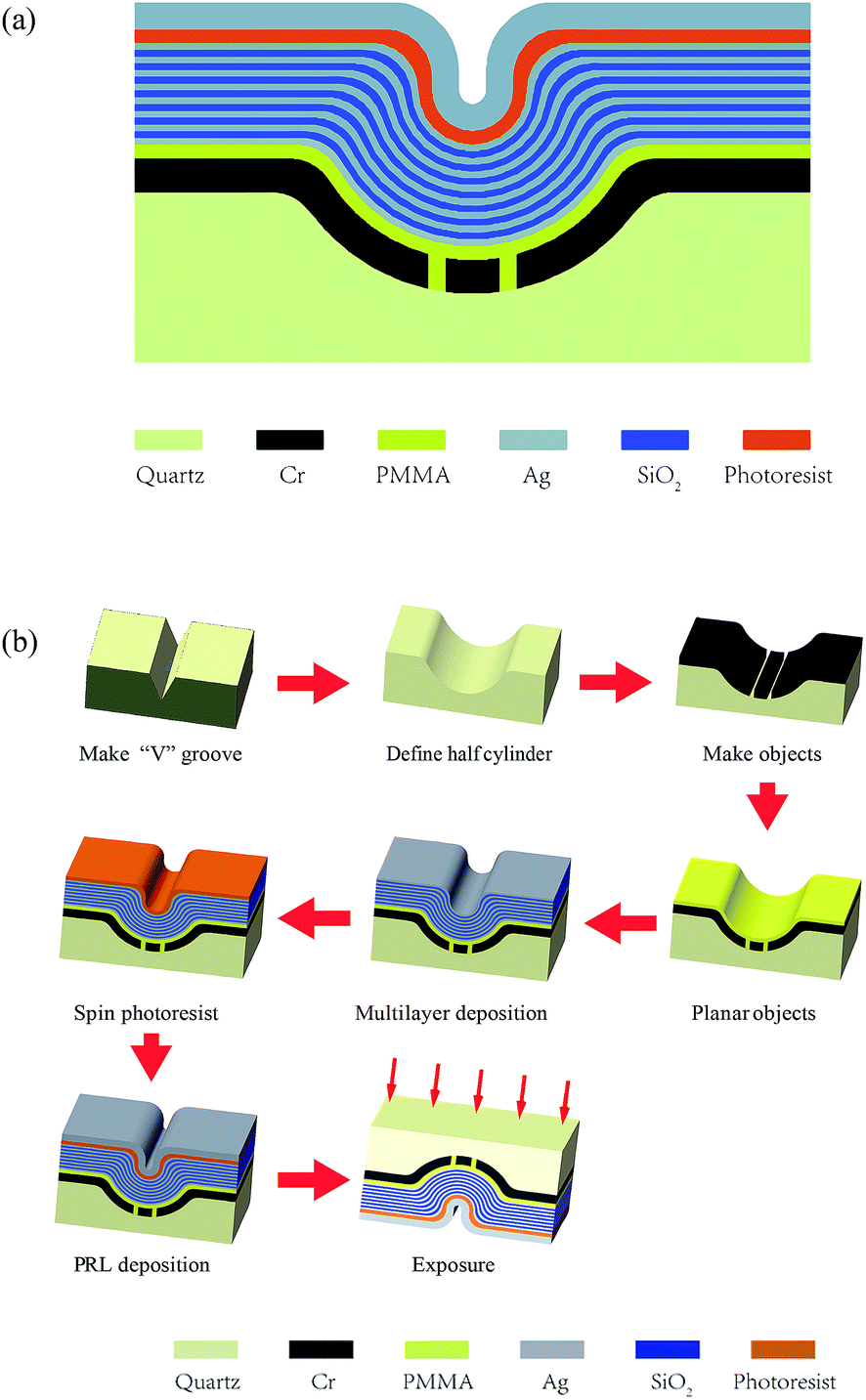 | ||
| Fig. 1 (a) Schematic of the hyperlens with plasmonic reflector layer. (b) Process flow of hyperlens fabrication and lithography. | ||
Fig. 2(a) shows the SEM image of the hyperlens structure in a cross sectional view. Fig. 2(b) is the SEM picture of a pair of transparent slit masks before being covered by the hyperlens, showing the 250 nm center-to-center distance and 100 nm line width. The sample with PRL was exposed from the bottom side of the quartz substrate by a filtered and nearly collimated mercury lamp illumination setup (central light wavelength 365 nm and 10 nm line width). After peeling off the PRL, the exposed hyperlens sample was developed at room temperature.
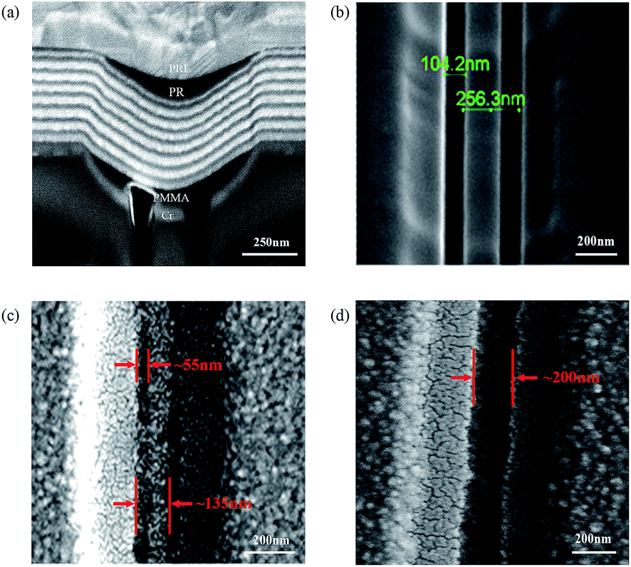 | ||
| Fig. 2 (a) SEM image of the cross section of hyperlens. (b) The two slits mask pattern with 100 nm line width at 250 nm center-to-center distance. (c) Lithography result of resist pattern with hyperlens and PRL with 55 nm line width at 135 nm pitch. (d) Resist pattern of hyperlens without PRL. | ||
The demagnification imaging lithography result with hyperlens accompanied by PRL is presented in Fig. 2(c), where two parallel lines could be clearly distinguished with a line width of ∼55 nm and a separation distance ∼135 nm (about 1/2.7 times that of the light wavelength), corresponding to demagnification ratio of ∼1.85 for the distance. As for the hyperlens without PRL, as shown in Fig. 2(d), the two slits could not be resolved and the image merged into one wide line resist pattern with a width of ∼200 nm.
Results and discussion
COMSOL Multiphysics software was used to simulate the imaging performance of the designed hyperlens and explain the experimental results. The permittivity of Cr, PMMA, Ag, and SiO2 at 365 nm light wavelength is εCr = −8.55 + 8.96i,4 εPMMA = 2.3, εAg = −2.3983 + 0.477i, εSiO2 = 2.2987 + 0.0054i, respectively. The normalized electric field intensity distribution of the hyperlens with and without PRL are shown in Fig. 3(a) and (b), respectively. As the light transmits through mask patterns and propagates inward along the radial direction of the hyperlens, angular wave vectors gradually increase and the sub-diffraction demagnified optical pattern is generated in the resist layer. Plotted in Fig. 3(c) is the image contrast of the two lines mask pattern for the observation positions ranging from 10 nm to 40 nm below the output surface. Herein, the intensity contrast of the images is defined as I = (|E|max2 − |E|min2)/(|E|max2 + |E|min2). It was found that, the image contrast of the hyperlens with PRL was considerably high, usually larger than 0.6 in the resist layer with 50 nm thickness. The hyperlens without PRL, however, showed much smaller contrast, even less than 0.4 at positions 30 nm and less from hyperlens, implying that no successful photo lithography could be realized in this case.19 This helps to explain why a resolved resist pattern was not observed in the lithography experiment shown in Fig. 2(d). | ||
| Fig. 3 Normalized electric field intensity distributions for hyperlens with PRL (a) and without PRL (b). (c) Variations of image contrast at positions 10 nm to 40 nm from hyperlens. The insets are the image profiles of the hyperlens with/without PRL, respectively. (d) Lateral positions relation between images and two silts on the mask with variant center to center distance. | ||
In addition, the PRL scheme helped to significantly enhance the electric intensity of the images, to about 4 times larger than that without PRL, as shown in the inset of Fig. 3(c). This was mainly due to the amplification of the evanescent waves and resonance effect in the plasmonic cavity lens composed of PRL and the outer most Ag film of the hyperlens. On the other hand, the positional relationship of the object plane and image plane for the configuration of the hyperlens with and without PRL is shown in Fig. 3(d), demonstrating that a more uniform demagnification ratio ∼2.05 could be obtained for the hyperlens with PRL. Moreover, the experimentally achieved demagnification ratio was about 1.85. This represents an acceptable difference between simulation and experiment. Moreover, the imperfect concentricity of the fabricated structure was responsible for the difference.
The difference of imaging performance between hyperlens with and without PRL could be further investigated by considering the imaging behaviors of the radial component |Er|2 and angular component |Eθ|2, as shown in Fig. 4.32 For the control case without PRL, the |Eθ|2 light distribution showed two slits in clearly resolved images, as shown in Fig. 4(a). As the intensity of |Eθ|2 was comparable with that of |Er|2, the greatly blurred image profile of |Er|2 would not deliver an acceptable image in the measure of |Eθ|2 + |Er|2, as demonstrated in Fig. 3(b) and in the experimental results in Fig. 2(d). Fortunately, the introduction of cavity modes between the hyperlens and PRL helped to greatly enhance the component |Eθ|2 and inhibit |Er|2 at the same time. Herein, the calculated intensity of |Eθ|2 is about 20 times than that of |Er|2 in the image area for the hyperlens with PRL (Fig. 4(b)). Thus, no evident image degradation was observed, even though the |Er|2 profile deviates from expected image distribution, resulting in imaging with high contrast and fidelity in the lithography experiment (Fig. 3(a)).
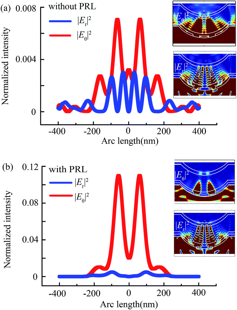 | ||
| Fig. 4 (a) Plots of normalized image intensity distributions for radial component |Er|2 and angular component |Eθ|2 at 30 nm away from hyperlens without PRL. (b) is same as (a) but the hyperlens is configured with PRL. All insets in (a) and (b) are the corresponding light distributions of hyperlens imaging. | ||
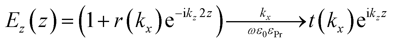
For simplicity, the planar counterpart of the plasmonic cavity structure consisting of the Ag film lens/photoresist/Ag reflector was further used for analysing different performances of the two types of electrical field components. When light modes propagate into the plasmonic cavity, multiple reflections between the two Ag films occur inside the cavity.33 Considering that the Ag reflector was thick enough and evanescent waves inside the photoresist decayed quickly in the multiple reflection process, the single reflection is assumed to dominate the imaging process in the photoresist layer. The components of the electrical field in the photoresist layer could be approximately expressed as:34
 | (1) |
 | (2) |
 | ||
| Fig. 5 The electrical field amplitude (a) |Ex| and (b) |Ez| as functions of the transverse wavevector kx/k0 with and without Ag reflector. | ||
The thickness of the Ag film lens, photoresist and Ag reflector were 20 nm, 50 nm and 120 nm, respectively. From Fig. 5(a) and (b), it can be seen that the Ag reflection layer beneath the photoresist layer significantly enhanced the |Ex|, whereas |Ez| was effectively suppressed simultaneously. As a result, the ratio between |Ex| and |Ez| could be well modulated in the plasmonic cavity structure to inhibit the negative contribution to enhance the imaging contrast in the measure of |Ex|2 + |Ez|2.
The electrical field angular component |Eθ|2 and radial component |Er|2 in Fig. 6(a) and (b) were obtained in simulation of the curved hyperlens with PRL. The observed plane was 20 nm away from the hyperlens. In Fig. 6(a), the two obvious resolved peaks of |Eθ|2 could always be seen regardless of the thickness of the photoresist, but the radial component |Er|2 was irregularly distributed, as shown in Fig. 6(b). Moreover, the maximal ratio between the peak value of |Eθ|2 and |Er|2 was about 20 when the thickness of photoresist was 50 nm as shown in Fig. 6(c), which was chosen for the experiment.
 | ||
| Fig. 6 The electrical field normalized intensities (a) |Eθ|2 and (b) |Er|2 under the different thickness of photoresist. (c) Variations of the ratio between the |Eθ|2 and the |Er|2 with thickness of photoresist. | ||
In addition to the observation position in the image area, the imaging property also depends on the distance between the object and the hyperlens. Fig. 7(a) shows the simulated two slit image profiles for variant thicknesses of PMMA as a spacer between the mask pattern and hyperlens. Clearly, the image quality was well maintained, with a nearly fixed image width and only a slight drop of contrast for thickness below 50 nm. For larger thickness, the images of the two slits widened considerably, reaching more than two times that was expected with the demagnification ratio, as can be seen from Fig. 7(b). The reason for this is related to the fact that hyperlens imaging holds well only for a restricted range of object distance. The images become enlarged as light moves away from the two slits object.
 | ||
| Fig. 7 (a) Intensity profile at position 20 nm away from hyperlens with PMMA thickness (b) line width of the images in resist region of hyperlens with PRL for variant PMMA thickness ranging from 20 nm to 80 nm. The insets are the simulation images in the resist for hyperlens with PRL at PMMA thickness are 20 nm, 50 nm and 80 nm. | ||
Conclusions
In this study, we have presented a preliminary demonstration for sub-diffraction demagnification imaging lithography by combining hyperlens, photo resist and PRL structures. Sub-diffraction resolution of 55 nm line width under 365 nm light wavelength was experimentally obtained. It was found that the PRL plays a significant role in improving the contrast and fidelity of hyperlens demagnification imaging by reducing the negative effect of the radial electric component in the image area. The method shown in this study could be readily extended for two-dimensional nanolithography by introducing a spherical hyperlens with a planar imaging surface. Furthermore, it is possible to take the masks away from the hyperlens by employing a projecting optics relay.Acknowledgements
This work was supported by 973 Program of China (No. 2013CBA01700) and the Chinese Nature Science Grant (61138002, 61307013).Notes and references
- J. B. Pendry, Phys. Rev. Lett., 2000, 85, 3966–3969 CrossRef CAS PubMed.
- H. Yao, G. Yu, P. Yan, X. Chen and X. G. Luo, Proceedings of 2003 International Microprocesses and Nanotechnology Conference, Japan, 2003 Search PubMed.
- W. Srituravanich, N. Fang, S. Durant, M. Ambati, C. Sun and X. Zhang, J. Vac. Sci. Technol., B: Microelectron. Nanometer Struct.--Process., Meas., Phenom., 2004, 22, 3475–3478 CrossRef CAS.
- N. Fang, H. Lee, C. Sun and X. Zhang, Science, 2005, 308, 534–537 CrossRef CAS PubMed.
- X. G. Luo and T. Ishihara, Appl. Phys. Lett., 2004, 84, 4780–4782 CrossRef CAS.
- T. Taubner, D. Korobkin, Y. Urzhumov, G. Shvets and R. Hillenbrand, Science, 2006, 313, 1595 CrossRef CAS PubMed.
- B. Wood and J. B. Pendry, Phys. Rev. B: Condens. Matter Mater. Phys., 2006, 74, 115116 CrossRef.
- L. Wang, S. M. Uppuluri, E. X. Jin and X. Xu, Nano Lett., 2006, 6, 361–364 CrossRef CAS PubMed.
- Z. W. Liu, H. Lee, Y. Xiong, C. Sun and X. Zhang, Science, 2007, 315, 1686–1701 CrossRef CAS PubMed.
- W. Srituravanich, L. Pan, Y. Wang, C. Sun, D. B. Bogy and X. Zhang, Nat. Nanotechnol., 2008, 3, 733–737 CrossRef CAS PubMed.
- X. Zhang and Z. W. Liu, Nat. Mater., 2008, 7, 435–441 CrossRef CAS PubMed.
- C. B. Ma and Z. W. Liu, Appl. Phys. Lett., 2010, 96, 183103 CrossRef.
- C. Ma and Z. W. Liu, Opt. Express, 2012, 20, 2581–2586 CrossRef PubMed.
- X. G. Luo, Sci. China: Phys., Mech. Astron., 2015, 58, 594201 CrossRef.
- D. L. Tang, C. T. Wang, Z. Y. Zhao, Y. Q. Wang, M. B. Pu, X. Li, P. Gao and X. G. Luo, Laser Photonics Rev., 2015, 9, 713–719 CrossRef CAS.
- J. Luo, B. Zeng, C. T. Wang, P. Gao, K. P. Liu, M. B. Pu, J. J. Jin, Z. Y. Zhao, X. Li, H. Yu and X. G. Luo, Nanoscale, 2015, 7, 18805–18812 RSC.
- C. T. Wang, P. Gao, Z. Y. Zhao, N. Yao, Y. Q. Wang, L. Liu, K. P. Liu and X. G. Luo, Opt. Express, 2013, 21, 20683–20691 CrossRef PubMed.
- P. Gao, N. Yao, C. T. Wang, Z. Y. Zhao, Y. F. Luo, Y. Wang, G. H. Gao, K. P. Liu, C. W. Zhao and X. G. Luo, Appl. Phys. Lett., 2015, 106, 093110 CrossRef.
- H. Liu, B. Wang, L. Ke, J. Deng, C. C. Chum, S. L. Teo, L. Shen, S. A. Maier and J. Teng, Nano Lett., 2012, 12, 1549–1554 CrossRef CAS PubMed.
- Z. Y. Zhao, Y. F. Luo, W. Zhang, C. T. Wang, P. Gao, Y. Q. Wang, M. B. Pu, N. Yao, C. W. Zhao and X. G. Luo, Sci. Rep., 2015, 5, 15320–15330 CrossRef CAS PubMed.
- Z. Liu, H. Lee, Y. Xiong, C. Sun and X. Zhang, Science, 2007, 315, 1686 CrossRef CAS PubMed.
- Y. Xiong, Z. Liu and X. Zhang, Appl. Phys. Lett., 2009, 94, 203108 CrossRef.
- G. W. Ren, C. T. Wang, G. Yi, X. Tao and X. G. Luo, Plasmonics, 2013, 8, 1065–1072 CrossRef CAS.
- H. Lee, Z. W. Liu, Y. Xiong, C. Sun and X. Zhang, Opt. Express, 2007, 15, 15886–15891 CrossRef CAS PubMed.
- J. Rho, Z. Ye, Y. Xiong, X. Yin, Z. Liu, H. Choi, G. Bartal and X. Zhang, Nat. Commun., 2010, 1, 143 CrossRef PubMed.
- W. Zhang, N. Yao, C. T. Wang, Z. Y. Zhao, Y. Q. Wang, P. Gao and X. G. Luo, Plasmonics, 2014, 9, 1333–1339 CrossRef CAS.
- S. Han, Y. Xiong, D. Genov, Z. W. Liu, G. Bartal and X. Zhang, Nano Lett., 2008, 8, 4243–4247 CrossRef CAS PubMed.
- W. Wang, H. Xing, L. Fang, Y. Liu, J. Ma, L. Lin, C. T. Wang and X. G. Luo, Opt. Express, 2008, 16, 21142–21148 CrossRef CAS PubMed.
- X. Tao, C. T. Wang, Z. Y. Zhao, Y. Q. Wang, N. Yao and X. G. Luo, Appl. Phys. B, 2013, 114, 545–550 CrossRef.
- L. Vj, N. P. Kobayashi, M. S. Islam, W. Wu, P. Chaturvedi, N. X. Fang, S. Y. Wang and R. S. Williams, Nano Lett., 2009, 9, 178–182 CrossRef PubMed.
- P. Chaturvedi, W. Wu, V. J. Logeeswaran, Z. Yu, M. S. Islam, S. Y. Wang, R. S. Williams and N. Fang, Appl. Phys. Lett., 2010, 96, 043102 CrossRef.
- C. T. Wang, Y. Zhao, D. Gan, C. Du and X. G. Luo, Opt. Express, 2008, 16, 4217–4227 CrossRef PubMed.
- F. Y. Xu, G. H. Chen, C. H. Wang, B. Cao and Y. M. Lou, Opt. Lett., 2013, 38, 3819–3822 CrossRef CAS PubMed.
- Q. Z. Huang, C. T. Wang, N. Yao, Z. Y. Zhao, Y. Q. Wang, P. Gao, Y. F. Luo, W. Zhang, H. Wang and X. G. Luo, Plasmonics, 2014, 9, 699–706 CrossRef.
| This journal is © The Royal Society of Chemistry 2016 |