DOI:
10.1039/C6RA17053F
(Paper)
RSC Adv., 2016,
6, 92473-92478
Retracted Article: First-principle investigations of structural, electronic, magnetic and optical properties of bulk BiVO3†
Received
4th July 2016
, Accepted 22nd September 2016
First published on 23rd September 2016
Abstract
The structural, electronic, magnetic and optical properties of bulk BiVO3 are investigated by first-principle calculations. The calculated results show that the ground state of BiVO3 perovskites is Pnma with C-type antiferromagnetic ordering (C-AFM) with a band gap of 1.79 eV. The hybridization between Bi–O and V–O with interplay play important roles for the nature of the ferromagnetism. Furthermore, our study shows that it has strong light absorption, but low reflection efficiency between 400 nm and 760 nm in the visible light region. It indicates that BiVO3 will be a promising photocatalyst with favorable photocatalytic activity in the visible region. Our results will provide theoretical guidance for BiVO3 synthesis and application.
1. Introduction
Intense research work on the development of an efficient visible light driven photocatalyst is ongoing at the global level. It is aimed at addressing the planetary need for water and air purification.1 So far, no single candidate has met all the requirements for water splitting, with an economically viable efficiency.1 It has been demonstrated that the 6s orbitals in Pb2+ and Bi3+, 5s orbitals in Sn2+, and 4d orbitals in Ag4+ can form valence levels above the O-2p valence levels and they can form low band gap semiconductors.2 In the last years, the perovskite BiMO3 (M = transition metal) oxides have gained much interest owing to the rich physical properties such as magnetic behavior, metal-insulator transition, possible multiferroic behavior as well as spin and orbital ordering.2 The Bi-based perovskites are also promising candidates for photocatalytic and multiferroic properties due to the low band gap (about 2 eV).3
Many works have studied in the Bi-compounds, especially perovskites because of their potential as lead-free piezoelectrics (BiAlO3, BiScO3, BiFeO3, BiCoO3, BiGaO3 and modified versions of these compounds),2 photocatalysts (BiFeO3, Ga-doped BiFeO3),4,5 and multiferroics (BiFeO3, BiMnO3, BiCoO3, BiCrO3).6–8 As a consequence, these compounds have been thoroughly investigated and significant amount of knowledge has been accumulated. For example, the BiMnO3 is a ferromagnetic oxides, whose crystal structure has first been reported as ferroelectric C2 and then centrosymmetry C2/c.9 The BiFeO3 has a R3c space group symmetry at ground state with ferroelectric and antiferromagnetic ordering,10 the BiCoO3 is one of the promising multiferroic materials with P4mm symmetry and C-type antiferromagnetic ordering.7,11 As for BiNiO3 perovskites, interesting properties including negative thermal expansioning8,12 and giant magneto-optical Kerr effect13 have been discovered. In addition to the mentioned compounds, there is a group of simple Bi-perovskites, such as BiVO3, BiTiO3 and BiCuO3 that have not been synthesized yet because of redox reactions at synthesizing conditions.14 An early attempt to synthesize bulk BiVO3 is failed owing to the oxidation of V3+ to V4+ oxidation states.15 Because of this, there is little information about the structure, electronic, magnetic and optical properties of bulk BiVO3. However, it would be wrong to assume that BiVO3 is not stable. There is a research indicates that BiVO3 is difficult to stable under thermodynamic equilibrium conditions, thus other preparation method beyond thermodynamic equilibrium conditions should be considered to synthesise such oxides by first-principles calculation.14 Recently, the BiVO3 thin film has been grown on SrTiO3 and LaAlO3 substrates and reported being Curie–Weiss paramagnetic and semiconductor.14
Encouraged by these studies, we systematically investigate the structure, magnetic and electronic properties, and optical properties of BiVO3 by the first-principles calculations in the present work. Our studies indicate that the BiVO3 perovskite is promising photocatalytic and its multiferroic properties are expected by analogy to similar BiFeO3 and BiMnO3 systems. Bi3+ is regarded as a good choice for photocatalytic materials because its 6s2 lone electron pair hybridizes with the O-2p orbitals, resulting in an increase in the valence band level.16
2. Theoretical model and computational method
Theoretically, crystal symmetry of a perovskite ABO3 system is determined by the tolerance factor t. This is defined as  , wherein rA, rO, rB are the ionic radii of A, B, and O ions, respectively.17 For t = 1, perovskite oxides crystallize in a cubic symmetry, for 1 > t > 0.95, it adopts to a tetragonal symmetry and for 0.95 > t > 0.8, either the orthorhombic or the monoclinic symmetry.17 Taking rV3+ = 78 pm, rO2− = 128 pm, and rBi3+ = 117 pm in octahedral coordination, the calculated value of t is about 0.84 for BVO. So, this article we will adopt either monoclinic or pnma orthorhombic crystal symmetry akin to the LaVO3.14 The structure is predicted by the SPUDS18 software has been used as a starting point. Geometry optimization has been performed within the monoclinic (C2/c) and the orthorhombic (pnma) structures of BVO. The optimized lattice and atomic positions of BVO with two structures are shown in Table 1. As we will see, the Table 1 shows that the total energy of the Pnma phase is lower than the C2/c, and thus we take the Pnma crystal symmetry for the further calculations. Then, four magnetic structures are considered in Pnma phase of BiVO3. The calculations are performed by VASP code.19 The generalized gradient approximation (GGA, in the framework of PBE20,21) are used as exchange and correlation functional. Because the coulomb interaction of 3d electrons of V3+ ions is very strong, we employ the GGA+U method in the present calculations and use a Hubbard U parameter of 3.0 eV.22 We choose plane-wave energy cutoff is 500 eV and the (6 × 4 × 6) k-point mesh in calculations. The structural optimization is carried out by the conjugate-gradient algorithm until the Hellmann–Feynman force is less than 0.005 eV Å−1 assuming magnetic ordering. The valence configurations for Bi, V and O are 5d106s26p3, 3p3d34s2, 2s22p4, respectively.
Table 1 The comparisons between the total energy of two structures of monoclinic (C2/c) and the orthorhombic (pnma) of BiVO3
| C2/c: Etol = −34.2609 eV per f.u., a = 9.775 Å, b = 5.573 Å, c = 9.998 Å, α = γ = 90°, β = 109.720° |
| Atom |
Wyc. |
x |
y |
z |
| Bi |
8f |
0.13225 |
0.21028 |
0.12732 |
| V |
4d |
0.25000 |
0.25000 |
0.50000 |
| V |
4e |
0.00000 |
0.76460 |
0.25000 |
| O |
8f |
0.08414 |
0.19061 |
0.58574 |
| O |
8f |
0.65844 |
0.04808 |
0.37604 |
| O |
8f |
0.85549 |
0.04101 |
0.16354 |
| Pnma: Etol = −34.6930 eV per f.u., a = 5.773 Å, b = 7.885 Å, c = 5.504 Å, α = β = γ = 90° |
| Atom |
Wyc. |
x |
y |
z |
| Bi |
4c |
0.54168 |
0.25000 |
−0.01054 |
| V |
4b |
0.00000 |
0.00000 |
0.50000 |
| O |
8d |
0.79897 |
0.04832 |
0.68928 |
| O |
4c |
−0.03082 |
0.25000 |
0.09987 |
3. Results and discussion
3.1. Crystal and magnetic structures of ground state bulk BiVO3
In order to explore the electronic and ferromagnetic orders in the ground state, we compare the total energy of BiVO3 in different magnetic phase. Calculations are done for spin-polarized case. The magnetic phases include ferromagnetic (FM), antiferromagnetic in the ab plane stacked ferromagnetically in the c direction (C-AFM), antiferromagnetic in three directions (G-AFM), and ferromagnetic ab plane stacked antiferromagnetically along the c axis (A-AFM).11 The calculated energies of the FM, A-AFM, and G-AFM relative to C-AFM are 3.4 eV, 4.26 eV and 1.46 eV, respectively. It is important to note that the C-AFM phase is the lowest of the total energy in the four structures. The PBE functional predicts the C-AFM phase as the ground state of BiVO3. Within the mean field framework, the magnetic susceptibility (χ) is described by Curie–Weiss law. In case of the spin-only magnetic moment, this law states that the magnetic susceptibility is| |
 | (1) |
where in N is total number of spins S, g is spectroscopic splitting factor, θ is the magnetic transition temperature, the kB is Bohr constant, and μB is Bohr magneton, and the Curie constant (C)| |
 | (2) |
In a Curie–Weiss type paramagnet, the value of θ is zero. However, it S amplitude may be a positive or a negative non-zero value if the system has a strong spin-correlation effect arising from the spin-fluctuations.14 A positive sign of the value of θ is associated with a ferromagnetic type fluctuation while a negative one reveals that it is an antiferromagnetic type interaction. In the mean field theory, the magnetic transition temperature (θ) is related to the spin exchange parameters, which are given by the following:23
| |
 | (3) |
where the summation runs over all nearest neighbors of a given spin site,
zi is the number of nearest neighbors connected by the spin exchange parameter
Ji. The value of
Ji is showed in ESI.
† S is the spin quantum number of each spin site (
i.e. S = 1 in the present case of BiVO
3). The calculated magnetic transition temperature value is −138 K, which is greater than the experimental value (
i.e. −26 K).
14 This overestimation is not surprising because DFT electronic structure calculations generally overestimate the magnitude of spin exchange interactions. This manifests that there is the formation of local antiferromagnetic clusters caused by the spin fluctuations effect. Magnetic properties in BVO will arise from the superexchange path of V
3+–O
2−–V
3+.
Next, we discuss the crystal distortion of Pnma phase of BiVO3 with C-AFM magnetic structure. The V–O and Bi–O polyhedra are highly distorted and the Bi–O octahedra are highly tilted. On the one hand, the Pnma phase presents a−b+a− VO6 octahedral tilting in Glazer's notation10 with the a− tilting of ∼11.04° and c+ tilting of ∼12.30°. The tilting of the VO6 octahedral thus lead to (1) the in-plane (ac plane) and out-of-plane V–O–V bond angle of 147.64°, and (2) the antiferroelectric motions of Bi3+ ions of 0.054 Å along c direction (associated with R5+ phonon modes10) and 0.242 Å along a direction (associated with X5+ phonon modes10), shown in Fig. 1. Three non-equivalent V–O bond lengths l1, l2 and l3 are 2.040, 2.058 and 2.106 Å, respectively. On the other hand, since the V3+ is Jahn–Teller ions with 3d2 configuration, there will be obvious bond length splitting of V–O bond. Hence, the Q2 mode (Q2 = l3 − l1) with the magnitude of 0.066 Å and Q3 mode (Q3 = (2l2 − l1 − l3)/√3) with the magnitude of −0.017 Å can be used to describe the bond length splitting of Pnma BiVO3. Here, the Q2 and Q3 modes characterize the difference between two in-plane V–O bond lengths (ac plane) as well as difference between out-of-plane V–O length and average of in-plane V–O length.24
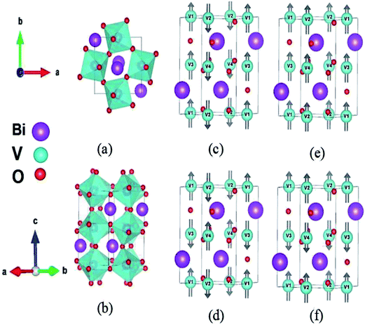 |
| | Fig. 1 Crystal and magnetic structures of Pbnm (also can be used as Pnma notation) phase of BiVO3 perovskites. Panel (a) is top view of Pbnm BiVO3. Panel (b) is bulk structure of Pbnm BiVO3. Panels (c), (e) and (f) are C-, A- and G-type antiferromagnetic ordered Pbnm BiVO3. Panel (d) is ferromagnetic ordered Pbnm BiVO3. Here, we use FM, A-AFM, C-AFM and G-AFM to mark ferromagnetic, A-, C- and G-type antiferromagnetic ordered Pbnm BiVO3, respectively. | |
3.2. Electronic properties of C-AFM structures of BiVO3
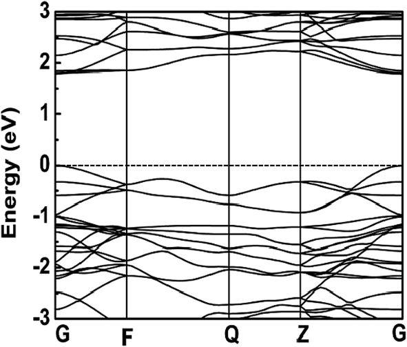
The result of calculated band structure is plotted in Fig. 2, where the dashed line represents the Fermi level. The energy's eigenvalue (eV) of the high symmetrical point K at the top of valence band Ev and the bottom of conduction band Ec in the first Brillouin-zone are shown in Table 2. In Table 2, the energy band of BiVO3 gets the maximum of 0 eV at point G in the valence band and the minimum of 1.79 eV at point G in the conduction band. Therefore, BiVO3 represents direct-gap with a gap width of 1.79 eV. In the valence band near the Fermi energy, the bands are due to the Bi-6s, O-2p, and a small contribution from V-3d orbitals. In the conduction band, the bands is mainly due to V-3d at lower part and the upper part are due to O-2p and V-3d orbitals.
 |
| | Fig. 2 Total DOS and partial DOS of BiVO3 and partial DOS for V, O, Bi ions in the C-AFM structure obtained by GGA (U = 3 eV). | |
Table 2 The energy's eigenvalue (eV) of the high symmetrical point K at the top of valence band Ev and the bottom of conduction band Ec in the first Brillouin-zone
| |
G |
F |
Q |
Z |
| Ev (eV) |
0 |
−0.3612 |
−0.5682 |
−0.3041 |
| Ec (eV) |
1.79 |
1.8505 |
2.1604 |
2.2519 |
Fig. 3 shows the total density of states (DOS) and partial DOS of C-AFM ordered BiVO3 structures in the energy range of −12 to 6 eV. The fermi energy levels are set to zero, majority and minority spins are showed above and below the axes. It should be noted that the lower bands in the range of −12 to −9 eV are formed by Bi-6s states with minor contribution from the O-2p states. The top of the valence band ranges from −7 to 0 eV shows that the valence band contains 2p electrons from O-ions, 6s electrons from Bi-ions. Furthermore, the top of the valence bands mainly due to strong hybridization effect of O-2p and Bi-6s and weak hybridization effect of V-3d and O-2p states, which suggest co-valent bonding contribution in BiVO3. For the C-AFM ordering, we calculated the local magnetic moments are 0.021μB, 1.812μB, 0.011μB, and 0.016μB for Bi, V, O(1), O(2), respectively. The local magnetic moments of Bi3+ is reduced from the formally 3μB, the reduction of local magnetic moments of Bi-ions and slight decrease of local magnetic moments of V-ions originate from the strong hybridization Bi–O and weak hybridization V–O.
 |
| | Fig. 3 Calculated band structure for BiVO3 in the C-AFM structure by GGA (U = 3 eV) along the high-symmetry axes of the Brillouin zone. The zero point of the energy is set at the top of valence bands and only the lowest few conduction bands are shown. | |
3.3. Born effective charges of BiVO3
The Born effective charges can be used to determine the nature of bonding. Thus, Born effective charges of C-AFM BiVO3 are calculated and shown in Table 3. The Born effective charge of an atom k is defined as:| |
 | (4) |
here, Pγ is the polarization induced by displacement τk,α of atom k. V is the unit cell volume of C-AFM BiVO3. The nominal charges of Bi, V and O are +3, +3 and −2 in the unit of |e|, respectively. From the Table 3, on the one hand, the xx, yy and zz components of Bi are around 63.6%, 64.3% and 65.6% larger than the static charge +3 of Bi, respectively. This occurs rather frequently in Bi-based oxides and thus indicates the obvious covalence effect of Bi–O bond. For example, in paraelectric R![[3 with combining macron]](https://www.rsc.org/images/entities/char_0033_0304.gif) c phase of BiFeO3, the value is about 41–69% larger than +3. Owing to the strong Bi-6p and O-2p hybridization, the Bi–O bond presents obvious covalent bonding behavior. On the other hand, the xx, yy and zz components of V are about 25.0%, 20.2% and 11.2% larger than the static charge +3 of V, respectively. This can be easily understood when noticing the fact that V3+ has d2 configuration. The non-d0 configuration25 is harmful to the covalence bonding behavior of V–O bond, thus the V-3d and O-2p hybridization is not that strong compared to Bi-6p and O-2p hybridization.
c phase of BiFeO3, the value is about 41–69% larger than +3. Owing to the strong Bi-6p and O-2p hybridization, the Bi–O bond presents obvious covalent bonding behavior. On the other hand, the xx, yy and zz components of V are about 25.0%, 20.2% and 11.2% larger than the static charge +3 of V, respectively. This can be easily understood when noticing the fact that V3+ has d2 configuration. The non-d0 configuration25 is harmful to the covalence bonding behavior of V–O bond, thus the V-3d and O-2p hybridization is not that strong compared to Bi-6p and O-2p hybridization.
Table 3 Calculated diagonal elements of Born effective charge tensor (in the unit of |e|) for antiferromagnetic BiVO3 in the C-AFM Pnma structures. Here, e is the charge of one electron
| Z* |
Position |
xx |
yy |
zz |
| Bi |
4c |
4.909 |
4.929 |
4.968 |
| V |
4b |
3.751 |
3.607 |
3.336 |
| O |
8d |
−3.161 |
−2.720 |
−2.707 |
| O |
4c |
−2.340 |
−3.099 |
−2.890 |
3.4 Optical properties
As all we known, we use the dielectric function ε(ω) = ε1(ω) + iε2(ω) to describe the optical response of the medium at all photon energies. The imaginary part ε2(ω) of the dielectric constant is directly related to the electronic band structure of a material and describes the absorptive behavior. In this paper, the imaginary part ε2(ω) is given by:26,27| |
 | (5) |
here, M is the dipole matrix, i and j are the initial and final states respectively, fi is the Fermi distribution function for the i-th state, and Ei is the energy of electron in the i-th state with the crystal wave vector k. The real part ε1(ω) of the dielectric function can be extracted from the imaginary part using the Kramers–Kronig relation in the form:28,29| |
 | (6) |
here, P implies the principal value of the integral. The absorption, refractive index, loss function and other optical properties can be obtained from the dielectric function.| |
 | (7) |
| |
 | (8) |
The real (dispersive) and imaginary (absorptive) parts of the dielectric function, reflectivity and energy loss function are shown in Fig. 4(a)–(c). The imaginary ε2(ω) and real ε1(ω) parts of the dielectric function are shown in Fig. 4(a), as functions of the photon energy in the range 0–5 eV. In the imaginary ε2(ω), there are mainly 4 peaks observed at 2.12 eV, 2.93 eV, 4.32 eV and 4.74 eV. The peaks originate from the electronic transitions from V-3d state in the valence band to the V-3d state in the conduction band. The real ε1(ω) part of the dielectric function gives us information about the electronic polarizability of the material. It keeps above 0 in the energy region from 0 eV to 4.55 eV. There are mainly 3 peaks observed at 1.85 eV, 2.82 eV and 3.58 eV. After a considerable decline started from 3.58 eV, it reaches a minimum with a negative value. At negative values of real dielectric function ε1(ω), this material shows the metallic behavior in these energy parts. The energy loss function obtained from the complex dielectric represents the energy loss by electrons passing through a homogeneous dielectric material, shown in Fig. 4(c). Transitions between the occupied and unoccupied states, which are predominantly induced by the electric field of the photon, are known as Plasmon's. The energy loss curve generally has a sharp peak near the plasma frequency, which is 2.2 eV, where the longitudinal charge fluctuation occurs. The peak of the energy loss function is associated with the abrupt reduction in the reflectivity curve. For example, the sharp peak in the loss function is situated at approximately 4.7 eV, corresponding to a drastic reduction in the reflective curve.
 |
| | Fig. 4 GGA+U results of (a) the dielectric function ε(ω), (b) optical reflective spectrum R(ω), (c) energy loss spectrum and refractive index (d) the absorption coefficient of C-AFM BiVO3. | |
To evaluate the potentiality for optoelectronic applications we have obtained the optical absorption coefficients, shown in Fig. 4(d). It is obvious that, when the photon energy is more than 1.79 eV, the absorption coefficient start increase, corresponding to the direct band gap 1.79 eV, which originates from the hybridization of O-2p and V-3d, which will somewhat relax the parity selection rule and result in a non-zero transition probability. The absorption coefficient will get maximum value 7.0 × 105 cm−1 when the photon energy is 5 eV, which belongs to the ultra-violet region. It is well known that, visible light region is in the range of 1.64 to 3.19 eV or 740–370 nm. Additionally, analysis of the absorption and the reflectivity of BiVO3 also show that the BiVO3 bulk has low reflection efficiency in the visible light range. These properties make the BiVO3 as a promising photocatalyst with favorable photocatalytic activity in the visible region.
4. Conclusions
In summary, we have carried out first-principles calculations in order to address the possible crystal and magnetic structures as well as the electronic structures of perovskite BiVO3 oxides. The Pnma with C-type antiferromagnetic order is suggested as the possible ground of bulk BiVO3 oxides. The strong Bi-6p and O-2p hybridization lead to that the Born effective charge of Bi is almost 65% larger than the static charge +3. Furthermore, from the knowledge of the real and imaginary part of the dielectric function ε(ω), refractive and n(ω), reflectivity spectrum R(ω) and the absorption coefficient α(ω), BiVO3 has high absorption power and low reflectivity efficiency in the visible and ultraviolet energy range, so it can be in the optoelectronic devices such as UV detectors, and can also be used in anti-reflection coatings.
Acknowledgements
The authors express their thanks to the changsha Supercomputer Center for computation. This work has been supported by the National Natural Science Foundation of China through Grant No. 51172067, the Hunan Provincial Natural Science Fund for Distinguished Young Scholars through Grant No. 13JJ1013, the Specialized Research Fund for the Doctoral Program of Higher Education through Grant No. 20130161110036, and the New Century Excellent Talents in University through Grant NCET-12-0171. D.
References
- R. Maeda, Photocatalytic water splitting using semiconductor particles: history and resent developments, J. Photochem. Photobiol., C, 2011, 12, 237–268 CrossRef.
- J. A. McLeod, Z. V. Pchelkina, L. D. Finkelstein, E. Z. Kurmaev, R. G. Wilks, A. Moewes, I. V. Solovyev, A. A. Belik and E. Takayama-Muromachi, Electronic structure of BiMO3 multiferroics and related oxides, Phys. Rev. B: Condens. Matter Mater. Phys., 2010, 81, 144103 CrossRef.
- S. Murugesan, M. N. Huda, Y. F. Yan, M. M. Al-Jassim and V. Subramanian, Band-Engineered Bismuth Titanate Pyrochlores for Visible Light Photocatalysis, J. Phys. Chem. C, 2010, 114, 10598–10605 CAS.
- S. Li, Y. H. Lin, B. P. Zhang, Y. Wang and C. W. Nan, Controlled Fabrication of BiFeO3 Uniform Microcrystals and Their Magnetic and Photocatalytic Behaviors, J. Phys. Chem. C, 2010, 114, 2903–2908 CAS.
- R. Q. Guo, L. Fang, W. Dong, F. G. Zheng and M. R. Shen, Enhanced Photocatalytic Activity and Ferromagnetism in Gd Doped BiFeO3 Nanoparticles, J. Phys. Chem. C, 2010, 114, 21390–21396 CAS.
- N. A. Hill, P. Battig and C. Daul, First principles search for multiferroism in BiCrO3, J. Phys. Chem. B, 2002, 106, 3383–3388 CrossRef CAS.
- A. A. Belik, S. Iikubo, K. Kodama, N. Igawa, S. Shamoto, S. Niitaka, M. Azuma, Y. Shimakawa, M. Takano, F. Izumi and E. Takayama-Muromachi, Neutron powder diffraction study on the crystal and magnetic structures of BiCoO3, Chem. Mater., 2006, 18, 798–803 CrossRef CAS.
- M. Q. Cai, G. W. Yang, X. Tan, Y. L. Cao, L. L. Wang, W. Y. Hu and Y. G. Wang, First-principles study of pressure-induced metal-insulator transition in BiNiO3, Appl. Phys. Lett., 2007, 91, 101901 CrossRef.
- I. V. Solovyev and Z. V. Pchelkina, Magnetic-field control of the electric polarization in BiMnO3 (vol 82, 094425, 2010), Phys. Rev. B: Condens. Matter Mater. Phys., 2014, 90, 094425 Search PubMed.
- M. Azuma, S. Niitaka, N. Hayashi, K. Oka, M. Takano, H. Funakubo and Y. Shimakawa, Rhombohedral-tetragonal phase boundary with high curie temperature in (1 − x)BiCoO3–xBiFeO(3) solid solution, Jpn. J. Appl. Phys., 2008, 47, 7579–7581 CrossRef CAS.
- M. Q. Cai, J. C. Liu, G. W. Yang, Y. L. Cao, X. Tan, X. Y. Chen, Y. G. Wang, L. L. Wang and W. Y. Hu, First-principles study of structural, electronic, and multiferroic properties in BiCoO3, J. Chem. Phys., 2007, 126, 154708 CrossRef PubMed.
- M. Azuma, W. T. Chen, H. Seki, M. Czapski, S. Olga, K. Oka, M. Mizumaki, T. Watanuki, N. Ishimatsu, N. Kawamura, S. Ishiwata, M. G. Tucker, Y. Shimakawa and J. P. Attfield, Colossal negative thermal expansion in BiNiO3 induced by intermetallic charge transfer, Nat. Commun., 2011, 2, 347 CrossRef PubMed.
- M. Q. Cai, X. Tan, G. W. Yang, L. Q. Wen, L. L. Wang, W. Y. Hu and Y. G. Wang, Giant Magneto-Optical Kerr Effects in Ferromagnetic Perovskite BiNiO(3) with Half-Metallic State, J. Phys. Chem. C, 2008, 112, 16638–16642 CAS.
- M. P. S. a. F. S. Razavi, Structural and Physical Properties of BiVO3, Conference Proceedings, 2013, 1590, 90–94 Search PubMed.
- M. Dragomir and M. Valant, Synthesis peculiarities of BiVO3 perovskite, Ceram. Int., 2013, 39, 5963–5966 CrossRef CAS.
- D. J. Payne, M. D. M. Robinson, R. G. Egdell, A. Walsh, J. McNulty, K. E. Smith and L. F. J. Piper, The nature of electron lone pairs in BiVO4, Appl. Phys. Lett., 2011, 98, 212110 CrossRef.
- R. H. Mitchell, Perovskites, Modern and Ancient, almaz Press, 2002 Search PubMed.
- M. W. Lufaso and P. M. Woodward, Prediction of the crystal structures of perovskites using the software program SPuDS, Acta Crystallogr., Sect. B: Struct. Sci., 2001, 57, 725–738 CrossRef CAS PubMed.
- B. Liu, L. J. Wu, Y. Q. Zhao, L. Z. Wang and M. Q. Cai, Tuning the Schottky barrier height of the Pd–MoS2 contact by different strains, Phys. Chem. Chem. Phys., 2015, 17, 27088–27093 RSC.
- Y.-Q. Zhao, L.-J. Wu, B. Liu, L.-Z. Wang, P.-B. He and M.-Q. Cai, Tuning superior solar cell performance of carrier mobility and absorption in perovskite CH3 NH3 GeCl3: a density functional calculations, J. Power Sources, 2016, 313, 96–103 CrossRef CAS.
- B. Liu, L. J. Wu, Y. Q. Zhao, L. Z. Wang and M. Q. Cai, Tuning the Schottky contacts in the phosphorene and graphene heterostructure by applying strain, Phys. Chem. Chem. Phys., 2016, 18, 19918–19925 RSC.
- V. Stevanovic, S. Lany, X. W. Zhang and A. Zunger, Correcting density functional theory for accurate predictions of compound enthalpies of formation: fitted elemental-phase reference energies, Phys. Rev. B: Condens. Matter Mater. Phys., 2012, 85, 115104 CrossRef.
- H. J. Koo and M. H. Whangbo, Determination of the Spin-Lattice Relevant for the Quaternary Magnetic Oxide Bi4Cu3V2O14 on the Basis of Tight-Binding and Density Functional Calculations, Inorg. Chem., 2008, 47, 4779–4784 CrossRef CAS PubMed.
- E. Garcia-Ramirez, M. Mondragon-Chaparro and O. Zelaya-Angel, Band gap coupling in photocatalytic activity in ZnO–TiO2 thin films, Appl. Phys. A: Mater. Sci. Process., 2012, 108, 291–297 CrossRef CAS.
- J. M. Rondinelli, A. S. Eidelson and N. A. Spaldin, Non-d(0) Mn-driven ferroelectricity in antiferromagnetic BaMnO3, Phys. Rev. B: Condens. Matter Mater. Phys., 2009, 79, 205119 CrossRef.
- S. Gong, Y. H. Wang, X. Y. Zhao, M. Zhang, N. Zhao and Y. F. Duan, Structural, Electronic and Optical Properties of BiAlxGa1–xO3 (x = 0, 0.25, 0.5 and 0.75), Chin. Phys. Lett., 2011, 28, 8 CrossRef.
- S. K. Cushing, J. T. Li, F. K. Meng, T. R. Senty, S. Suri, M. J. Zhi, M. Li, A. D. Bristow and N. Q. Wu, Photocatalytic Activity Enhanced by Plasmonic Resonant Energy Transfer from Metal to Semiconductor, J. Am. Chem. Soc., 2012, 134, 15033–15041 CrossRef CAS PubMed.
- H. Amorin, R. Jimenez, E. Vila, M. Dolle, A. Castro and M. Alguero, Electrical properties of ferroelectric BiMnO3–PbTiO3 under tailored synthesis and ceramic processing, Phase Transitions, 2013, 86, 681–694 CrossRef CAS.
- L. Y. Gan, Q. Y. Zhang, Y. C. Cheng and U. Schwingenschlogl, Two-dimensional ferromagnet/semiconductor transition metal dichalcogenide contacts: p-type Schottky barrier and spin-injection control, Phys. Rev. B: Condens. Matter Mater. Phys., 2013, 88, 235310 CrossRef.
Footnote |
| † Electronic supplementary information (ESI) available. See DOI: 10.1039/c6ra17053f |
|
| This journal is © The Royal Society of Chemistry 2016 |
Click here to see how this site uses Cookies. View our privacy policy here. 
 , wherein rA, rO, rB are the ionic radii of A, B, and O ions, respectively.17 For t = 1, perovskite oxides crystallize in a cubic symmetry, for 1 > t > 0.95, it adopts to a tetragonal symmetry and for 0.95 > t > 0.8, either the orthorhombic or the monoclinic symmetry.17 Taking rV3+ = 78 pm, rO2− = 128 pm, and rBi3+ = 117 pm in octahedral coordination, the calculated value of t is about 0.84 for BVO. So, this article we will adopt either monoclinic or pnma orthorhombic crystal symmetry akin to the LaVO3.14 The structure is predicted by the SPUDS18 software has been used as a starting point. Geometry optimization has been performed within the monoclinic (C2/c) and the orthorhombic (pnma) structures of BVO. The optimized lattice and atomic positions of BVO with two structures are shown in Table 1. As we will see, the Table 1 shows that the total energy of the Pnma phase is lower than the C2/c, and thus we take the Pnma crystal symmetry for the further calculations. Then, four magnetic structures are considered in Pnma phase of BiVO3. The calculations are performed by VASP code.19 The generalized gradient approximation (GGA, in the framework of PBE20,21) are used as exchange and correlation functional. Because the coulomb interaction of 3d electrons of V3+ ions is very strong, we employ the GGA+U method in the present calculations and use a Hubbard U parameter of 3.0 eV.22 We choose plane-wave energy cutoff is 500 eV and the (6 × 4 × 6) k-point mesh in calculations. The structural optimization is carried out by the conjugate-gradient algorithm until the Hellmann–Feynman force is less than 0.005 eV Å−1 assuming magnetic ordering. The valence configurations for Bi, V and O are 5d106s26p3, 3p3d34s2, 2s22p4, respectively.