
 Open Access Article
 This Open Access Article is licensed under a
 Creative Commons Attribution 3.0 Unported Licence
Charge transfer plasmon resonances across silver–molecule–silver junctions: estimating the terahertz conductance of molecules at near-infrared frequencies
Lin
Wu
*a,
Shu Fen
Tan
b,
Michel
Bosman
cd,
Joel K. W.
Yang
ce,
Christian A.
Nijhuis
bf and
Ping
Bai
*a
aInstitute of High Performance Computing, A*STAR (Agency for Science, Technology and Research), 1 Fusionopolis Way, 16-16 Connexis North, Singapore 138632. E-mail: wul@ihpc.a-star.edu.sg; baiping@ihpc.a-star.edu.sg
bDepartment of Chemistry, National University of Singapore, 3 Science Drive 3, Singapore 117543
cInstitute of Materials Research and Engineering, A*STAR, 2 Fusionopolis Way, Singapore 138634
dDepartment of Materials Science and Engineering, National University of Singapore, 9 Engineering Drive 1, Singapore 117575
eSingapore University of Technology and Design, 8 Somapah Road, Singapore 487372
fCenter for Advanced 2D Materials, National University of Singapore, 2 Science Drive 3, Singapore 117542
First published on 19th July 2016
Abstract
Quantum plasmon resonances have been recently observed across molecular tunnel junctions made of two plasmonic resonators bridged by a self-assembled monolayer (SAM). The energy of this quantum plasmon mode, i.e., the tunneling charge transfer plasmon (tCTP), depends on the properties of the molecules bridging the gaps. The present work extends these studies theoretically using a generalized space-charge corrected electromagnetic model to a wider range of SAM structures (with various molecular lengths and conductances) sandwiched between silver nanocubes, which could support different types of CTP resonances in addition to tCTP. The space-charge corrected electromagnetic model treats the charge injection and charge transport separately, and assumes a Drude expression (with damping frequency on the order of driving frequency) to model the space-charge limited transport problem. Our theoretical modelling of these organic–inorganic hybrid structures establishes a one-to-one relationship between the conductivity of the SAM and the resonant energy of the CTP modes. Considering that the SAM consists of a finite number of molecules bridging the two nanocubes in a parallel arrangement, we introduce a method to estimate the molecular conductance at the CTP resonant frequency. Experimental results from two types of SAMs were examined as a proof-of-concept: the THz conductance is estimated to be 0.2G0 per EDT (1,2-ethanedithiolate) molecule at 140 THz and 0.4G0 for a BDT (1,4-benzenedithiolate) molecule at 245 THz. This approach paves the way of using plasmonic oscillations for measuring the THz conductance of single molecules at near-infrared frequencies.
Introduction
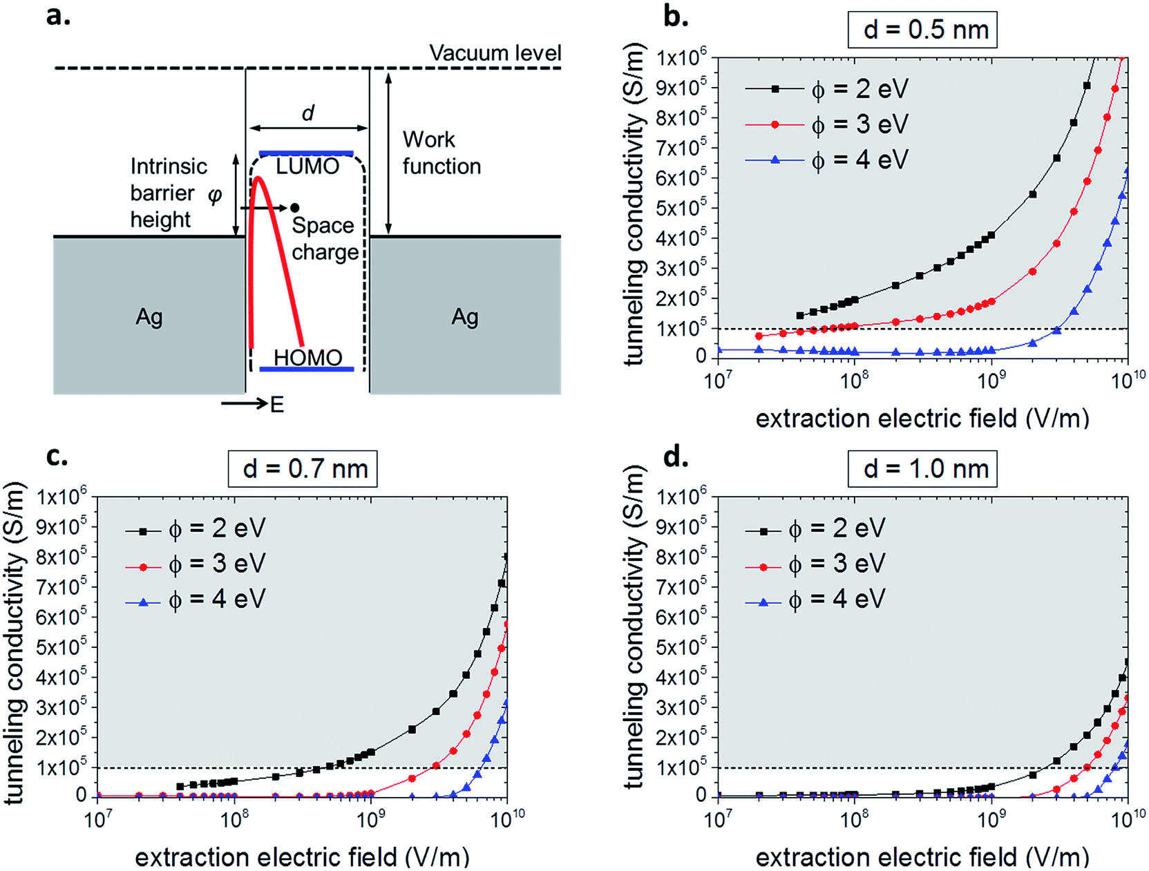
In the past decade, there has been significant progress in understanding the optical properties of plasmonic nanostructures.1–5 A unique feature of plasmonic nanostructures is the sensitive dependence of their plasmon resonance energies on nanostructure geometry and dielectric environment. This property lays the foundation for one of its most promising applications – plasmonic sensing.6–8 In particular, there is one type of plasmon resonance, the charge transfer plasmon (CTP), which has drawn a lot of attention in recent years because it becomes important at atomic length scales.9–25 This charge transfer plasmon usually occurs across an optically-conductive junction between two nanoparticles, and its plasmon resonance energy is particularly sensitive to the shape and conductivity of the junction. This property of CTPs opens the door to many new applications such as single molecule sensing,21 optical nanoswitches,14 probes for molecular conductance at optical frequencies15 and so on.Depending on the conduction mechanism of the junctions, different types of CTP resonances can be classified. The first type comprises the metallic or semiconductor junction, where the conduction mechanism is free carrier (e.g., free electron) transport. Dimers that are linked by a thin metal bridge are able to generate a CTP with a resonance typically in the near-infrared region of the spectrum.2,12,21 By filling the dimer gap with semiconducting materials (e.g., amorphous silicon), the frequency of the CTP can be controlled as progressive photoconductive gap-loadings are achieved (theoretically) by varying the free-carrier density of the semiconductor.14 The second type refers to dielectric junctions, including air gaps, vacuum gaps, and inorganic/organic dielectric films. In contrast to a bridge made of a metal or semiconductor, no free carrier is available in the dielectric films. The mechanism of charge transport between the two plasmonic resonators is quantum mechanical tunneling. For junctions with high tunneling rates (i.e., for small gaps with low tunneling barrier heights), tunneling charge transfer plasmon (tCTP) can be observed.13,16–19
In this work, we use a platform that could support various types of CTPs, which consists of a self-assembled monolayer (SAM) connecting two metallic nanoparticles, forming a SAM-bridged plasmonic dimer. We use this platform to probe the molecular conductance at terahertz frequencies. Within a SAM-bridged plasmonic dimer, the molecular junction is typically characterized by molecular frontier orbitals, i.e., the highest occupied molecular orbital (HOMO) and the lowest unoccupied molecular orbital (LUMO). The properties of molecular junctions depend on many factors, e.g., molecule-electrode interactions strength, chemical structure of the molecule, nature of the molecule-electrode contacts, etc., which make it possible to control the electrical and optical properties of molecular junctions by altering the chemical structure of the molecule. For example, conjugated molecules are considered to be more conductive than aliphatic molecules due to their small HOMO–LUMO gaps; this property has been used to tune the frequency of tCTP in molecular tunneling junctions.20 In other work, incremental replacement of the nonconductive molecules with a chemically equivalent conductive version differing by only one atom has produced a strong 50 nm blue-shift of the coupled plasmon.25 Standard DC or low-frequency electrical transport measurements in molecular electronics26,27 cannot be performed at near-infrared frequencies (i.e., 200–400 THz or 0.75–1.5 μm). Characterization of charge transfer plasmons through molecular junctions could fill this unexplored regime, probing molecular conductance at frequencies of hundreds of terahertz.
It is challenging to model the optical response of the SAM-bridged plasmonic dimers for three reasons: (I) multiscale: the length-scales of the plasmonic metal electrodes and molecular monolayers are very different, e.g., the electrode is a cube with side-length of a few tens of nanometres consisting of heavy Ag atoms, and the SAM consists of many molecules made up of light C and H atoms with molecular length on the order of one nanometer;20 (II) interface: the electron transport/transfer processes in metals and molecules are distinct, which makes the modelling of the continuous charge transfer through the metal/SAM interface difficult, even at DC frequency; and (III) multiphysics: the problem involves at least two non-negligible physical processes, which include plasmonic oscillation and charge transport. To solve the problem, three modelling methods are available at present. First of all, full quantum-mechanical first-principles calculations26,27 should be the most accurate method to capture the multiple physics in this problem, but it becomes impractical when the large number of electrons in the plasmonic electrodes needs to be taken into account.17 Second, classical electromagnetic models are the most popular models to describe the optical response of plasmonic systems due to their simplicity, but they only deal with electromagnetics and not with charge transport. In certain circumstances where additional physics (e.g., photoexcitation14 and quantum tunneling17,19,22–24) is involved, part of the nanostructure cannot be modeled by its conventional local linear dielectric function and corrected electromagnetic models are more appropriate. The corrected electromagnetic models divide the multiphysics problem into two parts: (I) a fictitious junction material (whose local permittivity is characterized using a Drude model) is introduced, representing the additional physical phenomenon other than electromagnetics; and (II) with the inclusion of the fictitious junction material, the optical/plasmonic properties are calculated within the classical electromagnetic framework. Compared to the full quantum-mechanical calculations and classical electromagnetic models, the corrected electromagnetic models are simple, fast and capable of modelling multiphysics problems. The most representative example, the quantum-corrected model (QCM)17 that is used to model quantum tunneling junctions, has recently attracted a lot of attention and been extended to model different junction morphologies,22 to improve its accuracy for practical situations,23 and also to different numerical implementations.24 However, the essence of QCM does not change – the introduction of the fictitious junction.
For the SAM-bridged plasmonic dimers, we will employ the same corrected electromagnetic models by introducing a fictitious junction material. However, different from those available in the literature, our model further breaks down the problem by separately modelling the following two processes: the ‘charge injection at the metal/SAM interface’ and ‘charge transport in the fictitious junction material’. We will use a space-charge model (applicable to both classical28 and quantum29 regimes) to correlate the charge injection and charge transport parts. In doing so, a frequency-dependent ac conductivity of the fictitious junction material (i.e., the space-charge region) is used. This frequency-dependent ac conductivity is critical to show the dependence of the CTP resonance energy on the conductivity of the SAM.
By using the frequency-dependent ac conductivity for the fictitious junction, we have successfully explained our experimental findings of tCTP in our first two sets of molecular tunneling junctions.20 The present work will further develop the technique to a more comprehensive and generalized model, namely, the space-charge corrected electromagnetic model. Making use of this generalized model, we will conduct a thorough theoretical investigation of the charge transfer plasmons across the molecular junctions in silver nanoparticle–SAM–silver nanoparticle dimer systems, for a wide range of molecules with different lengths and optical conductivities. Our theoretical modelling of these dimer systems establishes a one-to-one relationship between the conductance of the SAM layer and the resonant energy of the CTP mode. Based on the finding, we will demonstrate in this work the application of using plasmonic oscillations for measuring the terahertz conductance of single molecules at near-infrared frequencies.
Results and discussion
Space-charge corrected electromagnetic model
Fig. 1a shows the hybrid dimer system that we use to study single molecule terahertz conductance using plasmon characterization. In this dimer system, cuboidal Ag nanoparticles are functionalized with SAMs, forming metal–SAM–metal junctions through self-assembly. Through optimization of the self-assembly process, these dimeric structures with a single layer of well-aligned SAMs are useful systems to study the molecular conductance at near-infrared plasmon frequencies.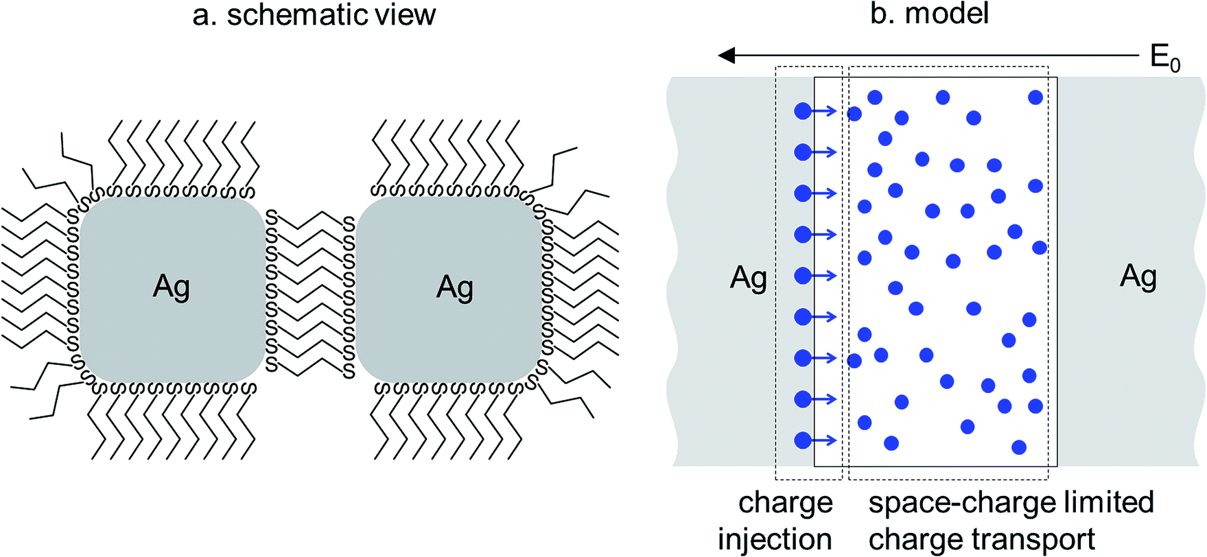 | ||
Fig. 1 (a) Schematic diagram of the hybrid dimer system: an Ag–SAM–Ag junction. Not drawn to scale, e.g., there are ∼16![[thin space (1/6-em)]](https://www.rsc.org/images/entities/char_2009.gif) 000 saturated, aliphatic 1,2-ethanedithiolate (EDT) molecules in a 37 × 37 nm2 junction.20 (b) The space-charge corrected electromagnetic model to describe the charge transfer plasmon oscillations for the Ag–SAM–Ag junction: negative driving field (during half cycles) induces charge transfer from left to right. Two physical processes are proposed in the model: charge injection at the Ag/SAM interface and charge transport inside the fictitious junction forming a space-charge region. 000 saturated, aliphatic 1,2-ethanedithiolate (EDT) molecules in a 37 × 37 nm2 junction.20 (b) The space-charge corrected electromagnetic model to describe the charge transfer plasmon oscillations for the Ag–SAM–Ag junction: negative driving field (during half cycles) induces charge transfer from left to right. Two physical processes are proposed in the model: charge injection at the Ag/SAM interface and charge transport inside the fictitious junction forming a space-charge region. | ||
More specifically, we describe our Ag–SAM–Ag systems using a space-charge corrected electromagnetic model as shown in Fig. 1b. Our model separates the ‘charge injection’ and ‘charge transport’ processes. The rationale behind this separation is that, the commonly-used Drude model (to describe the fictitious junction material) within the classical/corrected electromagnetic framework assumes that the motion of electrons is damped via collisions, but the charge injection at the interface (e.g., through quantum tunneling or field emission) is often a collision-free or ballistic transport process. It remains questionable to model a ballistic transport process using a Drude model. By breaking down the problem, we can consider the electron collisions in the ‘charge transport’ region, but not in the ‘charge injection’ process.
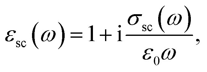
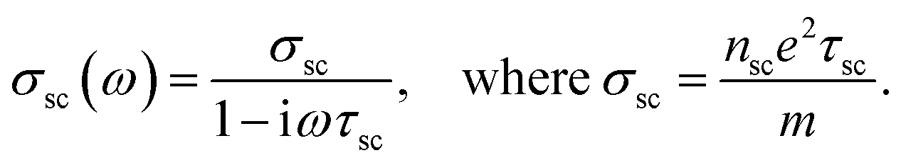
As shown in Fig. 1b, the ‘charge injection’ process defines the number density of free electrons that are able to escape out of the metal into the SAM layer: nsc, where ‘sc’ stands for space charge. Space charge is a concept in which excess electric charge is treated as a continuum of charge distributed over a region of space (usually dielectrics) rather than distinct point-like charges. This model typically applies when charge carriers have been emitted from a solid. The well-known classical Child's Law28 that defines the space-charge limited current (SCLC) in a plane-parallel vacuum diode has been theoretically extended to the quantum tunneling regime for diodes with nanometer-scale gaps.29 Here, we apply the same concept to model the charge injection from the plasmonic metal electrode into the SAM layer, where a space-charge region forms in the fictitious junction material. It is these nsc free electrons that transport in the space charge region with a damping frequency γsc. Their optical properties are therefore described using the Drude model:30
 | (1) |
 | (2) |
By rearranging the terms in eqn (1) and (2) into a form that can be directly compared to the pioneer quantum-corrected model by Esteban et al.17 that was used to describe tunneling junctions, we have:
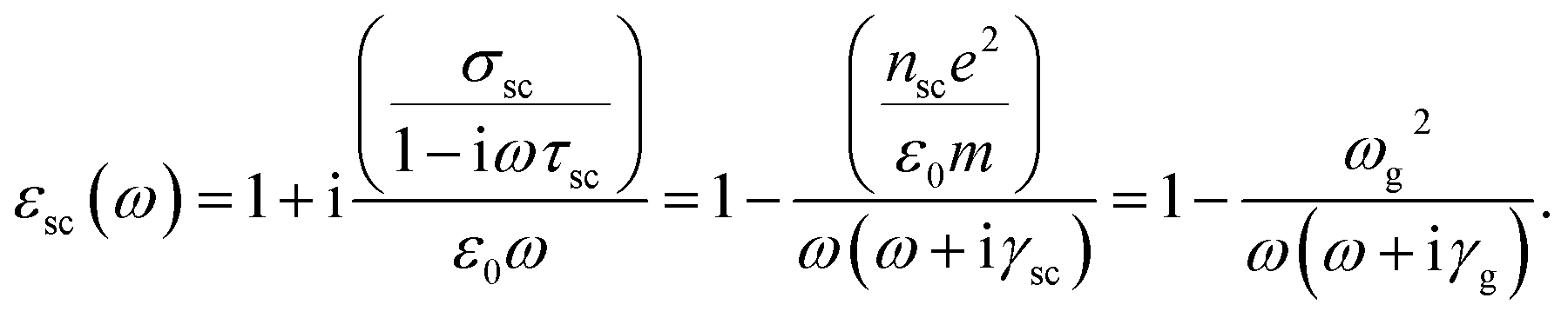 | (3) |
It is clear that (I) our damping frequency γsc in the space charge region (i.e., the characteristic collision frequency) is analogous to their tunneling damping parameter γg (but with different damping mechanisms); (II) they use plasma frequency 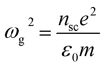 to represent the number density of free charges nsc in the space charge region, while we use conductivity
 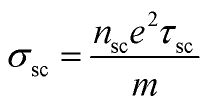 since we are interested in conductance measurements. Up to this point, the two models are essentially the same in mathematical form, although physically different. Our model highlights the individual (but correlated) modelling of the collision-free ‘charge injection’ part at the interface (which determines nsc) and the ‘space charge region’ part within the fictitious junction (described by the electron-collisions based Drude model eqn (3)). However, their model specifically assumes that tunneling γg ≫ ω and only dc conductivity of the fictitious junction is considered, where the frequency dispersion of the conductivity is neglected.17 In fact, a recent theoretical study31 has suggested that the tunneling damping γg can be significantly reduced (up to 4 orders) by increasing the tunneling rate to reach the space-charge-limited regime. Here we aim to develop a more generalized model, so we remove this assumption and use the full expression of εsc(ω). The two parameters nsc and γsc (or τsc = 1/γsc) are used to take care of various charge injection and transport mechanisms.
Physically, within the space charge region, the relaxation time τsc is a function of the number density of free carriers nsc: more densely distributed free carriers tend to collide more frequently, giving a shorter τsc. However, the exact relation between the two is unknown (to the best of our knowledge). Previously, we predicted that the number density of the injected free electrons needs to be close to that of the metal (on the order of 1028 m−3) in order to trigger the CTP mode,19 while the relaxation time of the free electron gas in metals is typically on the order of 10 fs at room temperature.30 Therefore, τsc = 10 fs is assumed throughout this study. Numerically, the resonant energy of 0.3–3 eV corresponds to a driving frequency ω of 72.5–725 THz, whereas the damping frequency of the free electron in the space charge region γsc is on the order of 100 THz. These comparable frequency scales also support the usage of frequency-dependent ac conductivity in the space charge region.
However, it should be noted here that the proposed space-charge corrected electromagnetic model does not capture the detailed atomic-scale interactions32 between the injected electrons and the molecule atoms in the ‘charge transport’ part. The critical properties of a SAM layer (e.g., HOMO–LUMO gap, alignment of HOMO–LUMO with respect to the Fermi-level of the metal, molecular length, etc.) are all taken into account by the ‘charge injection’ modelling part (to be discussed in latter section of Charge injection mechanisms).
Before treating any specific charge injection mechanisms, we first classically simulate the plasmon resonances of the Ag–SAM–Ag systems for different types of SAMs by using two variables as input parameters: (I) the molecular length d of SAMs and (II) the conductivity σsc of the SAM charge transport layer, which is directly relevant to the number density of free electrons that are able to be injected from one electrode into the space charge region. Therefore, a map of plasmon resonant energy ħωCTPversus the molecular length and conductivity of the SAMs can be compiled which can be used as a benchmark for subsequent investigations. Experimental measurements of the plasmon resonance of a particular type of the SAM then allow us to estimate the conductivity of that SAM layer. By knowing the number of molecules in the SAM layer, we can subsequently estimate the conductance of each single SAM molecule.
Simulated plasmon resonance of Ag–SAM–Ag systems
The plasmon resonances of Ag–SAM–Ag systems are simulated using finite-element-method (FEM) optical simulations. The spectra of absorption, scattering and their sum (i.e., extinction) for the Ag–SAM–Ag system are calculated. Simulations are performed using plane-wave excitation by assuming that the incident light is polarized along the longitudinal axis. Here the two identical Ag cuboids are assumed to have a square cross-section with side-length w and length l. The dielectric function of Ag is taken from Palik's handbook.33 Between the two Ag cuboids, the SAM layer is assumed to have a square cross section with area A = w × w nm2 and the length of the SAM layer d is determined by the molecular length. As the SAM layer now functions as the electron transport medium, it should not be described by its conventional refractive index. Instead, we assume the SAM layer as a fictitious junction material, and employ the corrected electromagnetic model using eqn (1) and (2) to simulate the system.Fig. 2 shows simulated plasmon resonance spectra of one representative Ag–SAM–Ag system for d = 0.5 nm. Various assumed conductivities σsc (S m−1) are simulated with values varying from perfectly insulating vacuum (σsc = 0) to highly conductive Ag (σsc is approximately on the order of 107 S m−1). It is interesting to note that the two extreme cases of a vacuum gap (top spectrum) and Ag gap (bottom spectrum) in Fig. 2a show a very similar spectral peak close to 2.5 eV. However, the modes are distinct, as shown in Fig. 2b (top and bottom). The vacuum gap case shows a bonding dipole plasmon (BDP) mode (“−” “+” “−” “+”) whereas the Ag gap case presents a charge transfer plasmon (CTP) mode (“−” “+”). When the conductivity of the SAM layer is gradually reduced from Ag to vacuum (from bottom to top in Fig. 2a), the spectra show smooth transitions: (I) the CTP modes continue to shift to lower energy with reduced magnitude (to finally disappear for σsc < 105 S m−1), (II) the BDP modes only appear for less conductive gap media with σsc < 1.5 × 10⁶ S m−1 and their resonance energies are hardly sensitive to changes in the gap conductivity, in contrast to the CTP modes.
 | ||
| Fig. 2 (a) Simulated extinction spectra with varying gap conductivities (ranging from insulating vacuum to highly conductive Ag) for an Ag–SAM–Ag system with the following dimensions: cross-sectional area = 37 × 37 nm2, length of each Ag cuboid = 35 nm, and length of the SAM in the gap d = 0.5 nm. Two plasmon modes are identified: charge transfer plasmons (CTPs) as indicated by the circular symbols and bonding dipolar plasmons (BDPs) as indicated by the triangular symbols. (b) Mode images (top view) for three selected SAM's conductivities are shown: (i) BDP with low conductivity σsc = vacuum; (ii) BDP and (iii) CTP with moderate conductivity σsc = 5 × 10⁵ S m−1; and (iv) CTP with high conductivity σsc = Ag. (c) Magnitudes of total electric field enhancements at the Ag/SAM interface (cross-sectional view) for various gap conductivities at their respective CTP resonant frequencies. | ||
According to the observations above, we can divide all the Ag–SAM–Ag junctions with different gap conductivities into three regimes as shown in Fig. 2a: low conductivity regime (<105 S m−1), moderate conductivity regime (105 to 1.5 × 10⁶ S m−1), and high conductivity regime (>1.5 × 10⁶ S m−1). In low conductivity regime, only BDP is supported; whereas in high conductivity regime, only CTP is supported. However, for moderate conductivity regime, both CTP and BDP are supported. One example of 5 × 10⁵ S m−1 is demonstrated in Fig. 2b where the mode images of BDP and CTP are shown in central panels (ii) and (iii) respectively. The co-existence of the two modes suggests that these Ag–SAM–Ag junctions with moderate conductivities behave like leaky capacitors. This can be also proved by the calculated gap field enhancements for CTP resonance (shown in Fig. 2c), where the gap fields are enhanced by a factor up to 200 for moderate conductivities (up to 1.5 × 10⁶ S m−1).
The field enhancement is found to increase with the gap conductivity till a critical value of σsc = 106 S m−1; then it drops as the conductivity further increases. To explain this, capacitance model could be used (the details of the model can be found later in “Measured data” section). Briefly, there are two competing mechanisms to influence the junction fields. First, the energy stored in the capacitor can be taken as the energy of a single plasmon. As the conductivity increases, the energy of the single CTP plasmon increases or shifts to right as indicated in Fig. 2a, therefore the energy stored in the capacitor (and hence the average electric field in the junction) will be increased accordingly. Second, if the stored energy in the capacitor keeps the same, a leakier capacitor or a more conductive junction leads to a lowered junction field. Our calculation in Fig. 2c suggests that the first mechanism dominates for junction conductivity smaller than 106 S m−1; while the second mechanism dominates for conductivity greater than 106 S m−1. In fact, for further increased junction conductivities (>2 × 10⁶ S m−1) that fall into the high conductivity regime, the junction fields drop quickly to zero at the CTP resonance as shown in Fig. 2c. We cannot use the capacitance model anymore, because these Ag–SAM–Ag systems behave like conductors.
This sensitivity of the CTP resonance energy ħωCTP to σsc establishes the basis of measuring the THz conductivity of SAM layers using the CTP plasmon resonance. Variation of conductivities from 105 to 5 × 10⁶ S m−1 would induce a change of CTP energy from 0.6 to 2.5 eV in this case, indicating a rather broad tunability. The conductivity-dependence of the CTP energy can be understood by the following simple physical picture. First, we understand that a minimum number of electrons need to participate in a charge transfer plasmon oscillation for a CTP resonant peak to appear in the spectrum. As the gap region is less capable of transferring electrons, it takes a longer time to transfer this minimum number of electrons across the gap. Macroscopically, the CTP resonance slows down and shifts to lower energy (or lower frequency).
While the current study focuses on the conductivity-dependence of the CTP energy (by fixing the geometry of the junction), most of the studies in the literature (e.g., CTP over metallic bridges2,21) in fact concentrated on the dependence of the CTP energy on the geometry of the junction via A or d (while keeping the conductivity as a constant), where A is the cross-sectional area of the junction, and d is the distance the electrons have to travel across the gap. As experimentally shown,2,21 a decreased A shifts the CTP resonance to lower energy with a lower peak magnitude. The decrease of A allows fewer electrons to be transported at a given time, thus it takes longer to transfer the minimum number of electrons to form the CTP resonance, shifting the mode to lower energy. Similarly, increased d implies a longer travel distance for the electrons; thus the CTP resonant oscillation shifts to lower energy.
Combining the three factors: the energy of the CTP mode should be dependent on the conductance of the junction: G = σ0(A/d), which includes both factors of conductivity and geometry. It has also been confirmed by experiments that the decreased conductance of metal bridges corresponds to a CTP resonance at lower energy.21 This implies that a minimum threshold conductance is required to trigger the CTP resonance at low energy. A more important implication is that a plasmonic system with larger A/d ratio has smaller threshold conductivity σsc for observing the CTP mode. For example, a spherical dimer requires threshold conductivity on the order of 106 S m−1 for the low-energy CTP.15 This implies that a spherical–dimer plasmon system will be more suitable to measure molecules with conductivity values above 106 S m−1. On the other hand, for the currently proposed cuboidal–dimer plasmonic system, due to the increased A/d factor, the threshold conductivity to observe the low-energy CTP is lowered to 105 S m−1. If the junction conductivity is high, say 106 S m−1, the cuboidal–dimer plasmonic system will generate a high-energy CTP mode, as shown in our Fig. 2. This phenomenon has also been theoretically observed by comparing a spherical gap system and a flat gap system,22 where no low-energy CTP was observed in flat gaps (large A/d), although it is unclear what values of σsc were used in that study. Another reason of not observing the low-energy CTP mode in that study is probably the assumed frequency-independent conductivity, as will be discussed below.
It should be emphasized here that the dependence of the CTP resonance energy ħωCTP on σsc (Fig. 2) could only be captured by using a frequency-dependent conductivity as shown in eqn (1). If assuming a frequency-independent conductivity, the CTP resonance would not shift to lower energy when σsc is varied, as in our previous simulation model19 and the pioneering work by Nordlander and Aizpurua et al.15 In those two theoretical works, the CTP mode and BDP mode are well-separated; hence, the assumed frequency-independent conductivity could still show a smooth appearance or disappearance of the two modes at their own resonant energies. However, for the current cubic–dimer plasmonic system, the CTP mode (for the Ag gap case) and the BDP mode (for the vacuum gap case) occur at similar energies (>2.0 eV as shown in Fig. 2a). This coincidence of the two resonant energies is relevant to the morphology of the gaps, as it also occurs for other dimers with flat gaps.22 The assumed frequency-independent conductivity would induce a mixture of the two modes, complicating a correct interpretation of plasmon modes and the underlying physics. Here we therefore advance our model to include frequency-dependent conductivity. In fact, this approach implies that the CTP resonance is essentially the oscillation of the space charges in the fictitious junction material, just as was the case for the BDP resonance, which is the oscillation of the free electrons in the two plasmonic Ag resonators.
Plasmon map construction
The section above and Fig. 2 only show the results of one particular molecular length: d = 0.5 nm. It provides a useful means to correlate σsc with ħωCTP. However, there are many types of molecules that can be used as SAMs, and their molecular lengths may be shorter or much longer than 0.5 nm. Conversely, some SAMs have the same molecular length, but may have different conductivities. Therefore, it is instructive to investigate how ħωCTP varies as a function of both d and σsc.Fig. 3 shows the results of our calculations. For dimers functionalized with less conductive SAMs (i.e., the lower part of Fig. 3), the dependence of the CTP plasmon energy on the molecular length is relatively weak. This implies that dimers functionalized with molecules of different lengths but similar conductivity would have similar plasmon energy. However, dimers functionalized with molecules having similar lengths but different conductivities would have very different CTP energies. The trend is opposite for dimers functionalized with more conductive SAMs (i.e., the upper part of Fig. 3). Here, the CTP plasmon energy is more sensitive to the molecular length variations. This implies that the measured conductivity will have relatively higher accuracy and sensitivity for the less conductive molecules (e.g., molecules with σsc < 5 × 10⁵ S m−1).
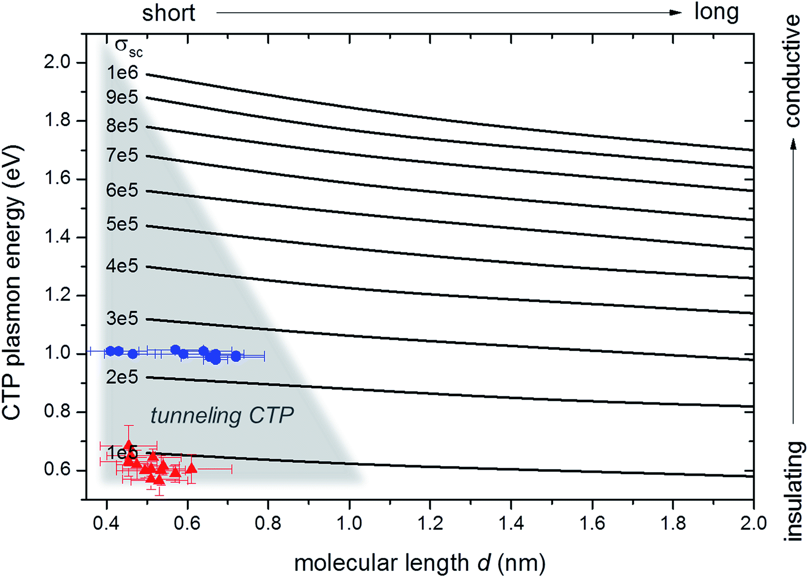 | ||
| Fig. 3 Constructed parameter map to correlate the resonant CTP plasmon energies ħωCTP (eV), the SAM conductivities σsc (S m−1), and the SAM molecular lengths d (nm) in the Ag–SAM–Ag system where the dimension of the Ag cubes is kept constant to 37 × 37 × 35 nm. The grey triangular area at the bottom left shows the quantum-tunneling-induced charge transfer plasmon regime (see also section “Charge injection mechanisms”), while the white area represents other kinds of CTP. Experimentally measured plasmon energies for two types of SAMs, i.e. EDT (1,2-ethanedithiolate, red triangles) and BDT (1,4-benzeneditiolate, blue circles) are shown on top of the theoretical database, which allows us to estimate their conductivities. The experimental data were taken from ref. 20. | ||
Charge injection mechanisms
Up to this point, for all the results shown above, the values of σsc (or nsc) are all assumed without considering any charge injection mechanism. It simply represents the value of nsc that is required to support a CTP mode at certain resonant energy, no matter what the charge injection mechanism is. To take into account various mechanisms, charge injection models must be developed to compute a charge-injection dependent σinj (or ninj). For example, for quantum-tunneling-enabled charge transfer plasmons, the charge injection modelling part will calculate a σtunnelinginj (or ntunnelinginj); if the tunneling-supplied ntunnelinginj meets the required nsc to support a CTP at a certain resonant energy, we can conclude that this CTP is a tCTP.Here, we develop a quantum-mechanical model to compute the tunneling charge-injection conductivity σtunnelinginj for the SAM with known molecular length d and Ag/SAM interface barrier height φ, by theoretically assuming a wide range of the extraction electric field E at the Ag/SAM interface. By doing so, we could estimate the required extraction electric field E to reach the space-charge limited tunneling regime for a particular type of SAM (i.e., defined by d and φ), similar to the approach used to model the Au–vacuum–Au systems.19,31
The quantum-tunneling charge injection at the Ag/SAM interface is modeled by the tunneling barrier profile Φ(x) of the Ag–SAM–Ag via the following five terms:19,20,29,31,34,35
| Φ(x) = φ + Φim(x) + Φv(x) + Φsc(x) + Φxc(x). | (4) |
The first term is the intrinsic barrier height φ at the interface of Ag and SAM (i.e., the energy level alignment of the molecular frontier orbitals of the SAMs and the Fermi-levels of the Ag electrode). This term φ is lower than the work function of the Ag electrode which serves as the barrier height in an Ag–vacuum–Ag system and it is tunable by changing SAMs. The second term is the image charge potential36 described by:
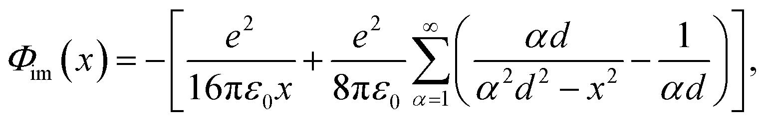 | (5) |
| Φv(x) = −eEx. | (6) |
The fourth term accounts for the self-induced space-charge field29,34,35 of the tunneling electrons Φsc(x). Lastly, the fifth term is the quantum exchange-correlation field Φxc(x). It is clear that the concept of space charge have already been incorporated into the tunneling charge injection process in the literature,29,31,34,35 indicating the applicability of the space-charge model in the modelling tCTP resonance.
The coupled Schrödinger and the Poisson equations are then solved iteratively using a WKB-type approximation technique34,35 for the tunneling barrier profile [illustrated by the red solid line in Fig. 4a] and the tunneling electron density ntunnelinginj. This ntunnelinginj can then be used to obtain the quantum tunneling charge-injection conductivity σtunnelinginj from eqn (2).
 | ||
| Fig. 4 (a) A schematic energy-level of the tunneling junction. For an intrinsic Ag–SAM–Ag junction (whose potential barrier is represented by the black dashed line), only term 1 (relevant to energy alignment of Ag and SAM) and term 2 (image charge potential) in eqn (4) are included: Φ(x) = φ + Φim(x). For an Ag–SAM–Ag junction subjected to a strong external field (whose potential barrier is represented by the red solid line), all five terms in eqn (4) are included Φ(x) = φ + Φim(x) + Φv(x) + Φsc(x) + Φxc(x), where the additional three come from the external field, the space charge field and exchange-correlation field. (b–d) Results of the quantum-calculations for three different molecular lengths d = (b) 0.5 nm, (c) 0.7 nm, and (d) 1.0 nm. Calculated tunneling conductivity σtunnelinginj (S m−1) values are plotted as a function of extraction electric field E (V m−1) for various intrinsic barrier heights φ (= 2, 3, 4 eV) at the Ag/SAM interface. | ||
This model automatically includes direct tunneling, Fowler-Nordheim tunneling, and over-the-barrier tunneling mechanisms. In addition, since only dimeric structures with a single layer of well-aligned SAMs are assumed in this theoretical study, there is no difference in modelling the through-space tunneling and through-bond tunneling mechanisms, unlike the cases for modelling the disordered or double layered SAMs.20
Fig. 4b–d shows the results of the quantum-calculations for three selected SAM molecular lengths d = 0.5, 0.7, and 1.0 nm, and a range of practical intrinsic barrier heights (2.0–4.0 eV). For comparison, the work function of Ag is 4.26 eV. The extraction electric field is theoretically varied from 107 to 1010 V m−1.
Take Fig. 4b (for all kinds of SAMs with the same molecular length d = 0.5 nm) as an example, we observe that for a large interface barrier height φ = 4 eV, the tunneling probability is low, we need the extraction field on the order of 109 V m−1 to enter into the space-charge limited tunneling regime. This observation agrees well to our previous studies on Au–vacuum–Au system.19 Such a high field makes it difficult to experimentally access. However, in this work, when the Ag–SAM–Ag system is proposed, the interface barrier height φ can be tuned to lower values like 2, 3 eV or even lower, and the required extraction field is greatly reduced to below 108 V m−1 as suggested by Fig. 4b. To compare the quantum-calculated σtunnelinginj with the values of detectable σsc (i.e., 105 to 106 S m−1) from our plasmon parameter map in Fig. 3, we draw a grey block in Fig. 4b, and all the data points falling in the grey block indicate the condition of the tCTP. We find that for all the 0.5 nm SAMs with barrier height up to 3.0 eV, the quantum tunneling CTP is feasible if the extraction electric field can be on the order of 108 V m−1.
Things are different for longer SAMs, for example, d = 0.7 nm as shown in Fig. 4c. As the tunneling distance is longer now, the tunneling probability decreases, leading to a strongly reduced overall tunneling conductivity. Even for a barrier height as low as 2.0 eV, the tunneling conductivity is estimated to be about 105 S m−1 only when the extraction field can be above 5 × 10⁸ V m−1 as shown in Fig. 4b. For even longer monolayer SAMs such as d = 1.0 nm as shown in Fig. 4d, following the same reasoning, the maximum tunneling conductivity for a range of practical intrinsic barrier heights can be on the order of 105 S m−1 only if the extraction field can reach to the level of a few 109 V m−1. These results imply that for smaller extraction fields, or longer SAM molecules, or larger interface barrier heights, the tunneling electrons that participate in the plasmonic oscillation is not enough.
Now, we refer back to our plasmon parameter map in Fig. 3. A grey triangle was drawn to indicate the quantum-tunneling-induced charge transfer plasmon regime assuming an extraction field of 109 V m−1. The regime of quantum-tunneling was found using the same approach as that used in Fig. 4, except that possible barrier heights are now allowed from 0.1 eV to infinite. It is observed that shorter SAMs (e.g., ∼0.4 nm) support a wider frequency range of tCTPs (0.6–2 eV), whereas longer SAMs (e.g., ∼1.0 nm) only support low-energy tCTPs (0.6 eV).
Measured data
We use here previously reported experimental data20 measured with monochromated electron energy-loss spectroscopy (EELS)37 to test our model. Junctions with two kinds of SAMs were used: (1) saturated, aliphatic 1,2-ethanedithiolate (EDT), and (2) aromatic 1,4-benzenedithiolate (BDT). The EDT (or BDT) molecules have an average molecular length of 0.55 ± 0.08 (or 0.67 ± 0.12) nm and a mean CTP plasmon energy of 0.60 ± 0.04 (or 1.01 ± 0.01) eV.The measured ħωCTP and d (only monolayer SAM junctions are selected) are plotted in red (EDT) and blue (BDT) in Fig. 3, respectively. From Fig. 3, we can readily infer the conductivity of the SAM: σEDT ≈ 1.0 × 10⁵ S m−1, giving an equivalent conductance GEDT = σEDT(A/dEDT) = 3221G0 for the 0.55 nm-thick EDT layer; whereas σBDT ≈ 2.5 × 10⁵ S m−1, with equivalent conductance GBDT = σBDT(A/dBDT) = 6611G0 for the 0.67 nm-thick BDT layer. Here G0 = 2e2/h = 7.727 × 10⁻⁵ S is the quantum conductance.
It is now instructive to estimate the electric field in the gap in our EELS experiments to check whether the conditions of tunneling can be met. To the best of our knowledge, there is no direct method to measure the electric field associated with the incident electron beam. Instead, we employed a widely used LC circuit model.2,38 We noticed from our calculations in Fig. 2 that our measured EDT (σEDT ≈ 1.0 × 10⁵ S m−1) and BDT (σBDT ≈ 2.5 × 10⁵ S m−1) belong to the moderate conductivity regime. For such junctions, both CTP and BDP are supported (Fig. 2a) and the gap field is enhanced at CTP resonances (Fig. 2c). Therefore the Ag–EDT–Ag and Ag–BDT–Ag junctions can be modeled as capacitors.2,38 We could estimate the average electric field in the gap based on the energy of a single plasmon using 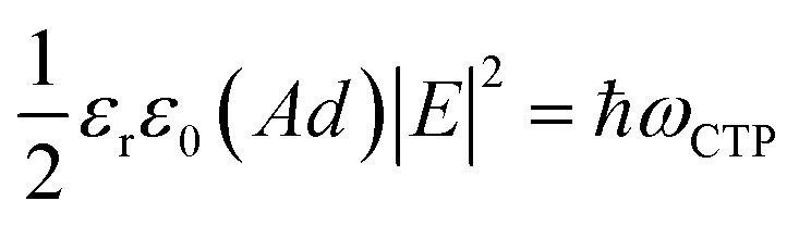 at the CTP resonance. Here A is the area of overlap of the two plates, εr is the relative static permittivity of the material between the plates, ε0 is the vacuum permittivity, and d is the separation between the plates. Therefore the average field in the gap is
  , which is computed to be on the order of 108 V m−1 at the CTP resonance. For comparison, the values of plasmonic fields determined in molecular junctions by current rectification at optical frequencies are about 109 V m−1.39
Our estimated field on the order of 108 V m−1 is not able to reach the Fowler–Nordheim tunneling regime for an Au–vacuum–Au dimer in our previously study19 due to the large intrinsic barrier height defined by the work function of Au (where it is found that 1010 V m−1 is required19). However, we have shown in our Fig. 4 that the average gap field on the order of 108 V m−1 is enough to induce Fowler–Nordheim tunneling for some Ag–SAM–Ag systems studied in this work, because now the intrinsic barrier is greatly lowered.
Let us take a close look at Fig. 4b for SAM of 0.5 nm thickness again, for the practical range of intrinsic barrier heights (1–3 eV), and the possible range of extraction electric field (107 to 5 × 10⁸ V m−1) in our EELS experiments, the calculated tunneling induced conductivity is indeed on the order of 105 S m−1. This is a clear indication that tCTP is one of the possible ways to explain what we have observed experimentally.20
From the previously reported surface coverage of 8.0 × 10⁻¹⁰ mol cm−2 for these molecules on silver surfaces,40,41 we estimate that 16000 molecules are present in the 37 × 37 nm2 junction of each silver dimer. Therefore, the conductance per EDT or BDT molecule is roughly 0.2G0 and 0.4G0 at the CTP resonance (140 THz and 245 THz), respectively, assuming that every molecule participates in charge transport. It is found that these THz conductance values per molecule happen to be of the same order as those previous experimentally obtained values in break junction measurement at dc and low-frequencies.42,43 Despite the similar conductivity values, the differences between our experiments and the referenced experiments42,43 should be taken note: (I) ours is molecular monolayer junction whereas the referenced experiments are single-molecule junctions. They are clearly different transport junctions.26. (II) The shapes of the electrodes in both test beds are vastly different. (III) The measurement frequencies are different. Very recent work on an atomic-scale plasmonic switch44 also suggested that a single atom can open a conductive tunneling channel with a conductance in the order of 0.13G0.
It is interesting to note that the two types of molecules we have chosen for our proof-of-concept experiment (EDT and BDT) both fall within the tunneling CTP regime of Fig. 3. They have quite similar molecular lengths (the difference is only 0.1 nm), but rather different CTP plasmon energy (the difference is about 0.4 eV). This is a piece of clear experimental evidence that CTP plasmon energy not only depends on junction geometry, but also on junction conductivity. We propose further experimental investigations for different SAMs and other gap dielectrics to further explore the tunneling and other charge transport regimes.
Conclusions
In conclusion, we have established a framework for measuring the conductance of single molecules at near-infrared, THz frequencies by utilizing the charge transfer plasmon resonances in hybrid Ag–molecule–Ag dimer systems. This measurement is based on the unique feature of charge transfer plasmons: their energies are sensitive to the electrical properties of the molecular junction. A wide range of molecules was theoretically explored to construct a charge transfer plasmon parameter map using a generalized space-charge corrected electromagnetic model.The space-charge corrected electromagnetic model developed in this work treats the charge injection and charge transport separately. A Drude expression (assuming damping frequency on the order of driving frequency) is used to model the dynamics of the space-charge limited charge transport, whereas the charge injection modelling takes care of the number density of the transporting charges. It should be noted that this space-charge corrected electromagnetic model is only appropriate to model the space-charge limited charge transport problem.
In particular, the space-charge limited quantum-tunneling charge transport problem is attempted. The space-charge limited regime (i.e., small gap spacing, low interface barrier height, and large gap field) is found, and the molecules that are able to support space-charge limited quantum-tunneling charge transfer plasmons under certain extraction electric fields are identified.
To demonstrate the feasibility of the proposed framework, previously reported experimental results from two types of molecules were analyzed: saturated, aliphatic 1,2-ethanedithiolate (EDT), and aromatic 1,4-benzenedithiolate (BDT). The measured conductance per EDT or BDT molecule is respectively 0.2G0 (at 140 THz) and 0.4G0 (at 245 THz). Both molecules likely support the space-charge limited tunneling charge transfer plasmons, based on the comparable magnitude between our theoretically-predicted required junction field (for given molecular length and barrier height) and the estimated junction field in our EELS measurement.
Our study suggests a direction for future experimental investigations, e.g., using different molecules that support other types of charge transport mechanisms. This would further refine the map shown in Fig. 3, providing a complete and comprehensive charge transport picture in the THz frequency domain.
Acknowledgements
We acknowledge the National Research Foundation (NRF) for supporting this research under the Competitive Research Programme (CRP) program (award NRF-CRP 8-2011-07). This research is supported by the National Research Foundation; Prime Minister's Office, Singapore, under its Medium sized Centre Programme. J. K. W. Y, P. B., and L. W. acknowledge the Agency for Science, Technology and Research (A*STAR) for the A*STAR Investigatorship Grant, and TSRP grant 1021520014.References
- M. Hentschel, L. Wu, M. Schäferling, P. Bai, E. P. Li and H. Giessen, Optical properties of chiral three-dimensional plasmonic oligomers at the onset of charge-transfer plasmons, ACS Nano, 2012, 6, 10355–10365 CrossRef CAS PubMed.
- H. Duan, A. I. Fernández-Domínguez, M. Bosman, S. Maier and J. K. W. Yang, Nanoplasmonics: classical down to the nanometer scale, Nano Lett., 2012, 12, 1683–1689 CrossRef CAS PubMed.
- L. Wu, P. Bai and E. P. Li, Designing surface plasmon resonance of subwavelength hole arrays by studying absorption, J. Opt. Soc. Am. B, 2012, 29, 521–528 CrossRef CAS.
- Y. Huang, L. Wu, X. Chen, P. Bai and D.-H. Kim, Synthesis of anisotropic concave gold nanocuboids with distinctive plasmonic properties, Chem. Mater., 2013, 25, 2470–2475 CrossRef CAS.
- S. Sun, H. Liu, L. Wu, C. E. Png and P. Bai, Interference induced broadband absorption enhancement for plasmonic-metal@semiconductor microsphere as visible light photocatalyst, ACS Catal., 2014, 4, 4269–4276 CrossRef CAS.
- Y. Wang, L. Wu, X. Zhou, T. I. Wong, J. Zhang, P. Bai, E. P. Li and B. Liedberg, Incident-angle dependence of fluorescence enhancement and biomarker immunoassay on gold nanohole array, Sens. Actuators, B, 2013, 186, 205–211 CrossRef CAS.
- T. I. Wong, S. Han, L. Wu, Y. Wang, J. Deng, C. Y. L. Tan, P. Bai, Y. C. Loke, X. D. Yang, M. S. Tse, S. H. Ng and X. Zhou, High throughput and high yield nanofabrication of precisely designed gold nanohole arrays for fluorescence enhanced detection of biomarkers, Lab Chip, 2013, 13, 2405–2413 RSC.
- H. Y. Song, T. I. Wong, A. Sadovoy, L. Wu, P. Bai, J. Deng, S. Guo, Y. Wang, W. Knoll and X. Zhou, Imprinted gold 2D nanoarray for highly sensitive and convenient PSA detection via plasmon excited quantum dots, Lab Chip, 2015, 15, 253–263 RSC.
- T. Atay, J. H. Song and A. V. Nurmikko, Strongly interacting plasmon nanoparticle pairs: from dipole−dipole interaction to conductively coupled regime, Nano Lett., 2004, 4, 1627–1631 CrossRef CAS.
- I. Romero, J. Aizpurua, G. W. Bryant and F. J. G. De Abajo, Plasmons in nearly touching metallic nanoparticles: singular response in the limit of touching dimers, Opt. Express, 2006, 14, 9988–9999 CrossRef PubMed.
- J. B. Lassiter, J. Aizpurua, L. I. Hernandez, D. W. Brandl, I. Romero, S. Lal, J. H. Hafner, P. Nordlander and N. J. Halas, Close encounters between two nanoshells, Nano Lett., 2008, 8, 1212–1218 CrossRef CAS PubMed.
- M. Schnell, A. García-Etxarri, A. J. Huber, K. Crozier, J. Aizpurua and R. Hillenbrand, Controlling the near-field oscillations of loaded plasmonic nanoantennas, Nat. Photonics, 2009, 3, 287–291 CrossRef CAS.
- J. Zuloaga, E. Prodan and P. Nordlander, Quantum description of the plasmon resonances of a nanoparticle dimer, Nano Lett., 2009, 9, 887–891 CrossRef CAS PubMed.
- N. Large, M. Abb, J. Aizpurua and O. L. Muskens, Photoconductively loaded plasmonic nanoantenna as building block for ultracompact optical switches, Nano Lett., 2010, 10, 1741–1746 CrossRef CAS PubMed.
- O. Pérez-González, N. Zabala, A. G. Borisov, N. J. Halas, P. Nordlander and J. Aizpurua, Optical spectroscopy of conductive junctions in plasmonic cavities, Nano Lett., 2010, 10, 3090–3095 CrossRef PubMed.
- D. C. Marinica, A. K. Kazansky, P. Nordlander, J. Aizpurua and A. G. Borisov, Quantum plasmonics: nonlinear effects in the field enhancement of a plasmonic nanoparticle dimer, Nano Lett., 2012, 12, 1333–1339 CrossRef CAS PubMed.
- R. Esteban, A. G. Borisov, P. Nordlander and J. Aizpurua, Bridging quantum and classical plasmonics with a quantum-corrected model, Nat. Commun., 2012, 3, 825 CrossRef PubMed.
- K. J. Savage, M. M. Hawkeye, R. Esteban, A. G. Borisov, J. Aizpurua and J. J. Baumberg, Revealing the quantum regime in tunneling plasmonics, Nature, 2012, 491, 574–577 CrossRef CAS PubMed.
- L. Wu, H. Duan, P. Bai, M. Bosman, J. K. W. Yang and E. P. Li, Fowler–Nordheim tunneling induced charge transfer plasmons between nearly touching nanoparticles, ACS Nano, 2013, 7, 707–716 CrossRef CAS PubMed.
- S. F. Tan, L. Wu, J. K. W. Yang, P. Bai, M. Bosman and C. A. Nijhuis, Quantum plasmon resonances controlled by molecular tunnel junctions, Science, 2014, 343, 1496–1499 CrossRef CAS PubMed.
- F. Wen, Y. Zhang, S. Gottheim, N. S. King, Y. Zhang, P. Nordlander and N. J. Halas, Charge transfer plasmons: optical frequency conductances and tunable infrared resonances, ACS Nano, 2015, 9, 6428–6435 CrossRef CAS PubMed.
- R. Esteban, G. Aguirregabiria, A. G. Borisov, Y. M. Wang, P. Nordlander, G. W. Bryant and J. Aizpurua, The morphology of narrow gaps modifies the plasmonic response, ACS Photonics, 2015, 2, 295–305 CrossRef CAS.
- R. Esteban, A. Zugarramurdi, P. Zhang, P. Nordlander, F. J. García-Vidal, A. G. Borisov and J. Aizpurua, A classical treatment of optical tunneling in plasmonic gaps: extending the quantum corrected model to practical situations, Faraday Discuss., 2015, 178, 151–183 RSC.
- U. Hohenester, Quantum corrected model for plasmonic nanoparticles: A boundary element method implementation, Phys. Rev. B: Condens. Matter Mater. Phys., 2015, 91, 205436 CrossRef.
- F. Benz, C. Tserkezis, L. O. Herrmann, B. de Nijs, A. Sanders, D. O. Sigle, L. Pukenas, S. D. Evans, J. Aizpurua and J. J. Baumberg, Nanooptics of molecular-shunted plasmonic nanojunctions, Nano Lett., 2015, 15, 669–674 CrossRef CAS PubMed.
- A. Nitzan and M. A. Ratner, Electron transport in molecular wire junctions, Science, 2003, 300, 1384–1389 CrossRef CAS PubMed.
- C. Joachim and M. A. Ratner, Molecular electronics: some views on transport junctions and beyond, Proc. Natl. Acad. Sci. U. S. A., 2005, 102, 8801–8808 CrossRef CAS PubMed.
- C. D. Child, Discharge from hot CaO, Phys. Rev., 1911, 32, 492–511 CAS.
- L. K. Ang, T. J. T. Kwan and Y. Y. Lau, New scaling of Child-Langmuir law in the quantum regime, Phys. Rev. Lett., 2003, 91, 208303 CrossRef CAS PubMed.
- S. A. Maier, Plasmonics: fundamentals and applications, Springer, 2007 Search PubMed.
- P. Zhang, Scaling for quantum tunneling current in nano- and subnano-scale plasmonic junctions, Sci. Rep., 2015, 5, 9826 CrossRef CAS PubMed.
- P. M. Kraus, B. Mignolet, D. Baykusheva, A. Rupenyan, L. Horný, E. F. Penka, G. Grassi, O. I. Tolstikhin, J. Schneider, F. Jensen, L. B. Madsen, A. D. Bandrauk, F. Remacle and H. J. Wörner, Measurement and laser control of attosecond charge migration in ionized iodoacetylene, Science, 2015, 350, 790–795 CrossRef CAS PubMed.
- E. D. Palik, Handbook of optical constants of solids, Academic, San Diego, Calif, 1991 Search PubMed.
- L. Wu, L. K. Ang and W. S. Koh, Theory of shot noise in high-current space-charge-limited field emission, Phys. Rev. B: Condens. Matter Mater. Phys., 2008, 77, 115351 CrossRef.
- L. Wu and L. K. Ang, Nonequilibrium model of ultrafast laser-induced electron photofield emission from a dc-biased metallic surface, Phys. Rev. B: Condens. Matter Mater. Phys., 2008, 78, 224112 CrossRef.
- N. W. Ashcroft and N. D. Mermin, Solid State Physics, Saunders, 1976 Search PubMed.
- M. Bosman, V. J. Keast, M. Watanabe, A. I. Maaroof and M. B. Cortie, Mapping surface plasmons at the nanometer scale with an electron beam, Nanotechnology, 2007, 18, 165505 CrossRef.
- D. Zhu, M. Bosman and J. K. Yang, A circuit model for plasmonic resonators, Opt. Express, 2014, 22(8), 9809–9819 CrossRef CAS PubMed.
- R. Arielly, A. Ofarim, G. Noy and Y. Selzer, Accurate determination of plasmonic fields in molecular junctions by current rectification at optical frequencies, Nano Lett., 2011, 11, 2968–2972 CrossRef CAS PubMed.
- H. Sellers, A. Ulman, Y. Shnidman and J. E. Eilers, Structure and binding of alkanethiolates on gold and silver surfaces: implications for self-assembled monolayers, J. Am. Chem. Soc., 1993, 115, 9389–9401 CrossRef CAS.
- E. G. Cox, D. W. J. Cruickshank and J. A. S. Smith, The crystal structure of benzene at −3 °C, Proc. R. Soc. London, Ser. A, 1958, 247, 1–21 CrossRef CAS.
- Y. Kim, T. Pietsch, A. Erbe, W. Belzig and E. Scheer, Benzenedithiol: A broad-range single-channel molecular conductor, Nano Lett., 2011, 11, 3734–3738 CrossRef CAS PubMed.
- M. Kiguchi, N. Sekiguchi and K. Murakoshi, In situ preparation of a single molecular junction with mechanically controllable break junctions in vacuum, J. Phys.: Conf. Ser., 2008, 100, 052059 CrossRef.
- A. Emboras, J. Niegemann, P. Ma, C. Haffner, A. Pedersen, M. Luisier, C. Hafner, T. Schimmel and J. Leuthold, Atomic scale plasmonic switch, Nano Lett., 2016, 16(1), 709–714 CrossRef CAS PubMed.
| This journal is © The Royal Society of Chemistry 2016 |