
Silicene and graphene nano materials in gas sensing mechanism
Elnaz Akbaria,
Zolkafle Buntat*a,
Abdolkarim Afroozehb,
Seyed Ebrahim Pourmandc,
Yousef Farhangd and
Parisa Sanatie
aInstitute of High Voltage & High Current, Faculty of Electrical Engineering, Universiti Teknologi Malaysia, Johor Bahru, 81310 Malaysia. E-mail: zolkafle@utm.my
bYoung Researchers and Elite Club, Jahrom Branch, Islamic Azad University, Jahrom, Iran
cDepartment of Optics and Lasers Engineering, Islamic Azad University, Estahban Branch, Estahban, Iran
dFaculty of Computer, Islamic Azad University, Khoy Branch, Khoy, Iran
eInstitute of Bioproduct Development (IBD), Universiti Teknologi Malaysia, Johor Bahru, Johor, Malaysia
First published on 10th August 2016
Abstract
Silicene, the Si analogue of graphene, has recently extended the short list of existing two-dimensional (2D) atomic crystals. There are many remarkable electrical properties as well as unique thermal conductivities associated with graphene and silicene making them perfect materials that possess great potential to replace and provide an even better performance than silicon in future generation semiconductor devices. It is expected that novel devices developed with these will be much faster and smaller in size than their contemporary counterparts. Although graphene and silicene display different electrical conductivity behavior, their carrier concentration has similar behavior. The current–voltage characteristics of silicene/graphene field effect transistors (FETs) have been demonstrated at different operating temperatures under the flow of different NH3 gas concentrations. It was found that in similar conditions, the suggested model for a gas sensor based on graphene shows higher electrical conductivity compared to silicene.
1. Introduction
Graphene is a two-dimensional structure of sp2 hybridized carbon atoms arranged in a hexagonal structure having intriguing properties such as high mobility and high conductivity. Graphene has shown its potentiality to be an essential part of many future electronic circuits and devices utilized in high frequency and logic transistors and switches.1–3 Its structural and electrical properties make it a promising candidate, as the valence and conduction bands are separated by a zero band gap. The zero band gap features of graphene and its property to exhibit a large electric field effect allow doping with electrons or holes through electrostatic gating.4 The zero band gap limits the digital applications, but the high mobility compensates for it and draws attention to use for high frequency devices.8,9 Carrier mobilities ranging from around 500 to 20![[thin space (1/6-em)]](https://www.rsc.org/images/entities/char_2009.gif) 000 cm2 V−1 s−1 have been previously reported for single, double and tri-layer graphene films.5 Electrically contacted suspended graphene films have been reported to achieve a tenfold improvement in the mobilities exceeding 200000 cm2 V−1 s−1.6,10 The unusually high carrier mobility promises a fast operating speed for graphene transistors.7 Apart from high carrier mobilities, graphene-based thin film transistors (TFTs) also exhibit large critical current densities. Therefore, graphene can be used an outstanding alternative to the miniaturization of electronic systems and devices.11
000 cm2 V−1 s−1 have been previously reported for single, double and tri-layer graphene films.5 Electrically contacted suspended graphene films have been reported to achieve a tenfold improvement in the mobilities exceeding 200000 cm2 V−1 s−1.6,10 The unusually high carrier mobility promises a fast operating speed for graphene transistors.7 Apart from high carrier mobilities, graphene-based thin film transistors (TFTs) also exhibit large critical current densities. Therefore, graphene can be used an outstanding alternative to the miniaturization of electronic systems and devices.11
Silicene,12 the Si analogue of graphene, has recently been synthesized in the form of nanoribbons,13 pristine14,15 and Mg-doped sheets on substrates and free-standing Si multilayers. Unlike graphene, silicene prefers a low-buckled structure.16–18 Moreover, pristine silicene is a zero-gap semi-metal with Dirac cones as observed in graphene. With the nearly massless Dirac fermion character, high carrier mobility is expected in silicene. It makes silicene an attractive material for high-speed electronic devices. When silicene is used as the channel, the silicene-based transistor will own an ultrafast speed, making it able to operate in the THz frequency range.19 Apparently, the pristine silicene cannot be used directly in FETs due to its zero band gap. Thus, opening the Eg without degrading its electronic characteristics is equally extremely desirable for its electronic applications. Considerable attempts have been made to open Eg of silicene. From the standpoint of whether the integrity of the honeycomb structure is maintained, there are two main types of approach. One mainly involves chemical functionalization,20 cutting silicene into nanoribbons,21 adsorption or absorption adatoms,22 making defects in silicene,23 which inevitably damages the structure, thus the carrier mobility would significantly reduce. The other approach mainly adopts an external electric field24 or non-covalent silicene–substrate interaction.25 Graphene is a zero-gap semiconductor with sp2 hybridization. Silicene is similar to graphene but supports a mixture of sp2 and sp3 hybridizations. As a consequence, silicene has a buckled structure, see Fig. 1.
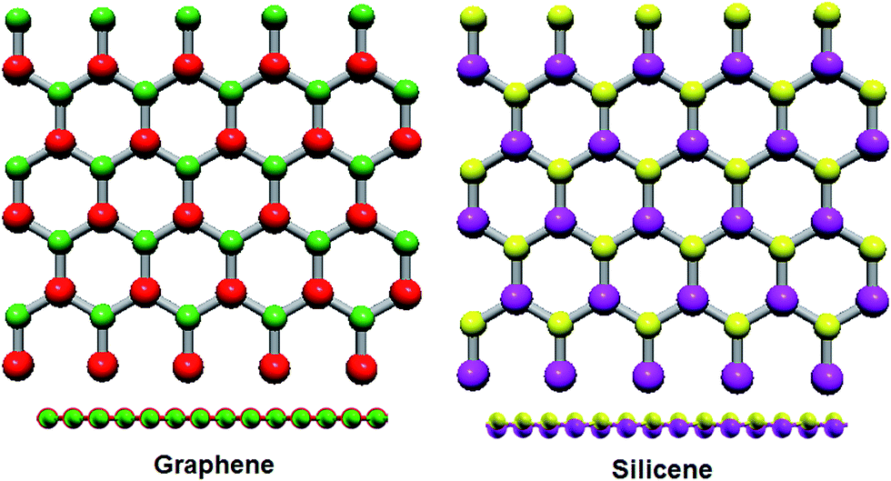 | ||
| Fig. 1 Schematic structure of graphene and silicene. | ||
Silicene is expected to have similar electronic properties as graphene and hence, could lead to similar applications. The structural parameters for graphene and silicene are summarized in Table 1.
| System | Band gap (meV) | Bond length (Å) | Lattice constant (Å) |
|---|---|---|---|
| Graphene | — | 1.42 | 2.46 |
| Silicene | 2.00 | 2.24 | 3.86 |
Gases such as CO, O2, H2, NO, NO2, and CO2 need to be closely monitored to prevent air pollution, health hazards, and device contamination. To this end, it is important to create new low-dimension sensors with high sensitivity, selectivity and recoverability. The emergence of high surface area nanomaterials has led to enhanced gas detection capabilities at finer resolutions.26 Despite recent advances, reliably detecting, identifying, and releasing a single gas molecule has remained an elusive task. Notable progress has already been made towards realizing graphene-based NH3 nanosensors. However, pristine graphene nanoribbons have been found to be electronically sensitive to NH3 adsorptions and thus detectable conductance modulation. Some groups have noted that the experimentally realized sensing ability of graphene27 must rely heavily on oxygen functionalization, substrate effects and high defect concentrations.28 Further studies have explored doping and functionalization of graphene to strengthen the NH3–graphene interaction and enhance conduction modulation.29 Silicene, the silicon equivalent of graphene, has been shown to interact more strongly with foreign molecules and atoms compared to graphene. Previous works have shown that molecular and atomic adsorptions30,31 and doping32,33 can significantly modify the electronic properties of silicene sheets. This stronger interaction (compared to graphene) can be explained by the lack of a stable sp2 form of silicene, i.e. silicene prefers complete sp3 hybridization, which is made possible by various gas adsorptions. A major limitation of monolayer silicene is that it is highly reactive towards atmospheric gases; therefore, silicene has to be deposited over metal substrates that alter their electronic properties due to strong metal–Si covalent bonds. One easy route to obtain almost pristine silicene is to use the 100 layer of CaSi2 where independent silicene layers exists and are only weakly coordinated with Ca(II).34
2. FET-based sensor
A novel generation of gas sensors has currently appeared with the arrival of semiconductor nanowires. Due to the low dimensions of these materials, the charge carrier concentrations that are attributed to adsorbed gas molecules can result in detectable signals. The normal way to do this is by making use of these nanomaterials in a field effect transistor (FET) device35,36 in which the adsorbing molecules play the part of gate voltage.A recent study on graphene/silicene-based gas sensors has demonstrated that the change in conductance of graphene/silicene is due to enhancement of electron mobility combined with the effect of direct charge transfer from the adsorbed gas species. In this study, we have employed graphene/silicene nanoribbon in FET37–41 sensor devices to detect NH3 gas. The FET structure of an NH3 gas sensor set-up is depicted in Fig. 2.
 | ||
| Fig. 2 Schematic of a FET NH3 gas sensor. | ||
It has been demonstrated that graphene is capable of detecting individual gas molecules due to its low noise.42 The sensing mechanism of graphene has been explained in terms of chemical doping, which is a direct result of the gas species (being adsorbed on the surface of graphene) acting either as donors or acceptors,43,44 consequently changing the charge carrier concentration in graphene and its conductivity accordingly. In this study, the conductance of a graphene-based sensor and a silicene-based sensor has been compared.
The band structure of materials is the starting point to investigate their electrical properties. The band structure of silicene is shown in eqn (1):45,46
 | (1) |
 is the K vector and νF = 1.3 × 10⁶ m s−1 is the Fermi velocity.
The electron transport for silicene has been assumed to be ballistic and by using Landauer's formula, the electrical conductance can be calculated as shown in eqn (2):
 | (2) |
 | (3) |
This has considered the conductance in the presence of an external perpendicular electric field. By combination of Landauer's formula and the number of modes, the conductance of silicene can be indicated as in eqn (4) below:45
 | (4) |
By changing variables, simplifying and using partial integration techniques, eqn (4) could be obtained as eqn (5), which shows the general electrical conductivity of silicene as a two-dimensional channel in the silicene-based FET:
 | (5) |
It has been demonstrated that when the silicene-based sensor is under ammonia gas exposure, the electrical conductivity will be changed.47 In eqn (6), the proposed model is presented that shows the relation between electrical conductivity, NH3 concentration and temperature:48
| σwith gas = σwithout gas + σwith gas(T) + σwith gas(F) | (6) |
For the silicene gas sensor, in altered temperatures and under the gas exposure, three parameters for electrical conductivity can be defined as σwgT, σwog, and σwgF. The first parameter, σwgT is the conductance variation depending on T, σwog is assumed as the conductivity without gas exposure and σwgF is defined as gas concentration variation.49 It has been shown that when the silicene sensor is under ammonia gas exposure, the electrical conductivity is changed according to different gas concentrations and temperatures. The Eg parameter results in conductance variation of the channel. It has been depicted that the Eg parameter is dependent on gas concentration and temperature. Therefore, we can write
 | (7) |
Lastly, to obtain the electrical conductance, model eqn (5) and (7) are employed as
 | (8) |
 | (9) |
 | (10) |
where ζ(n) is defined as the Riemann zeta function, from eqn (10), and by assuming the degenerate limit (ηF ≫ 0), the Fermi integral can be obtained as follows:

| Fj(ηF) → ηFj+1/Γ(j + 2) | (11) |
By simplifying eqn (10), the Fermi–Dirac integral function of order 1 can be written as in eqn (12) below:51
 | (12) |
Through eqn (13), the I–V characteristic of the graphene/silicene-based FET can be measured. It has been assumed that the substrate terminals and source are held in ground potential. A flow of electrons appears in the channel region by applied voltage between drain-to-source (VDS). Furthermore, by using the Fermi integral and the relationship between conductance and current the I–V equation of silicene can be obtained as in eqn (13) below:
 | (13) |
The use of the graphene-based FET (GFET) for gas sensing may be greatly appreciated due to its integration capability in electronic devices because graphene is emerging as a potential candidate in field effect devices with very high carrier mobility. Very few researchers have reported the gas sensing behavior of GFET devices for the detection of NH3 at ppm levels.52 Lu et al.53 and Romero et al.54 performed the experimental study for high concentrations of NH3 (1–5%) sensing by GFET at room temperature under high vacuum conditions. The flow of electrons between the drain and source is the fundamental operational principle in MOSFET.
Regarding the Landauer formula, there is a relationship between the transmission probability through the electrodes and σ, which can be written as eqn (14):55
 | (14) |
 | (15) |
 | (16) |
It has been presented that electrical conductivity variation occurs when graphene is under ammonia gas exposure.58
 | (17) |
3. Results and discussion
In order to fully characterize a graphene FET, a variety of electrical measurements have to be conducted to evaluate the functionality of the device. The most important measurement to be taken is the source-drain current as a function of a varying gate voltage (IDS-VGS curve of the device). One can draw many conclusions from these results, such as the position of the Dirac point, the mobility of the electrons and the carrier concentrations as a function of the applied gate voltage. Fig. 3a–c demonstrates the current–voltage characteristics of the graphene/silicene nanostructures corresponding to different NH3 concentrations (100 ppm, 200 ppm and 500 ppm) and the I–V plot depicting an increase in current with increasing NH3 carrier concentration. | ||
| Fig. 3 I–V characteristics of silicene and graphene at T = 200 °C and different carrier concentrations. | ||
Fig. 4 illustrates the I–V characteristics of silicene and graphene gas sensors when they are exposed under a concentration of 500 ppm NH3 and different temperatures.58
 | ||
| Fig. 4 Current–voltage characteristics of silicene and graphene at different temperatures under NH3 gas exposure at a concentration of F = 500 ppm. | ||
The interactions of ammonia molecules with the surface of silicene/graphene can be detected by measuring the changes in conductivity arising from charge transfer or changes in electron mobility. The charge transfer can occur through the interaction with graphene of either electron-donating or electron-withdrawing gas molecules leading to a change in carrier concentration. Some gas molecules can dope graphene with electrons, while others can dope graphene with holes. The interactions of ammonia molecules with the surface atoms of silicene/graphene can range from weaker van der Waals' to strong covalent bonding depending on the adsorbate. It can be seen from the plots that the measured current–voltage characteristics increase with increased temperature and it has been demonstrated that electrical conductance of graphene is generally larger than that of silicene.
As shown in Table 2, two parameters α and β for different values of temperature and NH3 concentration have been defined.
| Temperature (°C) | NH3 concentration (ppm) | α | β |
|---|---|---|---|
| 200 | 100 | −0.46 | 0.013 |
| 200 | 200 | −0.46 | 0.018 |
| 200 | 500 | −0.46 | 0.025 |
| 25 | 500 | −3.6 | 0.025 |
| 50 | 500 | −2.7 | 0.025 |
| 100 | 500 | −1.2 | 0.025 |
| 150 | 500 | −0.6 | 0.025 |
Regarding the suggested models, α and β have been defined as the control parameters that have been calculated by the iteration method. In this study, the proposed model demonstrated that the rate of electrical conductance depends on temperature and can be obtained from
| α = mln(T) − n |
Moreover, gas concentration has been introduced by the β parameter, which is measured by the iterative method β = xln(F) − z and has shown that the conductance variation is related to NH3 gas concentration with x = 1.03 and z = 7.54.
4. Conclusion
Being comprised mainly surface atoms within its 2D structure, silicene/graphene's exceptional properties make it an excellent candidate for chemical sensing applications. The high surface-to-volume ratio combined with their excellent electrical, optical, and mechanical properties has led researchers to explore incorporating graphene into various chemical, electronic, biological, mechanical, and optoelectronic sensors. In this study, for the gas sensing behavior, a FET-based approach has been employed to study the adsorption behavior of ammonia (NH3) on the graphene/silicene surfaces, and α and β have been defined as temperature and NH3 concentration control parameters, respectively. Silicene and graphene have been used in the structure of a FET gas sensor. These materials have been used as an example to obtain a detailed understanding of computational procedures and allow a comparison with previous experimental studies in order to check the correctness of our calculation method. The current–voltage characteristics have been calculated under different temperatures and NH3 gas concentrations and it is obvious that electrical conductance of graphene is higher than that of silicene.Acknowledgements
The authors would like to thank the Ministry of Education (MOE), Malaysia (grant Vot. No. 4F382) and the Universiti Teknologi Malaysia (GUP grant Vot. No. 07H56 and Post-Doc grant Vot. No. 02E87) for the financial support received during the investigation.References
- E. Akbari, et al., Gas concentration effects on the sensing properties of bilayer graphene, Plasmonics, 2014, 9(4), 987–992 CrossRef CAS.
- A. C. Neto, et al., The electronic properties of graphene, Rev. Mod. Phys., 2009, 81(1), 109 CrossRef.
- E. Akbari, et al., Sensing and identification of carbon monoxide using carbon films fabricated by methane arc discharge decomposition technique, Nanoscale Res. Lett., 2014, 9(1), 1 CrossRef CAS PubMed.
- M. F. Khan, M. Z. Iqbal, M. W. Iqbal and J. Eom, Improving the electrical properties of graphene layers by chemical doping, Sci. Technol. Adv. Mater., 2014, 15(5), 055004 CrossRef.
- A. C. Ferrari, et al., Science and technology roadmap for graphene, related two-dimensional crystals, and hybrid systems, Nanoscale, 2015, 7(11), 4598–4810 RSC.
- K. I. Bolotin, et al., Ultrahigh electron mobility in suspended graphene, Solid State Commun., 2008, 146(9), 351–355 CrossRef CAS.
- N. O. Weiss, et al., Graphene: an emerging electronic material, Adv. Mater., 2012, 24(43), 5782–5825 CrossRef CAS PubMed.
- J. Park, et al., Transfer-free batch fabrication of single layer graphene devices, US Pat., Application No. 13/384,663, 2010.
- B. M. Blaschke, et al., Flexible graphene transistors for recording cell action potentials, 2D Materials, 2016, 3(2), 025007 CrossRef.
- W. Zhu, et al., Silicon nitride gate dielectrics and band gap engineering in graphene layers, Nano Lett., 2010, 10(9), 3572–3576 CrossRef CAS PubMed.
- M. Kim, et al., Improvement of carrier mobility of top-gated SiC epitaxial graphene transistors using a PVA dielectric buffer layer, Nanotechnology, 2012, 23(33), 335202 CrossRef PubMed.
- M. Kanno, et al., Electronic decoupling by h-BN layer between silicene and Cu(111): a DFT-based analysis, New J. Phys., 2014, 16(10), 105019 CrossRef.
- S. M. Aghaei and I. Calizo, Band gap tuning of armchair silicene nanoribbons using periodic hexagonal holes, J. Appl. Phys., 2015, 118(10), 104304 CrossRef.
- T. Kaloni, et al., Current developments in silicene and germanene, Phys. Status Solidi RRL, 2016, 10(2), 133–142 CrossRef CAS.
- Y. Guo, et al., Tunable thermal conductivity of silicene by germanium doping, J. Supercond. Novel Magn., 2016, 29(3), 717–720 CrossRef CAS.
- D. Jose and A. Datta, Understanding of the buckling distortions in silicene, J. Phys. Chem. C, 2012, 116(46), 24639–24648 CAS.
- D. Jose, A. Nijamudheen and A. Datta, Tip enhanced Raman spectroscopy (TERS) as a probe for the buckling distortion in silicene, Phys. Chem. Chem. Phys., 2013, 15(22), 8700–8704 RSC.
- A. Nijamudheen, et al., Electronic and chemical properties of germanene: the crucial role of buckling, J. Phys. Chem. C, 2015, 119(7), 3802–3809 CAS.
- Z. Ni, et al., Tunable band gap and doping type in silicene by surface adsorption: towards tunneling transistors, Nanoscale, 2014, 6(13), 7609–7618 RSC.
- B. Huang, H. Xiang and S.-H. Wei, Chemical Functionalization of Silicene: Spontaneous Structural Transition and Exotic Electronic Properties, Phys. Rev. Lett., 2013, 111(14), 145502 CrossRef PubMed.
- P. De Padova, et al., sp2-like hybridization of silicon valence orbitals in silicene nanoribbons, Appl. Phys. Lett., 2011, 98(8), 081909 CrossRef.
- J. Sivek, et al., Adsorption and absorption of boron, nitrogen, aluminum, and phosphorus on silicene: stability and electronic and phonon properties, Phys. Rev. B: Condens. Matter Mater. Phys., 2013, 87(8), 085444 CrossRef.
- H. Dong, et al., Electronic and magnetic properties of zigzag silicene nanoribbons with Stone–Wales defects, J. Appl. Phys., 2015, 117(6), 064307 CrossRef.
- N. Drummond, V. Zolyomi and V. Fal'Ko, Electrically tunable band gap in silicene, Phys. Rev. B: Condens. Matter Mater. Phys., 2012, 85(7), 075423 CrossRef.
- N. Gao, J. Li and Q. Jiang, Bandgap opening in silicene: effect of substrates, Chem. Phys. Lett., 2014, 592, 222–226 CrossRef CAS.
- M. Zhou, et al., Adsorption of gas molecules on transition metal embedded graphene: a search for high-performance graphene-based catalysts and gas sensors, Nanotechnology, 2011, 22(38), 385502 CrossRef PubMed.
- O. Leenaerts, B. Partoens and F. Peeters, Adsorption of H2O, NH3, CO, NO2, and NO on graphene: a first-principles study, Phys. Rev. B: Condens. Matter Mater. Phys., 2008, 77(12), 125416 CrossRef.
- O. V. Yazyev and L. Helm, Defect-induced magnetism in graphene, Phys. Rev. B: Condens. Matter Mater. Phys., 2007, 75(12), 125408 CrossRef.
- S. M. Seyed-Talebi and J. Beheshtian, Computational study of ammonia adsorption on the perfect and rippled graphene sheet, Phys. B, 2013, 429, 52–56 CrossRef CAS.
- E. C. Et, Adsorption of NH3 and NO2 molecules on carbon nanotubes, Appl. Phys. Lett., 2001, 79(23) DOI:10.1063/1.1424069.
- M. Dresser, et al., The adsorption and decomposition of NH3 ONSi(100)—detection of the NH2 (a) species, Surf. Sci., 1989, 218(1), 75–107 CrossRef CAS.
- G. Giovannetti, et al., Doping graphene with metal contacts, Phys. Rev. Lett., 2008, 101(2), 026803 CrossRef CAS PubMed.
- H. Tan, et al., Doping Graphene Transistors Using Vertical Stacked Monolayer WS2 Heterostructures Grown by Chemical Vapor Deposition, ACS Appl. Mater. Interfaces, 2016, 8(3), 1644–1652 CAS.
- S. M. Pratik, A. Nijamudheen and A. Datta, Topochemical Transformations of CaX2 (X = C, Si, Ge) to Form Free-Standing Two-Dimensional Materials, Chem.–Eur. J., 2015, 21(50), 18454–18460 CrossRef CAS PubMed.
- L. Tao, et al., Silicene field-effect transistors operating at room temperature, Nat. Nanotechnol., 2015, 10(3), 227–231 CrossRef CAS PubMed.
- Y. Du and X. Xu, Adsorption of Molecules on Silicene, in Silicene, Springer, 2016, pp. 215–242 Search PubMed.
- G. Le Lay, E. Salomon and T. Angot, Silicene: silicon conquers the 2D world, Europhys. News, 2016, 47(1), 17–21 CrossRef.
- K. Yeoh, et al., Analytical band Monte Carlo analysis of electron transport in silicene, Semicond. Sci. Technol., 2016, 31(6), 065012 CrossRef.
- M. J. Kiani, et al., Graphene nanoribbon based gas sensor, in Specialized Collections, Trans Tech Publ., 2015 Search PubMed.
- D. Jose and A. Datta, Structures and chemical properties of silicene: unlike graphene, Acc. Chem. Res., 2013, 47(2), 593–602 CrossRef PubMed.
- D. Jose and A. Datta, Structures and electronic properties of silicene clusters: a promising material for FET and hydrogen storage, Phys. Chem. Chem. Phys., 2011, 13(16), 7304–7311 RSC.
- F.-L. Meng, Z. Guo and X.-J. Huang, Graphene-based hybrids for chemiresistive gas sensors, TrAC, Trends Anal. Chem., 2015, 68, 37–47 CrossRef CAS.
- E. Akbari, et al., Analytical investigations of gas-sensor using methane decomposition system, Environ. Earth Sci., 2016, 75(5), 1–10 CAS.
- E. Akbari, et al., Analytical investigation of CO2 sensor based on carbon strand, Int. J. Environ. Sci. Technol., 2016, 13(1), 339–348 CrossRef CAS.
- H. Sadeghi, S. Sangtarash and C. J. Lambert, Enhanced thermoelectric efficiency of porous silicene nanoribbons, Sci. Rep., 2015, 5 DOI:10.1038/srep09514.
- M. Ezawa, Quantized conductance and field-effect topological quantum transistor in silicene nanoribbons, Appl. Phys. Lett., 2013, 102(17), 172103 CrossRef.
- H. J. Yoon, et al., Carbon dioxide gas sensor using a graphene sheet, Sens. Actuators, B, 2011, 157(1), 310–313 CrossRef CAS.
- J. L. Xia, et al., Measurement of the quantum capacitance of graphene, Nat. Nanotechnol., 2009, 4(8), 505–509 CrossRef CAS PubMed.
- J. Xia, et al., Measurement of the quantum capacitance of graphene, Nat. Nanotechnol., 2009, 4(8), 505–509 CrossRef CAS PubMed.
- A. Khvorostukhin, Simple way to the high-temperature expansion of relativistic Fermi–Dirac integrals, Phys. Rev. D: Part., Fields, Gravitation, Cosmol., 2015, 92(9), 096001 CrossRef.
- R. Kim and M. Lundstrom, Notes on Fermi–Dirac Integrals, 2nd edn, 2008 Search PubMed.
- F. Schedin, et al., Detection of individual gas molecules adsorbed on graphene, Nat. Mater., 2007, 6(9), 652–655 CrossRef CAS PubMed.
- G. Lu, L. E. Ocola and J. Chen, Reduced graphene oxide for room-temperature gas sensors, Nanotechnology, 2009, 20(44), 445502 CrossRef PubMed.
- H. E. Romero, et al., Adsorption of ammonia on graphene, Nanotechnology, 2009, 20(24), 245501 CrossRef PubMed.
- M. T. Ahmadi, et al., Graphene Nanoribbon Conductance Model in Parabolic Band Structure, J. Nanomater., 2010 DOI:10.1155/2010/753738.
- C. Berger, et al., Graphene nanoribbon conductance model in parabolic band structure, Science, 2006, 312(5777), 1191–1196 CrossRef CAS PubMed.
- L. Brey and H. Fertig, Electronic states of graphene nanoribbons studied with the Dirac equation, Phys. Rev. B: Condens. Matter Mater. Phys., 2006, 73(23), 235411 CrossRef.
- N. Peng, et al., Sensing Mechanisms for Carbon Nanotube Based NH3 Gas Detection, Nano Lett., 2009, 9(4), 1626–1630 CrossRef CAS PubMed.
| This journal is © The Royal Society of Chemistry 2016 |