
Tunable electronic and dielectric properties of β-phosphorene nanoflakes for optoelectronic applications†
Pradeep Bhatia*,
Ram Swaroop and
Ashok Kumar*
Centre for Physical Sciences, School of Basic and Applied Sciences, Central University of Punjab, Bathinda-151001, India. E-mail: pardeepbhatiahp@gmail.com; ashok@cup.ac.in
First published on 17th October 2016
Abstract
Since the discovery of α-phosphorene, it has drawn considerable attention because of its possible exfoliation as single layers. We report electronic and dielectric properties of β-phosphorene nanoflakes in various configurations using density functional theory. Armchair edge nanoflakes with various shapes are magnetic semiconductors while hydrogen passivated edge structures are non-magnetic semiconductors with energy gap in the range of ∼2.3–2.7 eV which is suitable for solar cell applications. Dielectric functions are highly anisotropic in the low energy range and become isotropic above 10 eV energy. The calculated static dielectric constant shows strong dependence on the shape and edge structure of the considered nanoflakes. We found significantly large plasmonic energy differences for nanoflakes with a particular shape but having different edge configurations. Our results demonstrate that electron energy loss spectroscopy may be useful to determine the various shapes and edge configurations of β-phosphorene nanoflakes. The tunable energy gap and dielectric response make the considered nanoflakes potential candidates for optoelectronic device applications.
1. Introduction
Low-dimensional materials have been studied recently due to their novel properties and remarkable technological applications.1–5 Graphene was the first two-dimensional (2D) material reported in 20046–8 which exhibits very high carrier mobility but limited device applications due to the absence of a band gap. A band gap is essential for fabrication of electronic devices including fast response transistors. Such a limitation associated with graphene has led to the exploration of 2D materials beyond graphene9 such as silicene,10,11 germanene,12 transition-metal dichalcogenides (TMDs),13–15 phosphorene16–18 etc. It should also be noted that 2D layers can be regarded as a universal building block for the fabrication of 1D systems (nanotubes, nanoribbons) and 0D (cage- and flake-like structures) nanostructures.8,19Phosphorene consists of sp3 hybridized P in monolayer form with puckered structure which can be exfoliated from black phosphorus.20,21 In the bulk form, black phosphorus is a direct-gap semiconductor with carrier mobility up to 20![[thin space (1/6-em)]](https://www.rsc.org/images/entities/char_2009.gif) 000 cm2 V s−1 at room temperature.22–24 The layered structure of black phosphorus has strong in-plane bonding while vertically stacked layers possess weak van der Waals forces that make individual layers shear more easily. Layered phosphorus exhibits a direct and tuneable transport gap of ∼0.3 eV for 30 layers to ∼1.51 eV in a monolayer with reasonably high carrier mobility of ∼1000 cm2 V−1 s−1.17,20,25 Recent studies have demonstrated phosphorene as a potential FET candidate with high on/off ratio.20
000 cm2 V s−1 at room temperature.22–24 The layered structure of black phosphorus has strong in-plane bonding while vertically stacked layers possess weak van der Waals forces that make individual layers shear more easily. Layered phosphorus exhibits a direct and tuneable transport gap of ∼0.3 eV for 30 layers to ∼1.51 eV in a monolayer with reasonably high carrier mobility of ∼1000 cm2 V−1 s−1.17,20,25 Recent studies have demonstrated phosphorene as a potential FET candidate with high on/off ratio.20
Phosphorene has been found to exhibit four stable allotropes26 namely black-phosphorene (α-P), blue-phosphorene (β-P), delta-phosphorene (δ-P) and gamma-phosphorene (γ-P). The black and blue phosphorene allotropes possess the most stable crystal structures among the reported allotropic forms. α-Phosphorene has a puckered structure while β-phosphorene exists in a graphene-like honeycomb structure with substantial buckling of atoms in the z-direction. β-Phosphorene also exhibits a semiconducting nature with an indirect band gap of ∼2 eV.26 Interestingly, the band gap of β-phosphorene increases with increasing thickness, in contrast to α-phosphorene, where the band gap show decrease with increase in thickness.27
Several ways have been demonstrated in the past to make materials suitable for particular applications.28–31 One route is to prepare one-dimensional (1D) nanoribbons and zero-dimensional (0D) nanoflakes from 2D layers.32–35 There are a range of properties of low dimensional systems which differ from those of higher dimensional counterparts and can offer a great potential for a variety of optoelectronic applications.36–38 In addition, desirable properties can also be achieved by producing various edge structures and shapes of low-dimensional nanostructures.34,39–44
It is well known that spatial quantum confinement effects result in significant changes in electronic and optical properties of semiconductor materials.17,45,46 Understanding the properties of phosphorene nanostructures is important because the basic functional components of future electronics and spintronics devices will need to be at the nanometer scale to maintain the trend of increased performance with miniaturization.19 Recently, it has been discovered that rectangular nanoflakes based on α-phosphorene heterojunction structure give 20% efficiency35 which is comparable or better than bilayer phosphorene/MoS2 heterojunctions (16–18%),47 hybrid PCBM/CBN heterojunctions (10–20%)48 and g-SiC2 based systems (12–20%)49 for highly efficient solar cells. Furthermore, an ab initio study shows that the stability of phosphorene nanoflakes strongly depends on the interaction strength between the nanoflakes and substrates.50 Significantly, nanoflakes of various materials have been studied very recently51–53 which show potential applications for future nanoelectronics.
In this paper, we present a novel study of β-phosphorene based nanoflakes with different edge structure and shapes. We have considered two types of edge structures, namely zigzag (ZZ) and armchair (AC) along with three types of shapes, i.e. triangular, parallelogram and hexagonal, to study the electronic, magnetic and optical properties. The edges are further terminated with hydrogen and the resulting changes in the electronic and optical properties have been investigated.
2. Computational methods
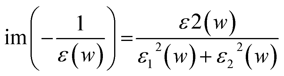
Electronic structure calculations were performed within density functional theory (DFT) framework using the norm-conserving Troullier–Martins pseudopotential as implemented in SIESTA (Spanish Initiative for Electronic Simulations with Thousands of Atoms) program package.54–56 We have used the general gradient approximation (GGA) according to the Perdew–Burke–Ernzerhof (PBE) parameterization for exchange and correlation energies.57,58 Double-zeta basis with polarization (DZP) orbitals are used to expand the Kohn–Sham wavefunctions. Minimization of energy was carried out using the standard conjugate-gradient (CG) technique. The structures were relaxed until the forces on each atom were less than 0.01 eV Å−1. The spacing of real-space grids used to calculate the Hartree and exchange–correlation potentials was taken as 250 Ry. We used supercell geometry with a vacuum of about 20 Å in all directions so that the interactions between two adjacent flakes in the periodic arrangement are negligible.Optical broadening of 0.2 eV was used for dielectric properties calculations. All the unoccupied states have been considered for the calculations of optical spectra. The imaginary part of dielectric function (ε2) has been estimated by calculating the dipolar transition matrix elements between occupied and unoccupied single electron eigenstates.54 The real part of dielectric function (ε1) has been obtained using Kramers–Kroning transformations. Finally, the electron energy loss spectra (EELS) was calculated using ε1 and ε2 in the following formula:
3. Results and discussion
We have considered three different shapes of nanoflakes with two types of edges (Fig. 1). The triangular (T), parallelogram (P) and hexagonal (H) nanoflakes with zigzag (ZZ) edges are modelled with 33, 46 and 54 P-atoms, respectively. Similarly, nanoflakes containing armchair (AC) edges consist of 36, 72 and 114 P atoms, respectively. Next, we considered the edge passivation of both ZZ and AC edges with H-atoms (Fig. S1 of ESI†) to investigate the change in electronic and optical features. The edges are passivated with 15, 18 and 18 H-atoms in ZZ flakes while 18, 26 and 30 H-atoms were considered to passivate AC edge nanoflakes.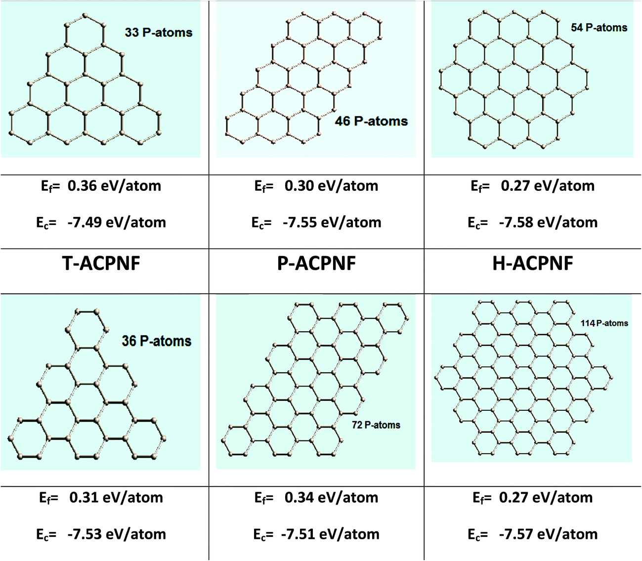 | ||
| Fig. 1 Various β-phosphorene nanoflakes with zigzag (ZZ) and armchair (AC) edge structures with triangular (T), parallelogram (P) and hexagonal (H) shapes. The formation energy (Ef) and cohesive energy (Ec) are also shown with each nanoflakes. | ||
In order to investigate the relative stability of blue phosphorene nanoflakes (BPNFs), we have computed the formation energy and cohesive energy of both zigzag phosphorene nanoflakes (ZZPNFs) and armchair phosphorene nanoflakes (ACPNFs). The formation energy (Ef) per atom is defined as:
| Ef = (EPNF − n1EP − n2EH)/(n1 + n2) |
| Ec = (EPNF − n1E1 − n2E2)/(n1 + n2) |
3.1 Electronic properties
Our spin-polarized calculations for triangular zigzag phosphorene nanoflake (T-ZZPNF) show distinctly different contribution of electronic states for spin up and spin down density of states (DOS) near the Fermi energy, as shown in Fig. 2(a), which indicates the magnetic character of the considered configuration of nanoflake. In general, the magnetic moment for an even number of electrons cancels with each other whereas an odd number of electrons leads to a magnetic character. T-ZZPNF has 15 unpaired electrons at the edges which contribute to the total magnetic moment of 3 μB per structure unit (Table 1). The highest occupied molecular orbital (HOMO)–lowest unoccupied molecular orbital (LUMO) gap for T-ZZPNF is calculated as 0.75 eV for up spin and 0.58 eV for down spin [Fig. 2(a)].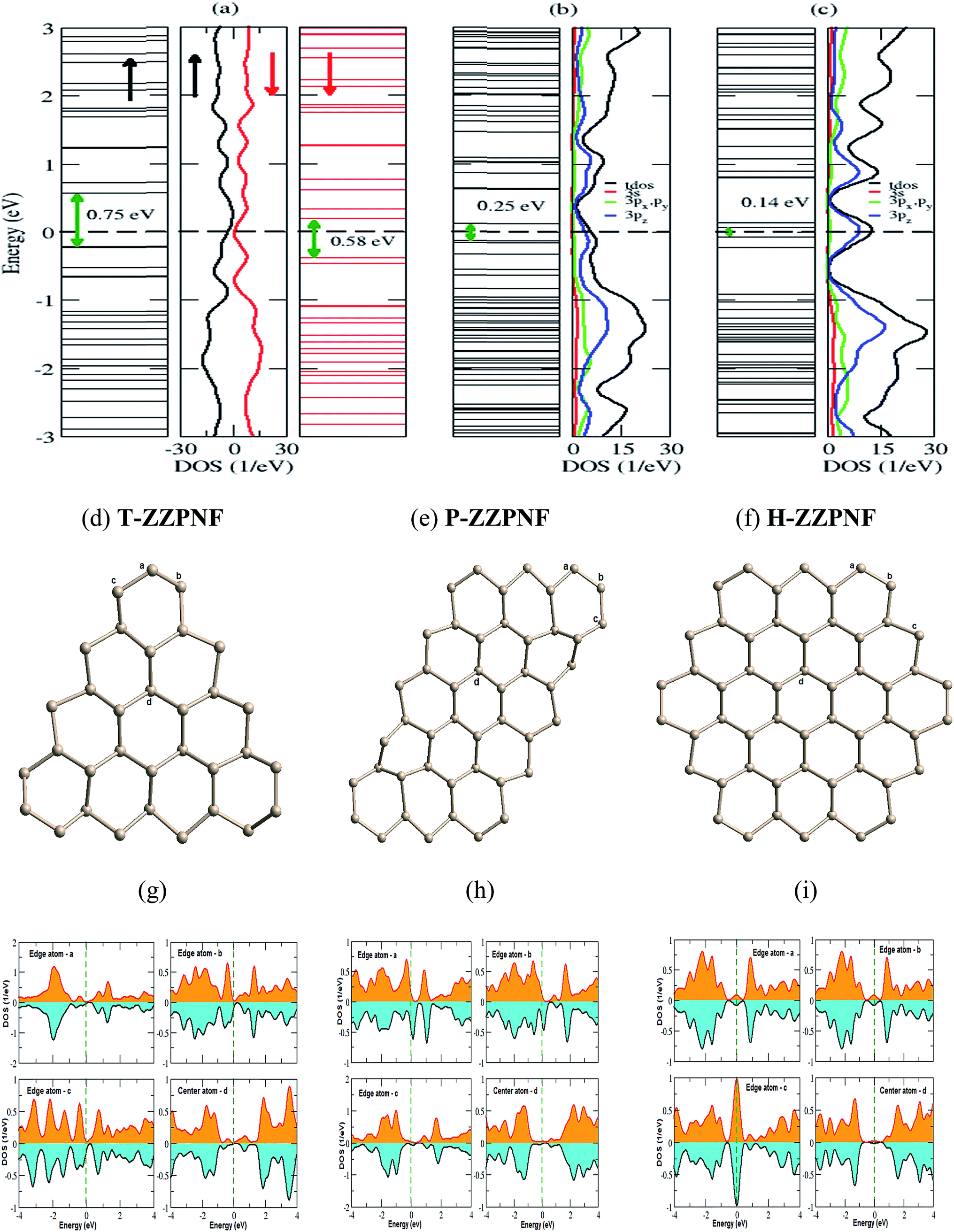 | ||
| Fig. 2 Energy levels and corresponding DOS for (a) T-ZZPNF, (b) P-ZZPNF and (c) H-ZZPNF. The corresponding fully relaxed structures are shown in (d)–(f). The PDOS of edge and center atoms are indicated in the relaxed structures and are given in (g)–(i). | ||
| Nanoflakes | Without passivation | With H-passivation | ||||||
|---|---|---|---|---|---|---|---|---|
| No. atoms | Cavg. | Ravg/Å | θavg/deg | Eg/eV | Magnetic moment/μB | No. atoms | Eg/eV | |
| T-ZZPNF | 33 | 2.38 | 2.18 | 104.07 | 0.75↑, 0.58↓ | 3 | 48 | 2.77 |
| P-ZZPNF | 46 | 2.33 | 2.19 | 104.39 | 0.25 | 0 | 64 | 2.50 |
| H-ZZPNF | 54 | 2.40 | 2.17 | 105.84 | 0.14 | 0 | 72 | 2.56 |
| T-ACPNF | 36 | 2.80 | 2.26 | 94.30 | 1.86↑, 0.97↓ | 6 | 54 | 2.68 |
| P-ACPNF | 72 | 2.57 | 2.24 | 94.24 | 1.85↑, 0.88↓ | 22 | 98 | 2.39 |
| H-ACPNF | 112 | 2.44 | 2.24 | 99.87 | 1.88↑, 0.98↓ | 30 | 142 | 2.31 |
The parallelogram zigzag phosphorene nanoflake (P-ZZPNF) shows a nonmagnetic semiconducting nature with calculated HOMO–LUMO gap of 0.25 eV as shown in Fig. 2(b). The nonmagnetic character is attributed to the even number of electrons (18) present at the edges which cancel out the magnetic character. Similarly, the hexagonal zigzag phosphorene nanoflake (H-ZZPNF) shows a nonmagnetic character with a HOMO–LUMO gap 0.14 eV [Fig. 2(c)]. The nonmagnetic character is also attributed to the even number of electrons (18) at the edges.
In order to quantify the electronic and magnetic behaviour of various ZZPNFs, we have calculated the DOS for bulk and edge atoms of fully relaxed structures [Fig. 2(d)–(f)]. It is clear from the DOS of spin up and spin down states in Fig. 2(g) that the magnetic moment in T-ZZPNF is mainly contributed by the edge atoms. On the other hand, all types of edge atoms show negligible shift in the spin up and spin down DOS of both P-ZZPNF and H-ZZPNF [Fig. 2(h) and (i)] which results into nearly zero magnetic moment in these flakes.
Furthermore, we have analysed the coordination number, bond length and bond angle of edge atoms. Note that the coordination number, P–P bond length and P–P–P bond angle of bulk atoms in ZZPNF are 3, 2.31 Å and 113.54°, respectively. We calculated the average coordination number 2.38 in T-ZZPNF as compared to 3 in bulk atoms. The average P–P bond length of edge atoms of T-ZZPNF reduces to 2.18 Å, while the average P–P–P bond angle of edge atoms decreases to 104.07°. Similarly, a substantial reduction in the above values has been noted for P-ZZPNF and H-ZZPNF (Table 1), that influence the electronic and magnetic behaviour of the considered nanoflakes.
Spin-polarized calculations of armchair β-phosphorene nanoflakes show significant relative displacement of spin up and spin down states in the vicinity of the Fermi energy [Fig. 3(a)–(c)], which indicates the magnetic character of the considered configurations. Interestingly, T-ACPNF shows strong reconstruction of atoms on the corners by forming pentagon structures [Fig. 3(d)]. The c-type edge atoms and the bulk atoms mainly contribute to the 6 μB magnetic moment per structure unit in T-ACPNF [Fig. 3(g)]. The HOMO–LUMO gap has been calculated as 1.86 eV for up spin and 0.97 eV for down spin state.
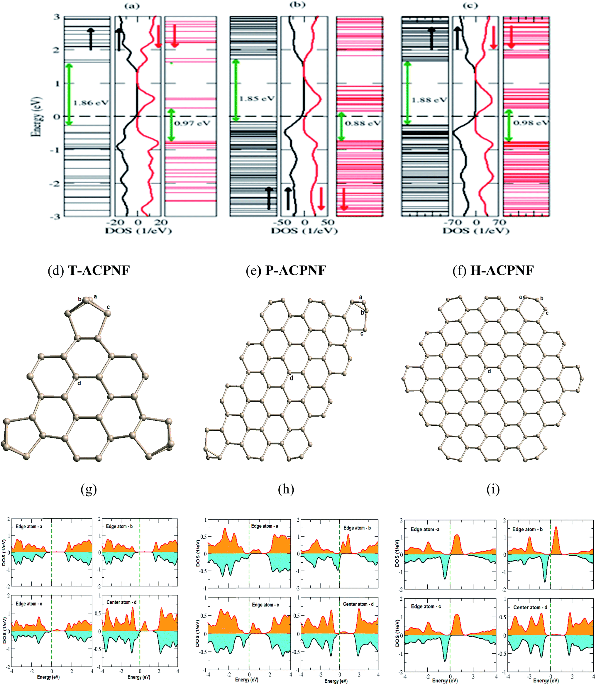 | ||
| Fig. 3 Energy levels and corresponding DOS for (a) T-ACPNF, (b) P-ACPNF and (c) H-ACPNF. The corresponding fully relaxed structures are shown in (d)–(f). The PDOS of edge and center atoms are indicated in the relaxed structures and are given in (g)–(i). | ||
P-ACPNF shows strong magnetic behaviour with 22 μB magnetic moment per structure unit. There are 26 electrons at the edges, 20 are unpaired and 6 are paired with internal P-atoms. The corner atoms of the flake show strong reconstruction as shown in Fig. 3(e). The magnetic moment mainly comes from all types of edge atoms which contribute at the Fermi level. The HOMO–LUMO gap is calculated as 1.85 eV for up spin and 0.88 eV for down spin states. Similarly, H-ACPNF shows a 30 μB magnetic moment per structure unit which is mainly attributed to the unpaired electrons of the edge atoms which can be seen from the DOS contribution of edge atoms around the Fermi level [Fig. 3(i)]. The significant change in the coordination number, bond length and bond angle of edge atoms has been noted in all the armchair edge configurations (Table 1) which influence the electronic and magnetic behaviour of considered nanoflakes. Furthermore, in order to investigate the energetically favourable magnetic order of the magnetic nanoflakes, we calculate the antiferromagnetic (AFM) ground state energy of the flakes and found that there is very small energy difference between FM and AFM states. The difference in ground state energy was calculated as 90, 130, 60 and 5 meV per atom for H-ACPNF, P-ACPNF, T-ACPNF and T-ZZPNF, respectively, that suggest study on AFM and ferromagnetic ordering of given magnetic nanoflakes should be undertaken.
Next we consider the edge passivation of considered nanoflakes with H-atoms. It is found that the unpaired electrons on the edges make bonds with hydrogen atoms that results in an increase in the energy gap. All the considered configurations of β-phosphorene nanoflakes with H-passivation on the edges reveal wide gap semiconductors with HOMO–LUMO gaps ranging from ∼2.3 to ∼2.8 eV (Table 1). It is found that the HOMO–LUMO gap has strong dependence on the edge structure and the shape of nanoflakes (Fig. 4). On analysing the partial density of states (PDOS), we found that 3pz orbitals of P atoms mainly contributed in the vicinity of the Fermi level.
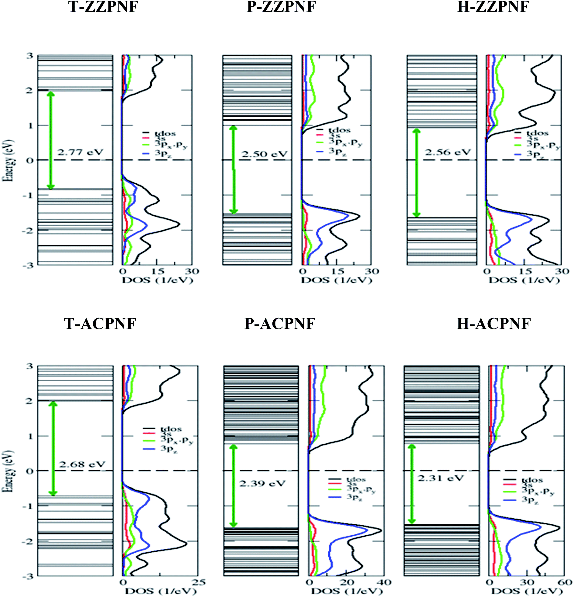 | ||
| Fig. 4 Energy states and corresponding total and partial density of states of H-passivated nanoflakes with various edge and shape structures. | ||
3.2 Dielectric properties
The structure peaks in the imaginary part of dielectric function (ε2) is related with the interband transitions in the corresponding electronic structure. The structure peaks in EELS signifies the collective excitations of electrons at that energy. In general, low energy EELS peaks indicate the collective excitation of weak π electrons, whereas the higher energy EELS peaks are related with both π and σ electron excitations.28 The static dielectric constant (εs) has been investigated by calculating the value of real part of dielectric function (ε1) at zero frequency. The dielectric functions can have two possible orientations of electric vector, namely out-of-plane and in-plane polarization in the considered nanoflakes.The complex dielectric functions and calculated EELS of triangular (T), parallelogram (P) and hexagonal (H) β-phosphorene nanoflakes without passivation for both edge structures are depicted in Fig. 5. Dielectric functions are anisotropic in the low energy range (below 10 eV) and become isotropic in higher energy range (Fig. 5 and S3 of ESI†]. The intensity of ε2 in ACPNF is an order of magnitude higher than the intensity in ZZPNF which is attributed to the higher number of energy levels available for inter-level transitions in ACPNF as compared to ZZPNF (Fig. 4). The broad structure peaks in ε2 for out-of-plane polarization indicate the multiple inter-level transitions, which show a small red shift on going from ZZPNF to ACPNF, that results into the dependence of ε2 on the edge structure of the flakes.
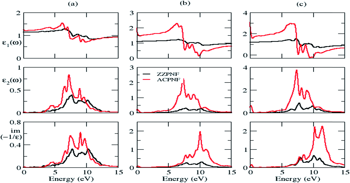 | ||
| Fig. 5 Real part of dielectric function (ε1), imaginary part of dielectric function (ε2), and electron energy loss spectra of unpassivated ZZPNF and ACPNF with (a) triangular (T), (b) parallelogram (P) and (c) hexagonal (H) shape, for out-of-plane polarization. | ||
The static dielectric constant (εs) increases on going from unpassivated ZZ to AC edge structure in both polarization directions (Table 2). The εs of P-ACPNF and H-ACPNF is calculated as 27.3 and 39.9, respectively, for in-plane polarization which indicates the tendency of these flakes to show higher metallicity. The electron energy loss spectra (EELS) for out-of-plane polarization show broad plasmonic structure above 5 eV energy which may be attributed to the collective excitations of both π and σ electrons of flakes (Fig. 5). Note that EELS for in-plane polarization show some structure below 1 eV energy (Fig. S3 of ESI†), however, such small energy plasmonic structures may be due to the interlevel transitions of weakly bound electrons. On carefully looking at the plasmon energy values which have been roughly estimated in Table 2, we found a systematic shift in the plasmonic structure on going across ZZPNF to ACPNF that indicate the edge-dependent EELS. Similarly, systematic blue shift in the energy has been noted as one goes from a triangular (T) to parallelogram (P) to hexagonal (H) nanoflakes for both ZZ and AC edge configurations with both out-of-plane and in-plane polarization, that results in the shape-dependent EELS.
| Nanoflakes | Without passivation | With H-passivation | ||||||
|---|---|---|---|---|---|---|---|---|
| εs | Plasmon energy/eV | εs | Plasmon energy/eV | |||||
| Out-of-plane | In-plane | Out-of-plane | In-plane | Out-of-plane | In-plane | Out-of-plane | In-plane | |
| T-ZZPNF | 1.1 | 2.3 | 7.8 | 5.1 | 1.2 | 1.2 | 9.3 | 9.1 |
| P-ZZPNF | 1.2 | 3.4 | 9.8 | 5.3 | 1.1 | 1.1 | 9.4 | 5.4 |
| H-ZZPNF | 2.0 | 6.4 | 10.1 | 5.4 | 1.2 | 1.4 | 9.3 | 5.2 |
| T-ACPNF | 1.3 | 3.7 | 9.1 | 7.4 | 1.3 | 1.4 | 9.8 | 9.2 |
| P-ACPNF | 1.9 | 27.3 | 10.0 | 9.8 | 1.5 | 1.8 | 10.0 | 9.7 |
| H-ACPNF | 3.1 | 39.9 | 11.4 | 10.1 | 1.6 | 2.1 | 10.3 | 9.6 |
Next we investigated the dielectric functions and EELS of hydrogen-passivated edges of various nanoflakes configurations (Fig. 6 and S4 of ESI†). The ε2 of AC edge structures has higher intensity than ZZ edge flakes which is attributed to the higher number of available atomic levels for interband transitions. The static dielectric constant has been calculated to be in the range of 1.2 to 2.1 (Table 1). As we go from ZZ edge configurations to AC edge configurations, the static dielectric constant (εs) shows an increase in its magnitude which is inverse of the HOMO–LUMO gap (Eg) calculated in Table 1. This can be understand within the framework of the Penn model expression:59
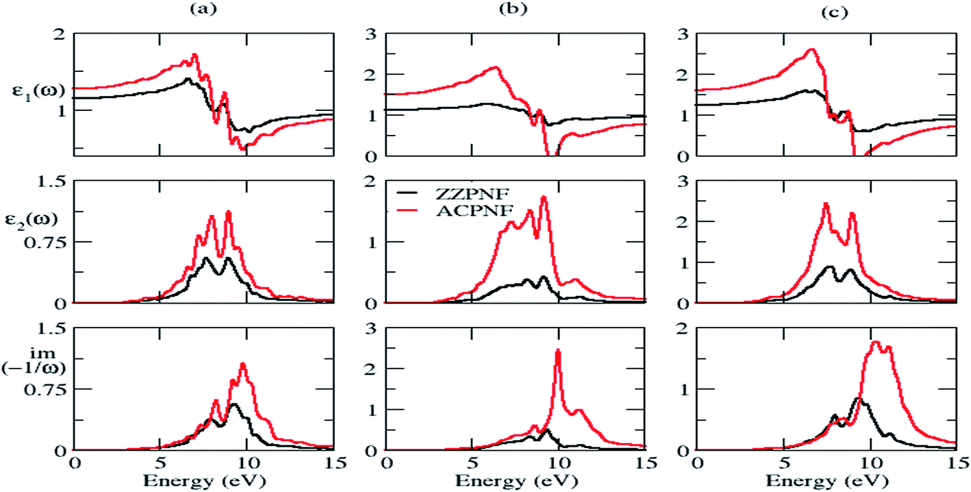 | ||
| Fig. 6 Real part of dielectric function (ε1), imaginary part of dielectric function (ε2) and electron energy loss spectra of hydrogen passivated ZZPNF and ACPNF with (a) triangular (T), (b) parallelogram (P) and (c) hexagonal (H) shape, for out-of-plane polarization. | ||
It is noticeable that the considered nanoflakes have shape- and size-dependent dielectric properties. Particularly, the EELS show strong sensitivity to the edge configurations and shape structures. For example, T-ZZPNF and P-ZZPNF without passivation has ∼2 eV energy difference in EELS for out-of-plane polarization and the same flakes with edge passivation show ∼3.5 eV energy difference for in-plane polarization. Similarly, we found significantly large plasmonic energy difference for a nanoflake with a particular shape having different edge configurations. Therefore, electron energy loss spectroscopy may be useful to determine the various shapes and edge configurations of the considered nanoflakes.
3.3 Size effect on electronic and dielectric properties
Next we consider the effect of size on electronic and dielectric properties of nanoflakes. As a representative case, parallelogram-shaped PNF has been taken for study. It is found that the size of PNF has significant impact on the electronic structure (Fig. S5 of ESI†), e.g. the energy gap of bare ZZPNF shows more than 50% decrease in magnitude on increasing the size from P28 to P46; the spin up energy gap of ACPNF decreases while spin down gap shows a marginal increase on increasing the size from P36 to P72; hydrogen passivated nanoflakes also show a size effect with decrease in energy gap with increasing number of atoms in the nanoflakes. The size effect on the dielectric properties has also been shown by nanoflakes which is more pronounced for ACPNF (Fig. 7), e.g. the static dielectric constant of ACPNF increases from 1.4 to 1.9 on increasing the size; EELS shows a blue shift in plasmonic energy from 9.6 to 10.1 eV. The variable energy gap and tunable dielectric properties of PNFs which depends on the edge configurations, shape and size of flakes makes the studied nanostructures potentially useful for optoelectronic applications.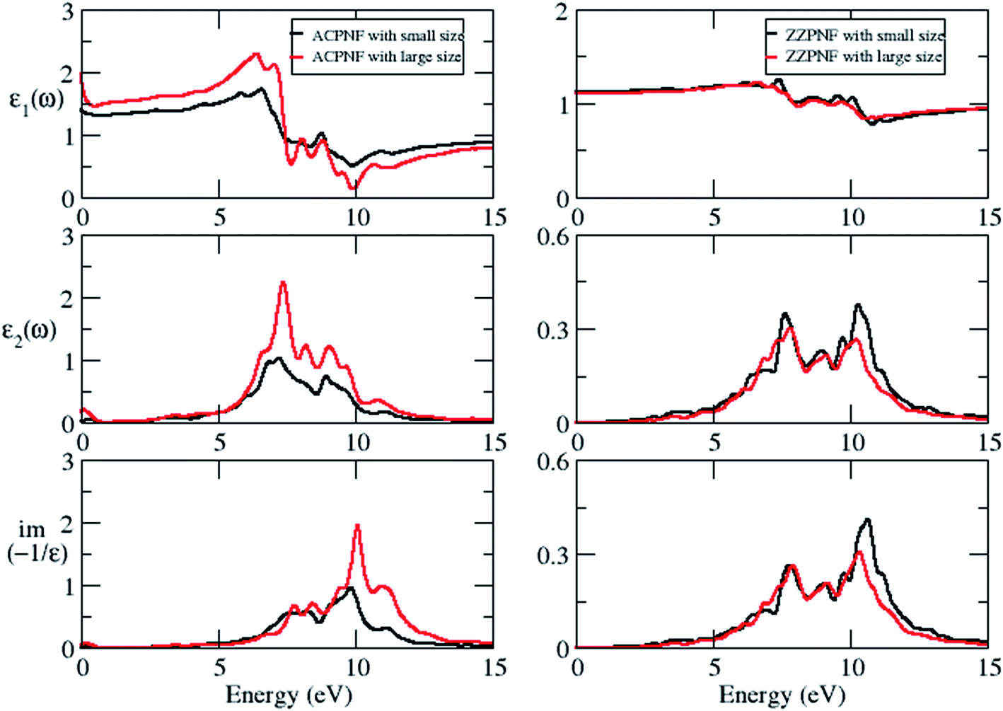 | ||
| Fig. 7 Real part of dielectric function (ε1), imaginary part of dielectric constant (ε2), electron energy loss spectra of parallelogram (P) shape ZZPNF and ACPNF with size effect, for out-of-plane polarization. Small size ACPNF and ZZPNF have 36 and 28 atoms, respectively, while large size flakes have 72 and 46 atoms, respectively. | ||
4. Summary
In summary, we have performed a detailed first principles study of the electronic and dielectric properties of β-phosphorene nanoflakes. It is found that the energy gap of unpassivated β-phosphorene nanoflakes with AC edges is larger than for ZZ edges. The unpassivated AC edge structures are magnetic semiconductors while hydrogen passivated structures show increased HOMO–LUMO gap with non-magnetic character. The magnetic nature of unpassivated AC edge configurations is attributed to the dangling bond states and the magnitude of magnetic moment depends upon the reconstruction of edge atoms. Dielectric functions are highly anisotropic in the low energy range and show isotropic behaviour at higher energy. The intensity of the imaginary part of the dielectric function for AC edge structures show higher intensity than ZZ edge configurations due to the higher number of available states for interband transitions in AC nanoflakes. The static dielectric constant shows strong dependence on the types of shape and edge structure of considered nanoflakes. The electron energy loss spectra show distinctly different plasmonic features for considered nanoflakes. The tunable electronic and dielectric properties of the considered nanoflakes may find applications in optoelectronic devices based on β-phosphorene.Acknowledgements
PB and RS are grateful to the Central University of Punjab for financial assistance. We acknowledge the computational facilities at CUPB for current research work.References
- S. Zhao, W. Kang and J. Xue, The potential application of phosphorene as an anode material in Li-ion batteries, J. Mater. Chem. A, 2014, 2(44), 19046–19052 CAS.
- P. Yasaei, A. Behranginia, T. Foroozan, M. Asadi, K. Kim, F. Khalili-Araghi and A. Salehi-Khojin, Stable and Selective Humidity Sensing Using Stacked Black Phosphorus Flakes, ACS Nano, 2015, 9(10), 9898–9905 CrossRef CAS PubMed.
- V. V. Kulish, O. I. Malyi, C. Persson and P. Wu, Phosphorene as an anode material for Na-ion batteries: a first-principles study, Phys. Chem. Chem. Phys., 2015, 17(21), 13921–13928 RSC.
- A. D. Franklin, Nanomaterials in transistors: From high-performance to thin-film applications, Science, 2015, 349(6249), aab2750 CrossRef PubMed.
- H. Du, X. Lin, Z. Xu and D. Chu, Recent developments in black phosphorus transistors, J. Mater. Chem. C, 2015, 3(34), 8760–8775 RSC.
- K. S. Novoselov, A. K. Geim, S. V. Morozov, D. Jiang, Y. Zhang, S. V. Dubonos, I. V. Grigorieva and A. A. Firsov, Electric field effect in atomically thin carbon films, Science, 2004, 306(5696), 666–669 CrossRef CAS PubMed.
- J. C. Meyer, A. K. Geim, M. I. Katsnelson, K. S. Novoselov, T. J. Booth and S. Roth, The structure of suspended graphene sheets, Nature, 2007, 446(7131), 60–63 CrossRef CAS PubMed.
- A. K. Geim and K. S. Novoselov, The rise of graphene, Nat. Mater., 2007, 6(3), 183–191 CrossRef CAS PubMed.
- S. Z. Butler, S. M. Hollen, L. Cao, Y. Cui, J. A. Gupta, H. R. Gutierrez, T. F. Heinz, S. S. Hong, J. Huang and A. F. Ismach, et al., Progress, challenges, and opportunities in two-dimensional materials beyond graphene, ACS Nano, 2013, 7(4), 2898–2926 CrossRef CAS PubMed.
- A. Kara, H. Enriquez, A. P. Seitsonen, L. C. L. Y. Voon, S. Vizzini, B. Aufray and H. Oughaddou, A review on silicene—new candidate for electronics, Surf. Sci. Rep., 2012, 67(1), 1–18 CrossRef CAS.
- Y. Yamada-Takamura and R. Friedlein, Progress in the materials science of silicene, Sci. Technol. Adv. Mater., 2016, 15(6), 1–12 Search PubMed.
- M. Houssa, E. Scalise, K. Sankaran, G. Pourtois, V. V. Afanas’ev and A. Stesmans, Electronic properties of hydrogenated silicene and germanene, Appl. Phys. Lett., 2011, 98(22), 223107 CrossRef.
- D. Jariwala, V. K. Sangwan, L. J. Lauhon, T. J. Marks and M. C. Hersam, Emerging device applications for semiconducting two-dimensional transition metal dichalcogenides, ACS Nano, 2014, 8(2), 1102–1120 CrossRef CAS PubMed.
- A. Kumar and P. K. Ahluwalia, Electronic transport and dielectric properties of low-dimensional structures of layered transition metal dichalcogenides, J. Alloys Compd., 2014, 587, 459–467 CrossRef CAS.
- B. Radisavljevic, A. Radenovic, J. Brivio, V. Giacometti and A. Kis, Single-layer MoS2 transistors, Nat. Nanotechnol., 2011, 6(3), 147–150 CrossRef CAS PubMed.
- S. Bagheri, N. Mansouri and E. Aghaie, Phosphorene: a new competitor for graphene, Int. J. Hydrogen Energy, 2016, 41(7), 4085–4095 CrossRef CAS.
- L. Kou, C. Chen and S. C. Smith, Phosphorene: fabrication, properties, and applications, J. Phys. Chem. Lett., 2015, 6(14), 2794–2805 CrossRef CAS PubMed.
- L. Li, Y. Yu, G. J. Ye, Q. Ge, X. Ou, H. Wu, D. Feng, X. H. Chen and Y. Zhang, Black phosphorus field-effect transistors, Nat. Nanotechnol., 2014, 9(5), 372–377 CrossRef CAS PubMed.
- W. L. Wang, S. Meng and E. Kaxiras, Graphene nanoflakes with large spin, Nano Lett., 2008, 8(1), 241–245 CrossRef CAS PubMed.
- H. Liu, A. T. Neal, Z. Zhu, Z. Luo, X. Xu, D. Tomanek and P. D. Ye, Phosphorene: an unexplored 2D semiconductor with a high hole mobility, ACS Nano, 2014, 8(4), 4033–4041 CrossRef CAS PubMed.
- J. Kang, S. A. Wells, J. D. Wood, J. Lee, X. Liu, C. R. Ryder, J. Zhu, J. R. Guest, C. A. Husko and M. C. Hersam, Stable aqueous dispersions of optically and electronically active phosphorene, Proc. Natl. Acad. Sci. U. S. A., 2016, 201602215 Search PubMed.
- A. Castellanos-Gomez, L. Vicarelli, E. Prada, J. O. Island, K. L. Narasimha-Acharya, S. I. Blanter, D. J. Groenendijk and M. Buscema, et al., Isolation and characterization of few-layer black phosphorus, 2D Materials, 2014, 1(2), 025001 CrossRef.
- D. Warschauer, Electrical and optical properties of crystalline black phosphorus, J. Appl. Phys., 1963, 34(7), 1853–1860 CrossRef CAS.
- A. Brown and S. Rundqvist, Refinement of the crystal structure of black phosphorus, Acta Crystallogr., 1965, 19(4), 684–685 CrossRef CAS.
- J. Qiao, X. Kong, Z. Hu, F. Yang and W. Ji, High-mobility transport anisotropy and linear dichroism in few-layer black phosphorus, Nat. Commun., 2014, 5, 1–7 Search PubMed.
- Z. Zhu and D. Tomanek, Semiconducting layered blue phosphorus: A computational study, Phys. Rev. Lett., 2014, 112(17), 176802 CrossRef PubMed.
- Y. Cai, G. Zhang and Y. Zhang, Layer-dependent band alignment and work function of few-layer phosphorene, Sci. Rep., 2014, 4, 1–19 Search PubMed.
- W. L. Wang, O. V. Yazyev, S. Meng and E. Kaxiras, Topological frustration in graphene nanoflakes: magnetic order and spin logic devices, Phys. Rev. Lett., 2009, 102(15), 157201 CrossRef PubMed.
- A. H. Reshak, S. A. Khan and S. Auluck, Thermoelectric properties of a single graphene sheet and its derivatives, J. Mater. Chem. C, 2014, 2(13), 2346–2352 RSC.
- A. Kumar and P. K. Ahluwalia, Tunable electronic and dielectric properties of molybdenum disulfide in MoS2: materials physics and devices, Springer, 2014, pp. 1–35 Search PubMed.
- J. Li, Z. H. Zhang, D. Wang, Z. Zhu, Z. Q. Fan, G. P. Tang and X. Q. Deng, Electronic structures, field effect transistor and bipolar field-effect spin filtering behaviors of functionalized hexagonal graphene nanoflakes, Carbon, 2014, 69, 142–150 CrossRef CAS.
- A. S. Barnard and I. K. Snook, Modelling the role of size, edge structure and terminations on the electronic properties of graphene nano-flakes, Modell. Simul. Mater. Sci. Eng., 2011, 19(5), 054001 CrossRef.
- Y. Son, M. L. Cohen and S. G. Louie, Half-metallic graphene nanoribbons, Nature, 2006, 444(7117), 347–349 CrossRef CAS PubMed.
- W. Li, G. Zhang and Y. Zhang, Electronic properties of edge-hydrogenated phosphorene nanoribbons: a first-principles study, J. Phys. Chem. C, 2014, 118(38), 22368–22372 CAS.
- W. Hu, L. Lin, C. Yang, J. Dai and J. Yang, Edge-Modified Phosphorene Nanoflake Heterojunctions as Highly Efficient Solar Cells, Nano Lett., 2016, 16(3), 1675–1682 CrossRef CAS PubMed.
- Y. Jing, X. Zhang, and Z. Zhou, Phosphorene: what can we know from computations?, Wiley Interdisciplinary Reviews: Computational Molecular Science, 2016, vol. 6, 1, pp. 5–19 Search PubMed.
- J.-O. Joswig, T. Lorenz, T. B. Wendumu, S. Gemming and G. Seifert, Optics, mechanics, and energetics of two-dimensional MoS2 nanostructures from a theoretical perspective, Acc. Chem. Res., 2014, 48(1), 48–55 CrossRef PubMed.
- M. De Corato, C. Cocchi, D. Prezzi, M. J. Caldas, E. Molinari and A. Ruini, Optical Properties of Bilayer Graphene Nanoflakes, J. Phys. Chem. C, 2014, 118(40), 23219–23225 CAS.
- K. A. Ritter and J. W. Lyding, The influence of edge structure on the electronic properties of graphene quantum dots and nanoribbons, Nat. Mater., 2009, 8(3), 235–242 CrossRef CAS PubMed.
- X. Peng, A. Copple and Q. Wei, Edge effects on the electronic properties of phosphorene nanoribbons, J. Appl. Phys., 2014, 116(14), 144301 CrossRef.
- Y. Cai, G. Zhang and Y.-W. Zhang, Polarity-reversed robust carrier in monolayer MoS2 nanoribbons, J. Am. Chem. Soc., 2014, 136(17), 6269 CrossRef CAS PubMed.
- Y. Cai, Q. Ke, G. Zhang, Y. P. Feng, V. B. Shenoy and Y.-W. Zhang, Giant Phononic Anisotropy and Unusual Anharmonicity of Phosphorene: Interlayer Coupling and Strain Engineering, Adv. Funct. Mater., 2015, 25, 2230 CrossRef CAS.
- Y. Cai, Q. Ke, G. Zhang and Y.-W. Zhang, Energetics, Charge Transfer, and Magnetism of Small Molecules Physisorbed on Phosphorene, J. Phys. Chem. C, 2015, 119(6), 3102 CAS.
- Y. Cai, G. Zhang and Y.-W. Zhang, Electronic Properties of Phosphorene/Graphene and Phosphorene/Hexagonal Boron Nitride Heterostructures, J. Phys. Chem. C, 2015, 119(24), 13929 CAS.
- Y. Wang and N. Herron, Nanometer-sized semiconductor clusters: materials synthesis, quantum size effects, and photophysical properties, J. Phys. Chem., 1991, 95(2), 525–532 CrossRef CAS.
- Q. Wu, L. Shen, M. Yang, Y. Cai, Z. Huang and Y. P. Feng, Electronic and transport properties of phosphorene nanoribbons, Phys. Rev. B: Condens. Matter Mater. Phys., 2015, 92(3), 035436 CrossRef.
- J. Dai and X. C. Zeng, Bilayer phosphorene: effect of stacking order on bandgap and its potential applications in thin-film solar cells, J. Phys. Chem. Lett., 2014, 5(7), 1289–1293 CrossRef CAS PubMed.
- M. Bernardi, M. Palummo and J. C. Grossman, Semiconducting monolayer materials as a tunable platform for excitonic solar cells, ACS Nano, 2012, 6(11), 10082–10089 CrossRef CAS PubMed.
- L.-J. Zhou, Y.-F. Zhang and L.-M. Wu, SiC2 siligraphene and nanotubes: novel donor materials in excitonic solar cells, Nano Lett., 2013, 13(11), 5431–5436 CrossRef CAS PubMed.
- J. Gao, G. Zhang and Y.-W. Zhang, The Critical Role of Substrate in Stabilizing Phosphorene Nanoflake: A Theoretical Exploration, J. Am. Chem. Soc., 2016, 138(14), 4763–4771 CrossRef CAS PubMed.
- C. S. Cucinotta, K. Dolui, H. Pettersson, Q. M. Ramasse, E. Long, S. E. O’Brian, V. Nicolosi and S. Sanvito, Electronic Properties and Chemical Reactivity of TiS2 Nanoflakes, J. Phys. Chem. C, 2015, 119(27), 15707–15715 CAS.
- C. K. Gan and D. J. Srolovitz, First-principles study of graphene edge properties and flake shapes, Phys. Rev. B: Condens. Matter Mater. Phys., 2010, 81(12), 125445 CrossRef.
- H.-X. Luan, C.-W. Zhang, F. Li and P.-J. Wang, Electronic and magnetic properties of silicene nanoflakes by first-principles calculations, Phys. Lett. A, 2013, 377(39), 2792–2795 CrossRef CAS.
- J. M. Soler, E. Artacho, J. D. Gale, A. G. J. Junquera, P. Ordejon and D. Sanchez-Portalet, The SIESTA method for ab initio order-N materials simulation, J. Phys.: Condens. Matter, 2002, 14(11), 2745 CrossRef CAS.
- W. Kohn, A. D. Becke and R. G. Parr, Density functional theory of electronic structure, J. Phys. Chem., 1996, 100(31), 12974–12980 CrossRef CAS.
- W. Kohn, Nobel Lecture: Electronic structure of matter—wave functions and density functionals, Rev. Mod. Phys., 1999, 71(5), 1253 CrossRef CAS.
- J. P. Perdew, K. Burke and Y. Wang, Erratum: Generalized gradient approximation for the exchange–correlation hole of a many-electron system [Phys. Rev. B 54, 16 533 (1996)], Phys. Rev. B: Condens. Matter Mater. Phys., 1998, 57(23), 14999 CrossRef CAS.
- J. P. Perdew, K. Burke and Y. Wang, Generalized gradient approximation for the exchange–correlation hole of a many-electron system, Phys. Rev. B: Condens. Matter Mater. Phys., 1996, 54(23), 16533 CrossRef CAS.
- D. R. Penn, Wavenumber-dependent-dielectric function of demiconductors, Phys. Rev., 1962, 128, 2093 CrossRef CAS.
Footnote |
| † Electronic supplementary information (ESI) available. See DOI: 10.1039/c6ra16534f |
| This journal is © The Royal Society of Chemistry 2016 |