Yan-Jie Liu†
a,
Hong-Di Zhang†*a,
Xu Yanab,
Ai-Jing Zhaoa,
Zhi-Guang Zhanga,
Wen-Yan Sia,
Mao-Gang Gonga,
Jun-Cheng Zhanga and
Yun-Ze Long*ab
aCollaborative Innovation Center for Nanomaterials & Optoelectronic Devices, College of Physics, Qingdao University, Qingdao 266071, China. E-mail: hongdi_zhang@163.com; yunze.long@163.com
bIndustrial Research Institute of Nonwovens & Technical Textiles, College of Textiles & Clothing, Qingdao University, Qingdao 266071, China
First published on 29th August 2016
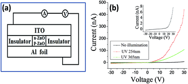
Pure n-type ZnO nanofibers and p-type Ce-doped ZnO nanofibers were prepared by electrospinning followed by calcination. Their surface morphology, elemental composition, crystal structure, and optical and electronic properties were characterized by scanning electron microscopy, energy-dispersive X-ray spectroscopy, X-ray diffraction, and photoluminescence and UV-visible spectroscopy techniques and by their current–voltage (I–V) curves. The energy-dispersive X-ray spectroscopy and X-ray diffraction spectra showed that Ce was successfully incorporated into the ZnO crystal lattice and that the atomic percentage of Ce to Zn was 1.46%. The photoluminescence integrated intensity ratio of the UV emission to the deep-level green emission for Ce-doped ZnO nanofibers was over twice than that of pure ZnO. The UV-visible absorption edge of the Ce-doped ZnO nanofibers red-shifted by 2.6 nm compared with the pure ZnO nanofibers. The ZnO nanofibers had a good response to ultraviolet radiation. The sensitivity (Imax/I0) of the Ce-doped ZnO nanofibers was 102, which was one order higher in magnitude than that of pure ZnO nanofibers. The field-effect curve suggested that the synthesized Ce-doped ZnO nanofibers were p-type semiconductors. A p–n homojunction device was prepared using the ZnO nanofibers and showed good rectifying behavior. The turn-on voltage reduced by about 10 V under UV irradiation. Both the ZnO nanofibers and the ZnO p–n homojunction had excellent UV sensibilities. These results suggest that Ce-doped ZnO nanofibers may have widespread applications in optical and electronic devices.
Pure ZnO is an n-type semiconductor as a result of its intrinsic defects.6 New techniques to produce high-quality p-type ZnO thin films will facilitate their application. However, it is difficult to prepare p-type ZnO by doping, mainly due to the low solubility of the acceptor dopants, the deep acceptor level and the self-compensation effect of the intrinsic defects.7 Several approaches have been used to prepare p-type ZnO using groups I and V elements as alternative dopants for Zn and O, respectively,8 but the p-type conduction was unstable.9 p-Type ZnO has also been prepared by introducing different dopants via pulsed laser deposition,10 sputtering,11 metal–organic chemical vapor deposition12 and spray pyrolysis techniques.13 Chang et al.14 prepared Ce-doped ZnO nanorods at 90 °C by a hydrothermal method and tested their visible light emission. However, these approaches can only fabricate ZnO membranes and short nanowires so their applications to different devices is limited.15,16 Electrospinning is a good technique for the preparation of ZnO fibers and is simple, versatile and cheap. It can produce both ultrathin and long continuous fibers. García-Méndez et al.17 reported the preparation of Ce-doped ZnO thin films with excellent optical properties by RF-reactive magnetron sputtering technology. p-Type ZnO is difficult to prepare by electrospinning, although ZnO nanofibers have been produced by this technique.18 Lang et al.19 reported the synthesis of Ce-doped ZnO nanorods under mild hydrothermal conditions. The preparation of p-type Ce-doped ZnO fibers and rectifying devices via electrospinning–calcination technology has been reported by our group, but there have only been a few reports of the optoelectronic properties of Ce-doped ZnO nanofibers and ZnO p–n junctions. p–n junctions have wide applications in optical devices such as semiconductor laser diodes and UV photodetectors.20 There has been no previous report of the photosensitivity of pure ZnO/Ce-doped ZnO homojunctions prepared by electrospinning.
We synthesized n-type pure ZnO nanofibers and p-type Ce-doped nanofibers via electrospinning and calcination. ZnO nanofibrous homojunctions were prepared by the same technique. The surface topography, crystal structure, electrical and optical properties and the basic theory of p-type ZnO formation are reported here.
The ZnO p–n homojunction nanofibers were fabricated as follows. The pure ZnO precursor solution was electrospun on the Si wafer. The Ce–ZnO precursor solution was then electrospun as the second fiber membrane under the same conditions of 20 °C, 50% RH, an electrospinning voltage of 20 kV and an electrospinning distance of 13.5 cm. The p–n homojunction nanofibers were formed after the fibrous membrane was calcined in a muffle furnace at 900 °C for 2 h.
The ZnO p–n homojunction device was prepared as follows. The p-type side (lower side) of the ZnO homojunction was connected to aluminum foil and the n-type side (upper side) of the ZnO homojunction was connected to the ITO electrode. The upper and lower sides were then connected to the negative and positive electrodes, respectively, of the power supply using copper conductors.
Fig. 4a shows the elemental analyses of pure ZnO nanofibers analyzed by EDS. The EDS spectrum of pure ZnO nanofibers only contains Zn and O, which demonstrates that the resultant nanofibers are pure ZnO. The EDS result for Ce-doped ZnO nanofibers (Fig. 4b) shows that Ce is also present in the nanofibers. No other peak associated with impurities was observed, indicating that the fabricated nanofibers were Ce-doped ZnO nanofibers. The experimental atomic percentage of Ce to Zn (obtained from the EDS analysis) was 1.46%, which is consistent with the theoretical value. The theoretical value was calculated by the molar ratio of Ce to Zn (0.02 g Ce(NO3)3·6H2O and 1.2 g Zn(CH3COO)2·2H2O). The mass percentage of Ce that can be incorporated into the ZnO host was therefore about 0.891%.
Fig. 5 shows the XRD patterns of the pure ZnO nanofibers and Ce-doped ZnO nanofibers, demonstrating the crystallographic characteristics of the pure ZnO and Ce-doped ZnO nanofibers. The peaks of the diffraction pattern were high and the full-width half-maximum was narrow, which indicated that the pure ZnO and Ce-doped ZnO both had good crystallinity. The XRD spectrum proved that the pure ZnO nanofibers had a hexagonal wurtzite structure (JCPDS 36-1451) with the diffraction peaks at 2θ values of 31.77, 34.42 and 36.26° corresponding to the (100), (002) and (101) lattice planes, respectively. In contrast with the undoped ZnO, a new peak located at 2θ = 28.55°, corresponding to the (111) diffraction peak of CeO2 (JCPDS 34-0394), appears in Ce-doped ZnO nanofibers as a result of doping with Ce ions. Comparison of the XRD profiles for the pure ZnO nanofibers and the Ce-doped ZnO nanofibers showed that the diffraction peaks of the Ce-doped ZnO fibers had a small shift of about 0.31° to a lower angle. The atomic radius of Ce4+ (87 pm) is larger than that of Zn2+ (74 pm), leading to a larger ZnO lattice. According to the Bragg equation, the lattice constant is in proportion to d (the interplanar distance) and the diffraction peaks will shift to smaller angle with increasing atom radius, indicating the incorporation of Ce ions into the ZnO lattice. The XRD results also demonstrated that the synthesized nanofibers were a compound phase with a hexagonal wurtzite structure for ZnO and a cubic structure for CeO2. There was no impurity peak in the XRD patterns, so the samples were of high purity.
![]() | ||
Fig. 5 XRD patterns of pure ZnO and Ce-doped ZnO nanofibers after calcination; inset shows an enlarged view of the (101) diffraction. |
The broad green emission band with a peak near 500 nm is attributed to electron–hole recombination process, in which electron can transfer from the shallow donor level from the intrinsic defect centers, such as interstitial zinc (Zni) and oxygen vacancy (VO), to the valence band6 or conduction band.23 The presence of impurities or excess oxygen24 may also be responsible for the green emission. A weak peak is also observed at about 471 nm, which may be a result of the existence of defects or impurities linked to local levels in the ZnO gap.17 García-Méndez et al.17 reported that the peak of RF-sputtered Ce-doped ZnO membranes appeared at 467 nm because the electric dipole allowed the transition of the Ce3+ ions. These peaks originated from the lower 5d (2D) excited state to the split 2F5/2 and 2F7/2 energy levels.17
When elemental Ce is doped into ZnO nanofibers, the PL intensity of ZnO decreases. The difference in the emission intensity may be associated with their different nanostructural morphology and crystallinity. The doping of Ce may increase lattice defects and lead to a change in the crystal field and band gap, thus decreasing the PL intensity of Ce-doped ZnO nanofibers (Fig. 6a–c). With Ce4+ ions as donors in the ZnO matrix, a small red shift may appear in the UV emission because of a slight modulation of the ZnO band gap and the formation of new emission centers.19 In this case, the luminescent process is changed. Li et al.25 reported that the incorporation of Ce4+ ions resulted in transitions between the 5d and 4f orbits, which may bring about multi-emission peaks in the blue-green region. It is generally considered that the intensity ratio between the UV emission band and the visible emission band is an indicator of ZnO crystalline materials. The intense UV and weak green band correspond to a good crystal surface.26 In this investigation, the PL ratios of the integrated intensity between the UV emission and the deep-level green emission (IUV/IDLE) were 0.2553, 0.3667 and 0.6067 on excitation at 325, 350 and 365 nm for ZnO and 0.5968, 0.7762 and 1.2851 on excitation at 325, 350 and 365 nm for the Ce-doped ZnO nanofibers, respectively. A larger ratio indicates that the Ce-doped ZnO nanofibers have good crystallinity. These results show that Ce-doped ZnO nanofibers have promising applications in optoelectronic devices. The PL intensity is larger at shorter wavelengths because more electrons are excited with increasing energy. IUV/IDLE is larger at longer wavelengths of excitation.
As the energy of UV light is close to the band gap of semiconductors, it is absorbed by many metal oxide semiconductors. Bulk ZnO has a direct band gap of 3.37 eV.16 The optical absorption patterns of the synthesized pure ZnO and Ce-doped ZnO nanofibers were investigated by UV-visible spectrometry (Fig. 7). Fig. 7a shows the absorption of ZnO at different wavelengths. The intersection of the absorbance and photon energy (hν) axes corresponds to the band gap of ZnO nanofibers (Fig. 7b). The synthesized Ce–ZnO nanofibers had a higher absorption coefficient than pure ZnO nanofibers in the UV region (250–400 nm). The absorption edge revealed that the ZnO nanofibers had a direct band gap that could be obtained by extending the linear portion of the absorption pattern to the photon energy of the horizontal axis. For pure ZnO, the point of intersection was 3.10 eV, corresponding to an absorption edge of 398 nm, which was smaller than the cited value of 3.37 eV corresponding to the band-to-band transition of bulk ZnO.27 By contrast, the band gap of Ce–ZnO was about 3.08 eV (at a wavelength of 402 nm). The absorption results revealed that the peak of Ce-doped ZnO nanofibers shifted to longer wavelengths, which can be attributed to quantum confinement and small size effects.28 The ZnO nanofibers effectively absorbed the photon energy when exposed to 254 nm irradiation, which has an energy of 4.9 eV. This is enough energy to excite electrons diametrically from the valence band to the conduction band. The absorption ability may be different in the same material under different irradiation conditions. According to previous research,29 the absorption coefficient of ZnO nanofibers decreases with increasing UV wavelength. Thus the sensitivity of ZnO nanofibers under 365 nm UV irradiation, which has an energy of 3.40 eV, is lower than under 254 nm irradiation. The reduced band gap indicated that the optical properties of Ce-doped ZnO nanofibers was improved.
![]() | ||
Fig. 7 (a) UV-visible absorption spectra of the pure ZnO and Ce-doped ZnO nanofibers and (b) plot of absorbance versus photon energy for ZnO nanofibers. |
Fig. 8a and b show the photoresponse and I–V characteristic curves of pure ZnO and Ce-doped ZnO nanofibers under no illumination and under 254 and 365 nm UV irradiation, respectively. The photocurrents of the pure ZnO nanofibers increased from the background current (under a bias of 30.0 V) of I0 = 6.31 nA to Imax = 2.43 μA (254 nm UV irradiation) and 1.55 μA (365 nm UV irradiation). The photocurrents of Ce-doped ZnO nanofibers increased from a background current of I0 = 1.69 nA to Imax = 1.21 μA (254 nm UV irradiation) and 0.365 μA (365 nm UV irradiation). It is evident from Fig. 8a and b that the photocurrent decreased with increasing UV wavelength. Under UV irradiation of 254 and 365 nm, the photocurrent of the Ce–ZnO nanofibers decreased compared with that of the pure ZnO nanofibers because pure ZnO is intrinsically an n-type semiconductor and is difficult to turn into a p-type semiconductor. The Ce acts as a doping impurity, which reduces the electron concentration and increases the hole concentration in the ZnO nanofibers. Doping of Ce may also increase the lattice defects and decrease the photocurrent (I0 and Imax).
Compared with the initial current I0 (background current), the photocurrent increased enormously. The linear behavior of the I–V characteristics of the ZnO membranes suggests ohmic contacts. When the ZnO nanofibers were periodically exposed to UV irradiation, the current curves changed (Fig. 8c and d). The photocurrent increased and decreased periodically when the UV lamp was switched on and off. Fig. 8c and d also show the good reversibility after repeated exposure to UV irradiation. The response and recovery time were both <10 s. The calculated sensitivities (Imax/I0) were 42.81 and 26.84 for pure ZnO under 254 and 365 nm UV irradiation, respectively. The calculated sensitivity was 208.46 and 90.69 for Ce-doped ZnO under 254 and 365 nm UV irradiation, respectively. The Ce-doped ZnO had smaller values of Imax and I0, but the sensitivity was much more greater than that of pure ZnO. The sensitivity decreased with increasing UV wavelength – that is, the photocurrent increased with decreasing UV wavelength because the electronic transitions from the valence band to the conduction band to produce electron–hole pairs were easier. The sensitivity of Ce-doped ZnO was greater than that of pure ZnO under the same UV illumination, which is an advantage of doping with Ce. These results suggest promising applications for ZnO optical devices.
To investigate whether the ZnO nanofibers were n-type or p-type semiconductors, the field-effect curves were obtained through a two-metal microprobe testing platform. A single ZnO nanofiber was cast across two Au electrodes (Fig. 9a). The gate-effect curves of individual ZnO nanofibers are shown in Fig. 9b. The source–drain current of undoped ZnO nanofibers under a positive gate voltage was higher than the current under reversed voltage. This showed that pure ZnO nanofibers were n-type semiconductors. Conversely, the source–drain currents of Ce-doped ZnO nanofibers were unimpeded under a negative voltage and it was difficult to pass positive currents through. The typical gate effect indicated that the Ce-doped ZnO nanofibers were p-type semiconductors. There was no obvious change when the FET curves of ZnO nanofibers were measured after 6 months, indicating that the ZnO nanofibers were stable. However, only a limited number of samples were investigated in this work and the p-type stability of Ce-doped ZnO nanofibers needs more systematic experiments and theoretical work.
Footnote |
† These authors contributed to this work equally. |
This journal is © The Royal Society of Chemistry 2016 |