Bo Yanga,
Gao Niuab,
Xu-Dong Liua,
Yi Yanga,
Wei Hea,
Ye Zhua,
Bin Yua,
Xiu-Wen Zhou*a and
Wei-Dong Wu*ab
aResearch Center of Laser Fusion, China Academy of Engineering Physics, Mianyang 621900, China. E-mail: wuweidongding@163.com; xiuwenzhou@caep.cn
bScience and Technology on Plasma Physics Laboratory, Mianyang 621900, China
First published on 1st September 2016
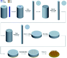
Polymethylmethacrylate (PMMA) composite fibers with micro/nanowire arrays of polystyrene (PS) fibers embedded were prepared by an iterative melt co-drawing and bundling technique. With section-cutting of the PMMA/PS fiber and the dissolution of inner PS, porous PMMA templates were obtained. The pore diameters and spacings of the template can be controlled by this method. The optical microscopy and scanning electron microscopy (SEM) pictures showed that the diameters of the pores were several microns and the spacings of pores were several tens of microns after the second drawing step. The diameters of the pores after the third drawing step were about 310 nm, and the spacings of pores were 2.30 μm. Then, size control of the Cu micro/nanowire arrays could be achieved by electrochemical deposition technology using this template. The SEM results indicated that the obtained diameters and spacings of the Cu micro/nanowires were in accordance with the size of the template. The obtained lengths of the Cu microwires could reach about 30 μm, which depended on the thickness of the PMMA template and parameters of the electrochemical deposition. Significantly, owing to the simple process and good controllability, various micro/nano array materials can be designed and constructed according to the application requirements by using this method.
Current methods used to produce nanowire arrays include template and non-template methods. Advantages and tradeoffs exist with each method. For example, electrochemical deposition or chemical vapor deposition on the porous anodic aluminum oxide (AAO) template is a conventional method for fabricating ordered nanowire arrays, but it can merely get nanoscale structure, and the spacings of pores of the AAO template are usually less than four hundred nanometers, which limits its application in various scale functional materials.20–28 Noble metal directional catalytic etching combines with photoetching method can produce highly controlled micro/nanostructure,29–32 but the processing cost is considerably high and it can only be used to produce silicon structure. Bayindir group has reported the fabrication of arrays of ordered long nanowires and nanotubes in a flexible polymer fiber by fiber co-drawing method. It can provide excellent controls over the diameter, length and interwire spacing of micro/nanowires. But it cannot produce high-melting-point alloy or metallic nanowires array directly. All their works are focused on the fabrication of aligned long multimaterial multifunctional fibers.33–36 Of course, current fiber drawing techniques can produce metallic micro/nanowires at high temperature with a fiber drawing tower, but the material systems and working conditions have very rigorous criterias.37–39 In a recent paper40 we implement a composite fiber melt-codrawing and bundling method to fabricate micro/nano porous polymer templates with controllable structure size (diameter, spacing, and length). The method mainly involves three steps: preparation of polymer composite fibers, section-cutting to obtain slices with array structure, and dissolving to obtain porous polymer templates. There are some unique advantages about this method. Firstly, cheap materials are processed in economic way. Secondly, the size and position of the micro/nano structure can be macroscopically manipulated. Thirdly, the process aligns all the fibers with the same global orientation. All of these endow the porous polymer template with high-throughput, designability, and high-repeatability.
However, some key problems have not been solved in our previous work. For instance, the template cannot be completely removed and the Cu nanowires with complete structure have not been obtained. In the present work, we choose another material system of PMMA/PS to prepare the porous PMMA template due to the good solubility of PMMA at room temperature. Based on this material system, the effect of the dissolving process on the morphology of Cu micro/nanowires is relatively weak and the Cu micro/nanowires with complete structure can be obtained by common electrochemical deposition method. In the case, the structure size of porous PMMA template and prepared micro/nanowires can be controlled conveniently by this method.
![]() | ||
| Fig. 1 Schematic illustrations of the fabrication procedures for porous PMMA template and Cu micro/nanowire arrays. | ||
Then the porous PMMA template was used to make Cu micro/nanowire arrays by electrochemical deposition technology. Firstly, the substrate Au film was deposited on one side of the template via magnetron sputtering in vacuum with the thickness about 1 μm at 1.0 × 10⁻⁴ Pa and 40 W for 2 hours. Then, the thickness of the substrate was increased to 10 μm by electrochemical deposition of a Cu film in order to reinforce the substrate. A 500 ml de-ionized water solution of the electrolyte included 100 g CuSO4, 30 g H2SO4, 49.5 mg NaCl, 0.2 ml New Kotic-A, 2 ml New Kotic-C.
A conducting wire was bonded on the film to serve as an electrode. Then, the sample was fixed on the quartz slide, the sample was covered with insulating tape and one side of the template was in exposure without the film. After this, the sample on the slide was dipped into the electrolyte mentioned above and the electrochemical deposition was carried out at 1–2 V vs. SCE and 1 Hz DC pulse. After 200–500 s, the electrochemical deposition process was terminated. Then the Cu micro/nanowire arrays were obtained after dissolving PMMA template in tetrahydrofuran solution.
Fig. 2 shows the relationships of shear viscosity and shear rate for PS and PMMA at 220 °C, 230 °C and 240 °C, respectively. With increasing shear rate, the shear viscosities of PS and PMMA decreased, representing typical “shear thinning” effect, which was conducive to the fiber drawing process. The shear viscosity of PMMA decreased obviously with increasing temperature and was gradually close to the shear viscosity of PS at low shear rate region. It was found that the unsteady flow phenomenon happened and the fiber surface showed zigzag structure at 220 °C drawing, probably due to that their viscosities were higher and they were not close to each other. The fiber was easy to break at 240 °C drawing, probably due to their lower viscosities. At 230 °C drawing, the fiber surface was smooth and the drawing process was steady, probably due to that the shear viscosities of PS and PMMA were close to each other at low shear rate region. Moreover, in combination of the relationship of the feeding speed and the fiber diameter, we identified the optimum processing conditions. The shear viscosity of the core material PS was 3.94 × 10² Pa S drawing at 230 °C, 2.88 × 10² s−1, while 4.84 × 10² Pa S of the outer layer material PMMA under the same experimental conditions.
![]() | ||
| Fig. 2 The relationship of shear viscosity and shear rate for PS and PMMA at 220 °C, 230 °C and 240 °C. | ||
In our experiment, the length of the preformed rod used in the first drawing step was about 100 mm, the machined thick-wall PMMA tube used for preformed rod preparation had 9 mm outer diameter, 900 μm inner diameter and about 4 mm wall thickness, the size of the PS rod that could be inserted into the thick-wall PMMA tube matched with the size of the center hole of the PMMA tube. The outer diameter and wall thickness of the thin-wall PMMA tube used for fibers bundling before the second and the third drawing steps were 9 mm and 750 μm, respectively. The size of the PMMA/PS fibers should be above 500 μm in diameter and about 50 mm in length, so they were strong enough to be handled and stacked in good order in the thin-wall PMMA tube. Actually, about 200 PMMA/PS fibers were stacked inside the thin-wall PMMA tube and the fibers spontaneously arranged as hexagonal lattices inside the tube due to uniform fiber diameter.
The factors that influence the size reduction ratio (λ) include the outer diameter of the preformed rod (D1) and the fiber (D). Here, λ is defined as λ = D1/D. The diameter of the fiber is determined by the diameter of the extrusion die, the feeding speed and the drawing speed. The structure of the template depends on the size of preformed rod including the diameter of the PS rod (D2) and the PMMA tube. The simple relationship is that the pore diameter over the spacing equal to the ratio of D2 to the difference between D1 and D2. At the drawing step of “n”, the pore diameter plus the spacing equal to the ratio of D1 to λn. According to these simple relationships, we obtained the theoretical values of each drawing step shown in Table 1. Starting from the 900 μm inner diameter and 9000 μm outer diameter of the preformed rod, the diameters of the obtained pores would decrease to 60.00 μm, 4.00 μm and 0.27 μm, and the spacings of pores would decrease to 540.00 μm, 36.00 μm and 2.40 μm after the first, the second and the third drawing steps, respectively.
| Sample | Outer diametera (μm) | Pore diameter (μm) | Design pore diameter (μm) | Spacing (μm) | Design spacing (μm) |
|---|---|---|---|---|---|
| a Both the outer diameter and the size about preformed rod were measured by vernier calipers. The pore diameter and spacing about fiber of step 1 and fiber of step 2 were measured by optical microscope. The pore diameter and spacing about fiber of step 3 were measured by SEM. | |||||
| Preformed rod | 9000 | 900 | 900.00 | — | — |
| Fiber of step 1 | 600 | ∼60 | 60.00 | ∼540 | 540.00 |
| Fiber of step 2 | 600 | ∼4.4 | 4.00 | ∼31 | 36.00 |
| Fiber of step 3 | 600 | ∼0.31 | 0.27 | ∼2.30 | 2.40 |
The experimental values of the samples obtained from optical microscope and SEM images are also listed in Table 1. Starting from the inner diameter of about 900 μm, the diameters of the PS cores became nearly 60 μm after the first drawing step with a size reduction ratio of 15. After the second drawing step, the diameters of the pores were reduced to 4.4 μm, and the spacings of adjacent pores were about 31 μm with the same size reduction ratio. The drawing step was repeated a third time with the fibers obtained from the previous steps to obtain nanometer-sized structure. This third step reduced the pores diameters to about 0.31 μm, and the spacings of adjacent pores were about 2.30 μm. The experimental results are well followed the design values under the same processing condition, which demonstrates the size controllability of the porous template by using this method. Actually, the total number of iterative steps, the number of packed fibers and how tightly they packed together after each drawing step are all greatly influencing the ultimate size of the template. Optical image of the fabricated fiber is shown in Fig. 3.
Fig. 4(a) is the optical microscope image taken at the cross section of the fiber obtained from the second drawing step after removing PS. It can be seen that the pores distribute uniformly and form ordered hexagonal array in the PMMA matrix. The size distribution of the pores obtained from the second drawing step is shown as a histogram in Fig. 4(b), in which 84% pores are found to be 4.4 ± 0.3 μm, corresponding to ±6% variation in diameter. The size distributions of 92% spaces of pores are found to be 31 ± 3 μm, corresponding to a ±9% variation (Fig. 4(c)). Factors contributing to the size distribution are slight variations in the composite fibers from the first drawing step. The PMMA/PS preformed rod was heated uniformly in the furnace of the capillary rheometer during the extrusion process, so the heating time varied with the different parts of the preformed rod. As a result, the diameter of the PS core was decreased gradually with the increase of drawing time. Relevant optimization studies will be done in the future by carefully selection of the fibers or using a special drawing tower that consists of a thermally isolated double zone furnace.
![]() | ||
| Fig. 4 (a) Cross-sectional optical microscope image of the second step PMMA template after removing PS, (b) the size distribution of pores and (c) the spaces of pores. | ||
Fig. 5(a) is the SEM image taken at the cross section of the fiber obtained from the third drawing step. We can see the structural integrity of the pores is well conserved after removing PS. Also the surface of the PMMA template of the third step is fairly smooth. The result is much better than that of the PE template obtained in our previous work,40 which is benefiting for the subsequent experimental processes and its practical application. Moreover, most of the pores have round shapes, around which the shearing deformations induced by section-cutting process are very small, seen the individual pore in Fig. 5(b). However, the shearing deformations cannot be completely avoided causing the shape of a very few pores not perfectly round. It can be seen that the sizes of the pores are not very uniform. Factors contributing to the size distribution are variations in the composite fibers from each previous drawing steps, as mentioned above. The size distribution of the pores obtained from the third drawing step is shown as a histogram in Fig. 5(c), in which 83% pores are found to be 310 ± 30 nm, corresponding to ±9% variation in diameter. The size distributions of 96% spaces of pores are found to be 2.3 ± 0.5 μm, corresponding to a ±21% variation (Fig. 5(d)).
![]() | ||
| Fig. 5 (a) Cross-sectional SEM image of the third step PMMA template and (b) individual pore after removing PS, (c) the size distribution of pores and (d) the spaces of pores. | ||
The obtained porous PMMA templates from the second and the third step PMMA/PS fibers were used to prepare Cu micro/nanowires by electrochemical deposition method. The SEM image of Cu microwires after removing the PMMA template obtained from the second step PMMA/PS fiber is shown in Fig. 6(a). High-resolution SEM images indicates that the surface of substrate is smooth after removing PMMA, and the shape of microwires are regular and integrated. The obtained diameters of the Cu microwires are about 4–5 μm and the spacings are about 30 μm, which are in accordance with the size of the template. The Cu microwires grew along the surface of the pore channels forming hollow structure because the pores in the template were not covered completely by the substrate materials during the magnetron sputtering process. We believe the size of the pores and the parameters of the electrochemical deposition process have a significant impact on the microwires shape. The EDX spectrum collected on a microwire (Fig. 6(b)) confirms that the microwire is mainly made of copper (Fig. 6(c)). Fig. 7 shows the Cu microwires of different samples with different electrochemical deposition processes. The obtained lengths of the Cu microwires are nearly 15 μm, seen in Fig. 7(a), and the obtained lengths of the Cu microwires are nearly 30 μm approaching the thickness of the PMMA template, seen in Fig. 7(b). The length of the Cu microwires mainly depends on the thickness of the template and the parameters of the electrochemical deposition process. Theoretically, metallic microwires with ultrahigh aspect ratio can be realized by this method. We can also notice the slight differences in diameters, shapes, and inclination angles of the Cu microwires due to the pore size differences and deformations during sample preparation process. Therefore, the key to achieving uniform Cu micro/nanowires is preparing a template with uniform pore structure, which will be an important task in future research.
![]() | ||
| Fig. 6 (a) SEM image of Cu microwires and (b) the individual Cu microwire after removing the PMMA template obtained from the second step PMMA/PS fiber, (c) the according EDX spectrum. | ||
The SEM image in Fig. 8(a) shows Cu nanowires after removing the PMMA template obtained from the third step PMMA/PS fiber. From the tilted image, the diameters, spacings and lengths of the Cu nanowires are about 300 nm, 2–3 μm and 2–3 μm, respectively. Most of the nanowires show integrated structure and uniform distribution. Some of them are broken probably during the dissolving or other operating processes. This cannot be avoided totally but can be improved by optimizing the electrochemical deposition parameters and increasing the operating area of the template, which will be carried out in the next work. From the fracture surface morphology of the nanowires, it can be seen that the Cu nanowires also have hollow structure. Fig. 8(b) shows the XRD pattern of the Cu nanowires after removing the Cu substrate as an example. The inset includes the highest peak corresponding to (111) of the Au substrate, after removing the highest Au peak, it can be seen clearly that the four peaks located at 2θ of 43°, 50°, 74° and 90° are corresponding to (111), (200), (220) and (311) of Cu, respectively, while the additional peaks at 2θ of 38°, 44°, 64°, 77° and 81° correspond to (111), (200), (220), (311) and (222) of the Au substrate, respectively. It can be seen clearly that the intensity ratio of (111) peak to other peaks of Cu is stronger than that of the powder sample when compared to JCPDS card for Cu (no. 04-0836), which indicates that the nanowires have preferred (111) crystal orientation.
![]() | ||
| Fig. 8 (a) SEM image of Cu nanowires after removing the PMMA template obtained from the third step PMMA/PS fiber, (b) the according XRD pattern. | ||
These experimental results demonstrate that the use of this PMMA template is highly promising for the preparation of metallic micro/nanowire arrays with desired sizes. Further work will focus on preparing the porous PMMA template with different sizes, including different pore diameters and spacings, increasing the effective area and the aspect ratio of the metallic micro/nanowire arrays, further optimizing the structural integrity of the polymer template and the obtained micro/nanowires.
Footnote |
| † Electronic supplementary information (ESI) available. See DOI: 10.1039/c6ra15837d |
| This journal is © The Royal Society of Chemistry 2016 |