Structural, optical and photo-electrochemical properties of hydrothermally grown ZnO nanorods arrays covered with α-Fe2O3 nanoparticles

Mohua Chakrabortya, Dhrubojyoti Royb, Amrita Biswasc, R. Thangavel*a and G. Udayabhanuc
aSolar Energy Research Laboratory, Department of Applied Physics, Indian School of Mines, Dhanbad 826 004, India. E-mail: thangavel.r.ap@ismdhanbad.ac.in; rthangavel@gmail.com
bSamtel Centre for Display Technologies, Indian Institute of Technology, Kanpur, Uttar Pradesh 208 016, India
cDepartment of Applied Chemistry, Indian School of Mines, Dhanbad 826 004, India

Received 17th June 2016 , Accepted 2nd August 2016

First published on 2nd August 2016


Abstract

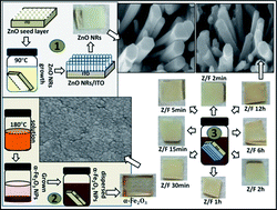
A low cost hydrothermal method and subsequent wet-chemical process has been used for the preparation of a ZnO nanorod (NR) array film grown on tin doped indium oxide (ITO) coated glass substrates, post decorated by α-Fe2O3 nanoparticles (NPs). The effect of the amount of α-Fe2O3 NPs on the properties of ZnO NRs such as electron scattering, surface roughness, photo-charge transport and interface recombination has been investigated. Furthermore, the optimized α-Fe2O3 NPs@ZnO exhibited enhanced light absorption, charge separation and charge transport properties, as characterized by UV-vis absorption spectra and the photo-electrochemical characterization by Linear Sweep Voltammetry (LSV) and Electrochemical Impedance Spectroscopy (EIS). An optimum amount of α-Fe2O3 NPs on the ZnO NRs enhanced the photocurrent density by 163% and the photo-conversion efficiency by more than 2.5 times compared to those of the bare ZnO NRs. These results indicated that the prepared α-Fe2O3 NPs@ZnO NRs could serve as an efficient photo-electrode material for photo-electrochemical cells.


Introduction

Photo-electrochemical cells using nano-structured semiconductors offer great potential for converting solar energy to a storable and clean chemical energy.1–5 A large number of semiconductor materials like metal oxides and sulphides (i.e.; TiO2, ZnO, α-Fe2O3, ZnS, CdS) have been identified as active photo-electrode materials for photo-electrochemical (PEC) applications.6–10 In the past decade, zinc oxide (ZnO) and hematite (α-Fe2O3) have been widely used as photo-catalysts/photo-electrodes due to their low cost, abundant availability and non-toxicity.11–14 ZnO has attracted extensive interest due to its wide band gap (Eg = 3.37 eV), large exciton binding energy (60 meV) and high carrier mobility (∼205–1000 cm2 V−1 s−1) but this wide band gap has limited its absorption for the required band gap excitation and charge carrier generation within the UV range of light.15 Whereas, α-Fe2O3 is another promising material with visible light active narrow band gap (Eg = 2.22 eV), outstanding photoconductivity and photovoltaic properties16 but the small diffusion length (2 to 4 nm) of minority carriers in this material could limit its effective thickness and light absorption.17 On the basis of these concerns, many investigations had been targeted on ZnO/α-Fe2O3 composite nanostructure to provide an alternative route to band gap engineering, for compensating individual material limitations and disadvantages.18–20 Li et al.21 had also expected enhanced ability of broader light absorption and more efficient electron–hole separation in the ZnO/α-Fe2O3 hetero-nanostructure. After that, Liu et al.22 had reported the synthesis of ZnO/α-Fe2O3 nanotube (NT) composites using a low-temperature hydrothermal and photochemical deposition process and presented a great improvement in photo-catalytic characteristics compared to the bare ZnO NRs. According to literature survey, it can be observed that it is very difficult to grow ZnO/α-Fe2O3 nanowires (NWs) thin films by using a simple wet chemical process due to dissolving behaviour of ZnO.23 As Guo et al.24 had used simple wet chemical process and immersed ZnO NW array in aqueous iron chloride solution and had calcined and grown ZnO/ZnFe2O4 core–shell NW arrays. This group had also explained that the use of iron chloride solution on ZnO NRs shows hydrolysis of Fe3+ ions on the surface of ZnO NWs leads to the formation of Fe (OH)3 shell at the expense of ZnO and further annealing provide ZnO/ZnFe2O4 core–shell NW arrays. It had been reported that a controllable chemical composition and annealing can tune ZnO NWs to form stoichiometric ZnFe2O4 to ZnFe2O4/α-Fe2O3 composite, and eventually to α-Fe2O3 NTs.25 Many reports revealed that the dissolving ability and reactivity of ZnO, can easily form ZnO/ZnFe2O4 by using iron precursors with wet chemical methods24–26 but it is very complicated to grow α-Fe2O3@ZnO NRs thin films with these wet chemical methods.

In this work, we have proposed an easy and low cost method for fabrication of α-Fe2O3 as a shell layer on the surface of ZnO NWs as a core–shell nanostructured electrode for PEC solar cell application. The ZnO NRs on conducting substrate and α-Fe2O3 NPs have been prepared by low cost hydrothermal method and the hetero-junction have been prepared by simply dipping ZnO NRs into α-Fe2O3 NPs dispersed solution. The α-Fe2O3 NPs coupled ZnO core–shell NRs hetero-structures can enhance the separation of photo-induced electron–hole pairs, leading to improved photo-electrochemical properties. The surface morphology, optical property, photocurrent, and photo-electrochemical activity of these hetero-structured photo-electrodes under visible light irradiation have been studied.

Experimental details

Preparation of ZnO NRs

A general concept of fabrication of ZnO NRs on ITO coated glass substrates based on a two step process has been used.27 At first zinc acetate dihydrate was dissolved in 2-methoxyethanol and monoethanolamine (MEA) and stirred at 60 °C for 2 hours to prepare the seed solution. The molar ratio of MEA to zinc acetate dihydrate was maintained at 1.0 and the concentration of zinc acetate was 0.5 M. The obtained sol was aged for 24 h at room temperature. The seed solution was coated on the cleaned ITO coated glass substrate by spin coating. After spin coating, substrate was dried at 300 °C for 10 min on a hot plate to evaporate the solvent and remove organic residuals. The procedure for coating to drying was repeated four times. Then the film was annealed at 500 °C for 1 h to create a crystalline ZnO seed layer. In the second step, ZnO NR arrays were grown on the substrate by using the hydrothermal method. The modified substrates were immersed in the aqueous solution containing zinc nitrate hexahydrate and hexamethylenetetramine at 90 °C for 5 hours. The grown films were washed with distilled water and then dried at room temperature.

Preparation of α-Fe2O3 NPs

A typical synthesis procedure for preparation of hematite NPs has been adopted.28 Iron chloride hexahydrate as starting precursor and sodium oleate/oleic acid as capping reagents were used. For synthesis, sodium oleate and a mixture solution composed of ethanol and oleic acid were added subsequently to an aqueous solution of iron chloride in a Teflon-lined stainless autoclave under stirring at room temperature. After 2 h, a fizzy organic layer appeared on the upper part of the reaction mixture. The autoclave was sealed and treated at 180 °C for 12 h and then cooled to room temperature. The precipitate was collected by centrifugation and washed with ethanol. The as-synthesized product was dispersed in cyclohexane (10 ml) and centrifuged at a high speed (7000 rpm) to remove any insoluble precipitate. The red and transparent colloidal solution of hematite NPs was collected and re-dispersed in cyclohexane.

Preparation of ZnO@α-Fe2O3 core–shell NRs

In order to cover the ZnO NRs α-Fe2O3, ITO/ZnO NRs samples were placed upside down in the synthesized re-dispersed hematite solution for different deposition time (2 min, 5 min, 15 min, 30 min, 1 h, 2 h, 6 h, 12 h) to obtain different layer thickness. Moreover, placing the samples upside-down was for preventing the samples from attachment of large particle clusters. The substrate was washed with distilled water and then dried at room temperature. ZnO@α-Fe2O3 core–shell NRs were fabricated as an oxide–oxide heterojunction for photo-electrochemical applications. In order to extract the individual morphological and absorption property in grown α-Fe2O3 NPs, α-Fe2O3, thin films were deposited by simply immersing cleaned ITO coated glass substrates in the as-prepared α-Fe2O3 NPs dispersed solution, washed with DI water and dried at room temperature. The success of preparation of ZnO NRs, α-Fe2O3 NPs and α-Fe2O3 NPs coating on ZnO NRs has been indicated by the visual colour change as shown in Fig. 1. As the samples grown with different deposition time i.e. 2 min, 5 min, 15 min, 30 min, 1 h, 2 h, 6 h and 12 h; are here after named as Z/F2 min, Z/F5 min, Z/F15 min, Z/F30 min, Z/F1 h, Z/F2 h, Z/F6 h and Z/F12 h, respectively.
image file: c6ra15752a-f1.tif
Fig. 1 A schematic demonstration of preparation of ZnO NRs, α-Fe2O3 NPs, α-Fe2O3@ZnO NRs and the photos of α-Fe2O3 NPs, bare ZnO nanorods (NRs) and the decorated with α-Fe2O3 NPs with various duration thin films.

Characterization

The crystal phases of the samples were characterized using X-ray diffraction (XRD) (Bruker D8 Advance Diffractometer) with monochromatic Cu-Kα1 radiation (λ = 1.5406 Å). Raman spectra were recorded on a micro-Raman setup from Renishaw, UK, equipped with a grating of 2400 lines/mm and a Peltier cooled CCD. The GRAM-32 software was used for data collection. A microscope from Olympus (Model: MX50 A/T) was attached to the spectrometer, which focuses the laser light onto the sample and had collected the scattered light at 180° scattering geometry. The 514.5 nm line of argon ion laser was used as an excitation source. The microstructural features of the sample were detected using a ZEISS Supra 55 Field Emission Scanning Electron Microscope (FESEM) and Bruker Dimension Icon Atomic Force Microscope (AFM), respectively. Elemental analysis was carried out using Energy-Dispersive X-ray Spectroscopy (EDXS). To measure the light absorbance of the sample an Agilent Cary 5000 UV-Vis-NIR double beam spectrophotometer was used. Photoluminescence spectroscopy at room temperature was carried out using a Hitachi f-2500 spectrophotometer. The current–voltage measurement was carried out using a Keithley 2450 source meter and to determine the photo-response behaviour, a solar simulator with the illumination intensity of one Sun (AM 1.5, 1 kW m−2, NCPRE IIT Bombay) was used as a light source for light illumination. Electrochemical measurements were conducted on a CHI660C electrochemistry workstation at the Department of Applied Chemistry, Indian School of Mines, Dhanbad.

Results and discussions

Structural characterization of α-Fe2O3@ZnO NRs based thin films

The XRD patterns of ZnO NRs and α-Fe2O3@ZnO NRs grown on ITO substrates have been presented in Fig. 2. The standard patterns with pure phase wurtzite ZnO (PDF 36-1451, black line) with rhombohedral structure of hematite (PDF 33-0664, red lines) have been used for comparison. This indicates that the grown bare ZnO NRs have the hexagonal wurtzite structure with high crystallinity. The higher peak intensity along (002) plane verify the preferred orientation of growing ZnO NRs along c-axis. After coating hematite (α-Fe2O3) NPs, the apparent diffraction peaks of hematite have been observed at all α-Fe2O3@ZnO NRs samples. However, the diffraction peaks of hematite have weaker peaks than those corresponding to bare ZnO NRs.29,30 Therefore, the diffraction peaks of hematite could be detected clearly only in long duration grown samples, i.e. Z/F6 h and Z/F12 h. Furthermore, the inset XRD patterns in Fig. 2 show the comparison of the magnified peak patterns before and after coating with α-Fe2O3.
image file: c6ra15752a-f2.tif
Fig. 2 XRD patterns of as prepared ZnO NRs and α-Fe2O3@ZnO NRs. The inset shows magnified XRD pattern of ZnO NRs, before and after α-Fe2O3 sensitization.

In addition, in order to obtain a qualitative idea about the sensitization effect of α-Fe2O3 NPs on ZnO NRs we have carried out Raman analysis. The wurtzite type of ZnO belongs to P63mc space group and possess nine optical phonon modes near the centre of the Brillouin zone (Γ), which can be given by the irreducible representation Γopt = A1 + 2B1 + E1 + 2E2. In these optical phonon modes, B1 modes are usually Raman inactive and the remaining modes are Raman active. The polar A1 and E1 each splits into two modes, as longitudinal optical (LO) and transverse optical (TO) modes. The non-polar E2 modes have two components E2low and E2high associated with Zn and O atoms sub lattices, respectively.31

The Raman spectra of as grown naked ZnO NRs and α-Fe2O3@ZnO NRs have been presented in Fig. 3. In all spectra, the characteristic structure of ZnO could be observed with a strong E2high mode at ∼437 cm−1 associated with an A1TO mode at ∼380 cm−1 and E2high − E2low second order mode at 330 cm−1.31,32 The other Raman bands appeared around 580 cm−1 and 1150 cm−1 correspond to 1 LO and a second order 2 LO phonon modes. Generally, these LO phonon modes of wurtzite ZnO formed due to A1LO and E1LO phonon modes which have been appearing as a single (quasi LO) mode. This quasi mode has appeared as two bands in all the samples.32 Whereas hematite belongs to crystal space group with different typical Raman active modes. Here a successful coating of α-Fe2O3 NPs on ZnO NRs has been characterized by the peaks at around 225, 477 (A1g symmetric stretching mode), 299, 412 (Eg symmetric bending mode) and 1317 cm−1[thin space (1/6-em)]33,34 along with characteristic peaks of ZnO in all coated samples. The bands at 1317 cm−1 can be ascribed to two Magnon scattering.35 In the spectra different intensities were present because of the different thicknesses of α-Fe2O3 coating, but there was no evidence of Raman shifts in these bands.


image file: c6ra15752a-f3.tif
Fig. 3 Raman spectrum of as prepared ZnO NRs and α-Fe2O3@ZnO NRs.

Morphology of α-Fe2O3@ZnO NRs thin films

The unmodified ZnO NRs and α-Fe2O3 NPs modified ZnO NRs have been analyzed by FESEM and AFM to investigate the surface morphology and roughness. In Fig. 4(a)–(j) the FESEM images show the top-view and zoomed view of ZnO NRs, α-Fe2O3 NPs, α-Fe2O3@ZnO NRs deposited and grown on ITO coated glass substrates. The grown ZnO NRs [Fig. 4(a)] are vertically oriented, well aligned hexagonal structure of almost uniform size with smooth surface. The diameter and height of the NRs have been estimated for all samples [using ImageJ software] are in the range of 200–300 nm and <2 μm, respectively. Fig. 4(b) shows that α-Fe2O3 NPs are distributed homogeneously throughout the film with size around 7 nm. Fig. 4(c)–(j) shows small, uniform particles of α-Fe2O3 are distinctly deposited on ZnO NRs substrates. The FESEM and AFM (Fig. S1(a)–(I)) investigations revealed, the amount of α-Fe2O3 NPs effectively covered the surfaces of ZnO NRs in proportion to dipping duration and formed a uniform layer. The ZnO NRs surface totally covered by α-Fe2O3 NPs becomes slightly rounded compared to the hexagonal shape of bare ZnO NWs but the clusters of α-Fe2O3 NPs were not quite uniform. After sensitization of α-Fe2O3 NPs up to 1 hour, the surface of each NRs became rough and diameter increased largely but made the film surface smoother (Table S1) compared to unmodified ZnO NRs samples. The smoothing of the surface of the film arises as sensitization of NPs reduces the gaps between NRs.36,37 Whereas, further modification of ZnO NRs has been done with α-Fe2O3 NPs up to 12 hours and which resulted in a significant increase in film surface roughness as rough NPs fully covered the surfaces of ZnO NRs.37 At the same time we have performed an EDXS analysis to determine the kinds of elements in α-Fe2O3@ZnO NRs. In the spectra of Fig. 4(k), intense signals for Zn, O and weak signals from Fe are observed indicating that the Fe contained NPs has been successfully loaded onto the ZnO NRs. The other observed peaks correspond to the ITO coated glass substrates and platinum coating.
image file: c6ra15752a-f4.tif
Fig. 4 FESEM images of (a) bare ZnO NRs, (b) α-Fe2O3 NPs, (c) Z/F2 min, (d) Z/F5 min, (e) Z/F15 min, (f) Z/F30 min, (g) Z/F1 h, (h) Z/F2 h, (i) Z/F6 h, (j) Z/F12 h thin film samples, (k) EDX spectrum of Z/F15 min sample.

Optical properties of α-Fe2O3 NPs@ZnO NRs thin films

Optical properties of semiconductors have an important role in the photo-electrochemical solar cell. Fig. 5 shows the optical absorption spectra of as prepared films. As visible, the absorption edge of bare ZnO NRs and α-Fe2O3 NPs based thin films were at about 390 nm and 520 nm, respectively. Whereas the ZnO/α-Fe2O3 heterostructures show an obvious red shift compared to bare ZnO NRs (up to 500 nm maximum). With increase in α-Fe2O3 layer thickness in the heterostructures, it has been observed that ZnO NRs/α-Fe2O3 NPs have higher absorption in the visible light as compared to ZnO as expected. Additionally, the band gap of ZnO and α-Fe2O3 calculated from the Tauc's plot of ZnO and α-Fe2O3 (presented as the inset of Fig. 5) are 3.16 eV and 2.08 eV, respectively.38,39 The spectra of ZnO NRs/α-Fe2O3 NPs revealed an evidence of low-energy absorption tail (Urbach tail) caused by the formation of new localized energy levels (new interface energy states) close to the conduction band in forbidden band gaps.40 Also in such energy states the electrons' lifetime can be effectively hamper the recombination. Therefore, it could be interesting to characterize the influence of these interface energy states with photoluminescence (PL) and photo-electrochemical properties.
image file: c6ra15752a-f5.tif
Fig. 5 UV-vis absorption spectra of bare ZnO, α-Fe2O3 and all α-Fe2O3@ZnO NRs films. The inset shows Tauc's plot for ZnO and α-Fe2O3.

PL emission spectroscopy is useful to explain the migration, transfer and recombination processes of the photogenerated electron–hole pairs in the semiconductors. This PL emission observed due to recombination of excited electrons and holes. Therefore, a stronger PL intensity results from more recombination probability of electron-holes. Fig. 6 shows a comparison of ZnO NRs, α-Fe2O3@ZnO NRs thin film samples with excitation at 320 nm. From the spectra it has been observed that the PL intensity decreased dramatically when α-Fe2O3 was coupled with ZnO and the results indicates the formation of heterojunction between α-Fe2O3 and ZnO. These results show a decrease in the rate of recombination of photo-induced electrons and hence weakening the PL intensity.41 The photo-generated electrons can easily migrate from α-Fe2O3 surface of the ZnO conduction band due to its potential difference at α-Fe2O3@ZnO interface. The observed PL intensity has been found to decrease and the lowest was observed for Z/F1 h. After that in case of Z/F2 h, Z/F6 h and Z/F12 h, the PL intensity increased, which specify that more layer of α-Fe2O3 NPs have enhanced recombination effect.42,43 It indicates that an optimized layered heterostructure Z/F15 min, Z/F30 min, Z/F1 h could effectively hinder the recombination of photo-generated charge carriers, which are helpful for the separation of the photo-generated electron–hole pairs.


image file: c6ra15752a-f6.tif
Fig. 6 The photoluminescence spectra of bare ZnO and all α-Fe2O3@ZnO NRs films.

Electrical characterization

Electrical properties of α-Fe2O3@ZnO NRs, which has been measured with current–voltage characterization. Fig. 7 shows the current density vs. voltage (JV) curves of all grown samples under darkness and illumination within voltage range −5 V to +5 V. These variations in current density may be caused by surface roughness and quantity of sensitized α-Fe2O3 NPs on ZnO NRs. The figure shows lower dark, photocurrent densities for bare ZnO NRs samples as the ZnO is highly resistive and UV light active material. The sensitization with conductive α-Fe2O3 NPs (up-to 1 h) show an enhancement in dark current density compared to bare ZnO, whereas the light illumination show more increase in current density due to improved photo-electron transfer between α-Fe2O3 NPs and at α-Fe2O3 NPs@ZnO NRs interface. The variation in dark, photocurrent density with sensitization of α-Fe2O3 NPs have been explained through a schematic of expected electron transport at α-Fe2O3 NPs loaded ZnO NRs [Fig. 8]. The light illumination on α-Fe2O3 NPs formed photo excited electron–hole pairs and the suitable interface band alignment could transfer the photo-electrons to ZnO and has enhanced current density. The sensitization of the large amount of conductive α-Fe2O3 NPs has created more electron–hole pairs and transferred photo-electrons to the interface and has enhanced the current density but may promote recombination effects also. Therefore, a different character of electron transport has been observed with long duration sensitized samples. In Z/F2 h, Z/F6 h and Z/F12 h samples, the increase in the layer of NPs and surface roughness has dominated the electron scattering by reducing their mean free path lengths and thus has decreased the dark current density [(ref. 44), Fig. 8]. The illumination of these samples suffers more recombination and decreased photo-electrons transportation with increased surface roughness and loading, high amount of NPs.42,43 The reason for higher recombination may be due to band alignment at α-Fe2O3/ZnO interface. The conduction band (CB) of α-Fe2O3 has little lower potential than that of ZnO,22 so only highly energetic photo-electrons were able to reach the interface to populate at the CB of ZnO. The increased layer of sensitized NPs has blocked the flow of high energetic photo-electrons to the interface and recombined with holes which account for the reduction of electrons from α-Fe2O3 to the 1D ZnO nanorods. Therefore, the samples Z/F15 min, Z/F30 min and Z/F1 h have shown better photo-response characteristics compared to the others due to a reduced recombination effect (as observed in PL measurement). The observed photo-current density and their respective enhancement in current density under illumination for all samples have been listed in Table 1.
image file: c6ra15752a-f7.tif
Fig. 7 Current density vs. voltage measurements of bare ZnO and all α-Fe2O3@ZnO NRs films under dark and visible light illumination at room temperature.

image file: c6ra15752a-f8.tif
Fig. 8 Schematic of electron transport in all grown thin film samples (at top). Proposed process schematic of transfer and separation of visible-excited high-energy electrons in the α-Fe2O3–ZnO heterostructure (left bottom).
Table 1 Photocurrent density and enhancement in current density (δ) with illumination observed from IV and LSV measurements. Impedance parameters derived from the equivalent circuit for the α-Fe2O3@ZnO samples
Sample J at +5 V (mA cm−2) from IV curve δ (%) in IV

image file: c6ra15752a-t1.tif

J at +1.0 V (mA cm−2) from LSV curve δ (%) in LSV

image file: c6ra15752a-t2.tif

Rs (Ω) R1 (Ω) R2 (Ω)
ZnO 0.035 11.42 0.84 4.76 8.378 4.31 × 10⁴ 301.3
ZnO_L 0.039 0.88 10.07 8.50 × 10⁸ 189.4
Z/F2 min 0.563 12.61 1.35 8.14 0.01 2.66 × 10⁵ 140.5
Z/F2 min_L 0.634 1.46 2.03 1.43 × 10² 20.8
Z/F5 min 0.792 8.96 1.42 9.15 10.66 9.67 × 10⁴ 138
Z/F5 min_L 0.863 1.55 13.7 4.70 × 10⁴ 4.039
Z/F15 min 1.124 35.49 1.69 9.46 2.023 5.78 × 10⁴ 50.9
Z/F15 min_L 1.523 1.85 8.004 4.14 × 10³ 5.25
Z/F30 min 1.178 43.87 1.75 20.57 0.1 2.29 × 10⁴ 49.23
Z/F30 min_L 1.695 2.11 0.01 3.58 × 10³ 4.9
Z/F1 h 1.374 53.28 1.89 22.75 30.69 8056 11.02
Z/F1 h_L 2.103 2.32 0.422 2010 2.24
Z/F2 h 1.185 18.64 1.77 11.86 16.34 2.24 × 10⁴ 39.08
Z/F2 h_L 1.406 1.98 4.989 1.45 × 10⁴ 9.83
Z/F6 h 0.405 21.48 1.67 1.19 4.261 2.81 × 10¹³ 12.85
Z/F6 h_L 0.492 1.69 4.069 1.07 × 10¹¹ 10.93
Z/F12 h 0.040 7.5 1.58 1.26 4.989 5.13 × 10¹³ 9.83 × 10¹¹
Z/F12 h_L 0.043 1.60 16.78 9.81 × 10¹³ 4.01 × 10¹⁰


Photo-electrochemical tests

The photo-generation of electron–hole pair and charge separation are the essential conditions required for photo-induced redox reaction by semiconductor electrodes.45 The initiation of redox reaction can occur due to depletion layer in the semiconductor/solution interface and with external biasing. In order to explore the electrochemical behaviour of samples, ZnO NRs, α-Fe2O3@ZnO NRs as photoanodes, a platinum counter electrode and Ag/AgCl reference electrode in 0.1 M NaOH aqueous solution were used as three electrode photo-electrochemical cell.

Linear sweep voltammograms (LSV) is a common electrochemical technique to investigate charge-carrier characteristics of the semiconductor/electrolyte interface. Fig. 9 represents the LSV (IV curves) collected from a bare ZnO NRs array and α-Fe2O3@ZnO heterostructures, with and without illumination, as the function of applied bias potential. For bare ZnO, the dark current density has been observed in the order of 0.84 mA cm−2 and the photocurrent densities show a slight increment. While all samples with α-Fe2O3@ZnO heterostructure showed pronounced photo-response under illumination, which has been attributed to the improved visible light absorption and suitable interfacial charge transport at α-Fe2O3@ZnO heterostructure. Significantly, the Z/F1 h sample showed maximum photocurrent density of 2.32 mA cm−2 at +1.0 V (vs. Ag/AgCl), which is more than 163%, 58.9%, 49.67%, 25.40%, 9.95%, 17.17%, 38.09%, 45% enhancement compared to the bare ZnO (0.88 mA cm−2), Z/F2 min (1.46 mA cm−2), Z/F5 min (1.55 mA cm−2), Z/F15 min (1.85 mA cm−2), Z/F30 min (2.11 mA cm−2), Z/F2 h (1.98 mA cm−2), Z/F6 h (1.68 mA cm−2) and Z/F12 h (1.60 mA cm−2) samples respectively. This photocurrent density was substantially higher than the values recently reported.46 Noticeably, the dark current density and photo-response follows almost the same trend as explained through expected electron transport schematic diagram. The amount of sensitized α-Fe2O3 NPs affected the electron flow and interfacial charge transfer in and between ZnO, α-Fe2O3 nanostructures and oxide–electrolyte interface. Thus the results indicate that Z/F15 min, Z/F30 min, Z/F1 h have higher photocatalytic activity and have better charge transfer/transport rate than that of the other samples, which are due to better photo-conductivity and a faster interfacial charge transfer rate. Since the photogenerated holes reaching the electrode surface participate in the water oxidation reaction, the photo-conversion efficiencies (η%) for PEC water splitting of these photo-anodes have been estimated and presented in Fig. 10 using the same method as in other report.47 The α-Fe2O3 sensitized ZnO NRs samples show better photo-conversion efficiency at 0.39%, 0.42%, 0.50%, 0.53%, 0.45%, 0.38% and 0.35% for Z/F12 h, Z/F6 h, Z/F2 h, Z/F30 min, Z/F15 min, Z/F5 min, Z/F2 min samples, respectively. Whereas, the Z/F1 h NRs sample exhibited optimal photo-conversion efficiency of 0.58%, which was more than 2.5 times than that of the bare ZnO NRs electrode (0.21%).


image file: c6ra15752a-f9.tif
Fig. 9 Photocurrent density (mA cm−2) vs. Ag/AgCl of bare ZnO and all α-Fe2O3@ZnO NRs films under darkness and visible light illumination at room temperature.

image file: c6ra15752a-f10.tif
Fig. 10 PCE (%) for bare ZnO and all α-Fe2O3@ZnO NRs films.

To get further insight into the role of α-Fe2O3 in charge transport process and recombination, the electrochemical impedance spectroscopy (EIS) measurements were carried out at the open circuit potential and frequency range 10 mHz to 100 kHz under dark and illuminated conditions (Fig. 11). The radius of the arc on the EIS spectra is associated with the charge transfer ability of the photoelectrode. The experimental data of Nyquist plots were fitted on a equivalent circuit (inset of Fig. 11) using ZSimpWin 3.22d software. The fitting parameters are shown in Table 1. Generally, the equivalent circuit of such a plot involves inductance (L) attributed to wiring and equipment, sum resistance (Rs), solid electrolyte interface (SEI) resistance, resistance (R1), charge transfer resistance (R2) and a constant phase element Q. Rs included the inbuilt electrode resistance, the electrolyte and the contact resistance formed between the electrode and current collector.48 The variation in the value of the contributed sum resistance (Rs) (Table 1) is not clear as numerous factors are included. R1 represents resistance due to the specific area, morphology and crystallinity of the working electrode, R2 represents the charge transfer resistance between solid–electrolyte interfaces.49 Under dark conditions, compared with plain ZnO NRs array electrode, α-Fe2O3@ZnO NRs (up-to 1 h) array electrode have smaller R2 value (Table 1), thus clearly indicating an enhancement of the charge transfer in each interface (i.e., metal oxide–electrolyte interfaces). The visible response present slightly lower charge transfer resistance in bare ZnO, whereas α-Fe2O3@ZnO NRs (up-to 1 h) show more lower resistance indicating effective photo-charge separation and a faster interfacial charge transfer in the electrolyte. These present disable visible response of pure ZnO and high photo response of sensitized α-Fe2O3 NPs. The expected transport mechanism explained in IV characterization part, which depends on the amount of sensitized α-Fe2O3 NPs show a harmony with observed results in EIS fitted parameters. Whereas, ZnO NRs decorated with more α-Fe2O3 (i.e. Z/F2 h, Z/F6 h and Z/F12 h) suffered with lower interfacial charge transfer and recombination and has endowed the samples with highest R1 and R2. The above photo-electrochemical results convincingly conclude that the α-Fe2O3 layer played positive roles in enhancing the PEC water splitting efficiency of α-Fe2O3NPs@ZnO NRs heterostructure. Therefore, the optimized layer of α-Fe2O3 can improve the interfacial charge transport mechanism and charge recombination possibility in α-Fe2O3NPs@ZnO NRs array electrode.


image file: c6ra15752a-f11.tif
Fig. 11 Nyquist plot of bare ZnO and all α-Fe2O3@ZnO NRs thin films in 0.1 M NaOH aqueous electrolyte solution under dark and visible light illumination conditions. The inset shows the equivalent circuit and Nyquist plot in the lower impedance region.

Conclusions

We successfully fabricated one dimensional vertically well aligned ZnO NRs array followed by modification with different amount of α-Fe2O3 by using the low cost hydrothermal method. As a result of this modification on ZnO NRs array we have obtained visible light photoactive electrodes. Under visible light illumination, the LSV photocurrent density of the ZnO NRs array modified by α-Fe2O3 for 15 minutes, 30 minutes and 1 hour has greatly improved to 1.85 mA cm−2, 2.11 mA cm−2 and 2.32 mA cm−2 which are greater than that of bare ZnO NRs (0.88 mA cm−2) along with PCE of 0.45%, 0.53% and 0.58%, respectively. The α-Fe2O3/ZnO heterojunction array can be used in a photo-electrochemical cell as it has been demonstrated that the α-Fe2O3/ZnO heterojunction array is superior to the ZnO NRs array for photocurrent and photo-electrochemical reaction because of significantly improved charge separation and additional electron supply from α-Fe2O3 to ZnO. The combination of control over coating duration and sensitization to visible light active α-Fe2O3 on ZnO nanowire arrays can act as a promising candidate for photo-electrochemical solar cell.

Acknowledgements

The authors (M. C. and R. T.) would like to acknowledge Dr S. K. Sharma, Department of Applied Physics, Indian School of Mines, Dhanbad for his support to get Photoluminescence measurement. The authors (M. C. and R. T.) acknowledges for the financial support from the Indian School of Mines, Dhanbad, India, for Faculty Research Scheme-FRS (54)/2013-2014/APH, Central Research Facility and Department of Science and Technology (DST) for project with grant number SR/FTP/PS-184/2012, SERB vide Dy. No. SERB/F/5439/2013-14 dated 25.11.2013.

References

  1. J. Tian, Z. Zhao, A. Kumar, R. I. Boughton and H. Liu, Chem. Soc. Rev., 2014, 43, 6920 RSC.
  2. F. Fresno, R. Portela, S. Suarez and J. M. Coronado, J. Mater. Chem. A, 2014, 2, 2863 CAS.
  3. H. Chen and L. Wang, Beilstein J. Nanotechnol., 2014, 5, 696 CrossRef CAS PubMed.
  4. N. Haghighia, Y. Abdia and F. Haghighib, Appl. Surf. Sci., 2011, 257, 10096 CrossRef.
  5. H. Kisch, Angew. Chem., 2013, 52, 812 CrossRef CAS PubMed.
  6. G.-S. Li, D. Q. Zhang and J. C. Yu, Environ. Sci. Technol., 2009, 43, 7079 CrossRef CAS PubMed.
  7. Y. Ling, G. Wang, D. A. Wheeler, J. Z. Zhang and Y. Li, Nano Lett., 2011, 11, 2119 CrossRef CAS PubMed.
  8. D. J. Yang, Z. F. Zheng, H. Y. Zhu, H. W. Liu and X. P. Gao, Adv. Mater., 2008, 20, 2777 CrossRef CAS PubMed.
  9. J. Zhang, Y. Wu, M. Xing, S. A. K. Leghari and S. Sajjad, Energy Environ. Sci., 2010, 3, 715 CAS.
  10. C. Chen, W. Ma and J. Zhao, Chem. Soc. Rev., 2010, 39, 4206 RSC.
  11. C. G. Tian, Q. Zhang, A. P. Wu, M. J. Jiang, Z. L. Liang, B. J. Jiang and H. G. Fu, Chem. Commun., 2012, 48, 2858 RSC.
  12. E. S. Jang, J. H. Won, S. J. Hwang and J. H. Choy, Adv. Mater., 2006, 18, 3309 CrossRef CAS.
  13. S. C. Warren, K. Voïtchovsky, H. Dotan, C. M. Leroy, M. Cornuz, F. Stellacci, C. Hebert, A. Rothschild and M. Grátzel, Nat. Mater., 2013, 12, 842 CrossRef CAS PubMed.
  14. W. Hamd, S. Cobo, J. Fize, G. Baldinozzi, W. Schwartz, M. Reymermier, A. Pereir, M. Fontecave, V. Artero, C. L. Robert and C. Sanchez, Phys. Chem. Chem. Phys., 2012, 14(38), 13224 RSC.
  15. S. G. Kumar and K. S. R. K. Rao, RSC Adv., 2015, 5, 3306 RSC.
  16. G. M. Carroll, D. K. Zhong and D. R. Gamelin, Energy Environ. Sci., 2015, 8, 577 CAS.
  17. Y. Lin, G. Yuan, S. Sheehan, S. Zhou and D. Wang, Energy Environ. Sci., 2011, 4, 4862 CAS.
  18. J. Zhang, X. Liu, L. Wang, T. Yang, X. Guo, S. Wu, S. Wang and S. Zhang, Nanotechnology, 2011, 22, 185501 CrossRef PubMed.
  19. L. Huang and H. Fan, Sens. Actuators, B, 2012, 171–172, 1257 CrossRef CAS.
  20. L. Qin, Q. Zhu, G. Li, F. Liu and Q. Pan, J. Mater. Chem., 2012, 22, 7544 RSC.
  21. M. Li, S. K. Cushing and N. Wu, Analyst, 2015, 140, 386 RSC.
  22. Y. Liu, L. Sun, J. Wu, T. Fang, R. Cai and A. Wei, J. Mater. Sci. Eng. B, 2015, 194, 9 CrossRef CAS.
  23. J. Zhou, N. Xu and Z. L. Wang, Adv. Mater., 2006, 18, 2432 CrossRef CAS.
  24. X. Guo, H. Zhu and Q. Li, Appl. Catal., B, 2014, 160–161, 408 CrossRef CAS.
  25. X. Guo, H. Zhu, M. Si, C. Jiang, D. Xue and Q. Li, CrystEngComm, 2013, 15, 8306 RSC.
  26. J. Ma, Y. Cai, X. Li, S. Yao, Y. Liu, F. Liu and G. Lu, CrystEngComm, 2015, 17, 8683 RSC.
  27. M. Chakraborty, A. Ghosh and R. Thangavel, J. Sol-Gel Sci. Technol., 2015, 74, 756 CrossRef CAS.
  28. S.-B. Wang, Yu-L. Min and S.-H. Yu, J. Phys. Chem. C, 2007, 111(9), 3551 CAS.
  29. J. Liu, S. Yang, W. Wu, Q. Tian, S. Cui, Z. Dai, F. Ren, X. Xiao and C. Jiang, ACS Sustainable Chem. Eng., 2015, 3, 2975 CrossRef CAS.
  30. Yu-K. Hsu, Y.-C. Chen and Y.-G. Lin, ACS Appl. Mater. Interfaces, 2015, 7, 14157 CAS.
  31. R. Jothilakshmi, V. Ramakrishnan, R. Thangavel, J. Kumar, A. Sarua and M. Kuball, J. Raman Spectrosc., 2009, 40, 556 CrossRef CAS.
  32. R. Udayabhaskar and B. Karthikeyan, J. Appl. Phys., 2014, 116, 094310 CrossRef.
  33. J. F. Lu and C. J. Tsai, RSC Adv., 2015, 5, 17236 RSC.
  34. J. Liu, C. Liang, H. Zhang, S. Zhang and Z. Tian, Chem. Commun., 2011, 47, 8040 RSC.
  35. X. M. Zhou, H. C. Yang, C. X. Wang, X. B. Mao, Y. S. Wang, Y. L. Yang and G. Liu, J. Phys. Chem. C, 2010, 114, 17051 CAS.
  36. T.-H. Lee, H.-J. Sue and X. Cheng, Nanoscale Res. Lett., 2011, 6, 517 CrossRef PubMed.
  37. Y. Li, L. Wei, X. Chen, R. Zhang, X. Sui, Y. Chen, J. Jiao and L. Mei, Nanoscale Res. Lett., 2013, 8, 67 CrossRef PubMed.
  38. L. Mandal, M. Deo, A. Yengantiwar, A. Banpurkar, J. Jog and S. Ogale, Adv. Mater., 2012, 24, 3686 CrossRef CAS PubMed.
  39. D. Li, B. Zhang, J. Xu, Y. Han, H. Jin, D. Jin, X. Peng, H. Ge and X. Wang, Nanotechnology, 2016, 27(18), 185702 CrossRef PubMed.
  40. V. Gombac, L. De Rogatis, A. Gasparotto, G. Vicario, T. Montini, D. Barreca, G. Balducci, P. Fornasiero, E. Tondello and M. Graziani, Chem. Phys., 2007, 339, 111 CrossRef CAS.
  41. J. P. Dhal, B. G. Mishra and G. Hota, RSC Adv., 2015, 5, 58072 RSC.
  42. Y. Lin, G. Yuan, S. Sheehan, S. Zhou and D. Wang, Energy Environ. Sci., 2011, 4, 4862 CAS.
  43. K. Sivula, F. Le Formal and M. Grätzel, ChemSusChem, 2011, 4, 432 CrossRef CAS PubMed.
  44. W. Tang, Y. Chao, X. Weng, L. Deng and K. Xu, Phys. Procedia, 2012, 32, 680 CrossRef CAS.
  45. A. Fujishima and K. Honda, Nature, 1972, 238, 37 CrossRef CAS PubMed.
  46. S. Hernandez, D. Hidalgo, A. Sacco, A. Chiodoni, A. Lamberti, V. Cauda, E. Tresso and G. Saracco, Phys. Chem. Chem. Phys., 2015, 17, 7775 RSC.
  47. Y. Wei, J. Kong, L. Yang, L. Ke, H. R. Tan, H. Liu, Y. Huang, X. W. Sun, X. Lu and H. Du, J. Mater. Chem. A, 2013, 1, 5045 CAS.
  48. J. Liu, E. Lee, Y.-T. Kim and Y.-U. Kwon, Nanoscale, 2014, 6, 10643 RSC.
  49. L. Jia, J. Xie, C. Guo and C. M. Li, RSC Adv., 2015, 5, 62611 RSC.

Footnote

Electronic supplementary information (ESI) available. See DOI: 10.1039/c6ra15752a

This journal is © The Royal Society of Chemistry 2016