DOI:
10.1039/C6RA15700A
(Paper)
RSC Adv., 2016,
6, 96025-96034
Photo-electrochemical properties and electronic band structure of kesterite copper chalcogenide Cu2–II–Sn–S4 (II = Fe, Co, Ni) thin films†
Received
16th June 2016
, Accepted 26th September 2016
First published on 26th September 2016
Abstract
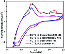
Herein, we report a spin coating route for the deposition of multifunctional quaternary copper chalcogenide Cu2–II–Sn–S4 (II = Fe, Co and Ni) thin films on ITO glass substrates. The surface morphology of the thin films is a uniform porous like structure with an average film thickness of 1.5 μm. The formation of single phase Cu2FeSnS4 (CFTS), Cu2CoSnS4 (CCTS) and Cu2NiSnS4 (CNTS) thin films was confirmed by Raman spectroscopy, which reveals two principal Raman peaks of the A1 phonon mode. Due to the presence of the d6, d7 and d8 electronic configurations within Fe2+, Co2+ and Ni2+ ions, respectively, all the materials show a spin magnetic moment per ion of 3.33 μB, 2.45 μB and 1.31 μB for CFTS, CCTS and CNTS, respectively, as described by the electronic band structure calculation (WIEN2k code). All the thin films have estimated band gap values of 1.87 eV, 1.57 eV and 1.74 eV, respectively, with enhanced photocurrent properties and electrocatalytic activity. Significantly improved charge transfer properties of the thin films were observed from electrochemical impedance spectroscopy analysis under dark and visible light illumination conditions. These thin films are promising for use in photoelectrochemical and solar cell applications.
1. Introduction
In the current thin-film photovoltaic technology, the earth abundant, environmental friendly, low cost, non-toxic quaternary copper based chalcogenides have gained valuable attention as promising light absorbing materials. Recently, Cu2XSnS4 (X = Zn, Fe, Co, Ni) compounds1–6 have been considered ideal light absorbing materials for photovoltaic applications due to their suitable direct band gaps and high light absorption capacity and also they contain earth-abundant elements which are environmentally friendly compared to the traditional solar absorber materials CdTe and CuInGaSe2. There are several synthetic techniques and reports available in the literature on the preparation of CZTS thin films, analysis of their structural and optical properties, theoretical investigation of their electronic band structure (WIEN2k, CASTEM, VASP code, etc.) and also CZTS based solar cell devices,1,3–8 however there are very few reports on other chalcogenides, such as Cu2FeSnS4 (CFTS), Cu2CoSnS4 (CCTS), and Cu2NiSnS4 (CNTS), in the form of a thin film.9–11 However, the wurtzite, stannite or kesterite structure of Cu2FeSnS4 (CFTS), Cu2CoSnS4 (CCTS), and Cu2NiSnS4 (CNTS) compounds, mostly in the form of nanocrystals, has been reported previously.9,10,12–15 Zhang et al. (2012) reported the phase controlled synthesis of wurtzite CFTS nanoparticles with a band gap of 1.50 eV.12 Wang et al. (2014) fabricated Cu2FeSnS4 nanocrystals by ultrasound-assisted microwave irradiation.13 Sarkar et al. (2015) reported the optical and thermo-electric properties of Cu2NiSnS4 nanoparticles synthesized by using a novel hydrothermal route.14 Flower-like Cu2NiSnS4 (CNTS) nanoparticles using a facile solvothermal method were synthesized by T. X. Wang et al. (2014) and they found strong light absorption in the visible light region with a band gap of 1.41 eV.15 X. Zhang et al. (2013) reported wurtzite phased Cu2CoSnS4 nanocrystals by the hot injection method and their photoresponse behaviour was analyzed via the I–V characteristics of thin films of CCTS prepared from the nanocrystals.10 Recently, C. L. Yang et al. (2016) described the structural, optical and magnetic properties of CNTS thin films using a facile one-step electro-deposition method.9 On the other hand, only a few reports have explained the density of states (DOS) and optical bandgaps of CFTS, CCTS and CNTS theoretically.16 Furthermore, reports of the comparative study of the electronic band structure calculation and fundamental properties of CFTS, CCTS and CNTS thin films are lacking. A detailed investigation of the structural stability and density of states of Cu2XSnY4 (X = Fe, Co, Ni; Y = S, Se) has been reported previously via the WIEN2k code17 under generalized gradient approximation (GGA) within the Perdew–Burke–Ernzerhof (PBE)18 parameterization, however the calculated band gap was much smaller than the reported experimental results.12–15
In the present study, we report a simple spin-coating route for the deposition of Cu2FeSnS4 (CFTS), Cu2CoSnS4 (CCTS), and Cu2NiSnS4 (CNTS) thin films. The simple spin-coating deposition technique is attractive due to its low cost and easy control of doping and stoichiometry. This technique has been used vastly to deposit Cu2ZnSn(S and Se)4 thin films and CZTS based thin film solar cells.19–25 However, CFTS, CCTS and CNTS thin films are mostly deposited by electrodeposition,9 electrospinning and spray pyrolysis.10,11 Also, reports on the optical and electrical properties, which are necessary for practical photovoltaic application, and fundamental properties, such as the electronic properties of these thin films, are still lacking. Herein, we analyze the optical and electrical properties of these thin films to show their suitability in photovoltaic application. Moreover, total energy calculations are studied using density functional theory and the more accurate Tran–Blaha modified Becke–Johnson potential26 implemented in the WIEN2k code in order to obtain a comparative study of the electronic band structure, DOS and optical band gap of kesterite phase CFTS, CCTS and CNTS thin films.
2. Experimental
Cu2FeSnS4 thin films were deposited by the spin coating technique starting with a non-aqueous solution. This non aqueous solution was prepared by dissolving copper chloride dihydrate (2 M), iron chloride tetrahydrate (1 M), tin chloride dihydrate (1 M) and thiourea (12 M) in 2-methoxyethanol and a few drops of monoethanolamine (MEA). MEA was used here as a stabilizer. Excess thiourea was used to compensate for sulfur loss during annealing. A clear, brown sol–gel was formed after stirring at 50 °C for several minutes. The resulting solution was deposited onto ITO coated glass substrates by spin coating with a rotation speed of 1400 rpm for 30 s. After the first coating, the substrate was preheated at 150 °C for 10 min to evaporate the solvents and the coating process was repeated five times to obtain the required thickness of the films. Finally, the dense CFTS film was annealed at 300 °C for 20 min.
To enhance this work and to increase the general applicability of this thin film deposition technique, the reaction was repeated with cobalt chloride hexahydrate and nickel chloride hexahydrate precursors, separately, instead of zinc chloride dihydrate. Keeping all other parameters the same, CCTS and CNTS could be formed. These resulting solutions were coated on a ITO substrate in the same process to obtain CCTS and CNTS thin films.
The surface morphologies of the as grown films were observed using a ZEISS Supra 55 field emission scanning electron microscope (FESEM). The crystal phase and structural properties of the grown films were investigated on a Bruker D8 Advance X-ray diffractometer (XRD) using monochromatic Cu-Kα radiation. Additional characterization was done by recording room temperature Raman spectra using a Horiba Jobin Yvon HR800 Raman spectrometer (excitation wavelength 785 nm). The absorbance spectra and optical band gap of the sample were characterized using an Agilent Cary 5000 UV-Vis-NIR double beam spectrophotometer. The photo-responsive behaviour of the as-prepared film was determined by its current–voltage characteristics under dark and light illumination conditions. A KEITHLEY 2450 source model and a solar simulator with the light illumination intensity of one Sun (AM 1.5, 1 kW m−2, NCPRE IIT) were used as the electrical analysis system. Electrochemical measurements were performed on a CHI660C electrochemistry workstation at the Department of Applied Chemistry, Indian Institute of Technology (Indian School of Mines), Dhanbad. A three-electrode system was adopted, in which Ag/AgCl in saturated KCl (0.197 V versus normal hydrogen electrode, NHE) and a Pt electrode were used as the reference and counter electrodes, respectively. The electrolyte was a solution of 0.1 M NaOH solution. In addition, ITO/ZnO nanorods (NR) (preparation and characterization of ZnO NR is given in the ESI†) were also used in place of the Pt electrode and the measurement was carried out in the same system.
3. Computational details
In addition to the above experiments, total energy calculations (WIEN2k code)17 were carried out to study the band structure, density of states and optical property (absorption coefficient) of the as-prepared copper chalcogenide thin films. The WIEN2k code is based on the full potential linear augmented plane wave (FP-LAPW) method of density functional theory. Also, the Tran–Blaha modified Becke–Johnson potential (TB-mBJ)26,27 has been proven to yield much more accurate gaps for numerous semiconductors and insulators28,29 and also to improve the half-metallic gaps for half-metallic materials.26 To optimize the structure, we used an energy cutoff parameter R × Kmax = 7, where R is the average radius of the muffin-tin (MT) spheres, and Kmax is the cutoff for the wave function basis. In addition, the cutoff energy was set to −6 Ry to separate the core state from the valence states. Inside the MT spheres, the angular momentum expansion was expanded up to lmax equal to 10 and it was kept constant throughout the calculation. Due to the effect of the on-site Coulomb repulsion of the 3d electrons of Fe, Co and Ni, the exchange–correlation potential was treated by the GGA + U (U = 5.5 eV) approach used by Dudarev et al.29 We checked with several U-values and their implication on the volume of the cell of U = 5.5 eV provides a significant description of the band gap and also a better lattice constant compared to our experimental as well as the reported values. The detailed parameterizations of the calculation were followed as mentioned in detail previously.4
4. Results and discussion
4.1 Structural properties and surface morphology
The crystalline structures of the Cu2–II–Sn–S4 (II = Fe, Co, Ni) thin films were characterized via X-ray diffraction (XRD) from 2θ values of 20° to 60°. Fig. 1 shows the XRD patterns of Cu2–II–Sn–S4 (II = Fe, Co, Ni) sulfurized at 300 °C for 20 min. The XRD patterns of all the thin films well match with the kesterite structure of CZTS (JCPDS 26-0575).30 No impurity phases of CuS, Cu2S, ZnS are observed in all the samples. To calculate the lattice parameters values of the CFTS, CCTS and CNTS thin films we fitted the main intense peaks (1 1 2), (2 0 0) and (2 2 0) using the XRDA 3.1 software and the calculated values are a = 5.285 Å, 5.281 Å and 5.288 Å for the CFTS, CCTS and CNTS structures, respectively, which are quite similar to the previously reported experimental values (i.e., 5.432 Å for CZTS; 5.4423 Å for CFTS and 5.480 Å for CNTS).5,9,10 The c/a parameter was found to be close the theoretical value of 2 for the ideal tetragonal structure. The c/a values are 2.072, 2.069 and 2.10 for CFTS, CCTS and CNTS respectively. Since the deposition was performed at a low temperature, to examine the presence of impure phases in the CFTS, CCTS and CNTS films, Raman scattering spectra were recorded at the excitation wavelength of 785 nm, which are shown in Fig. 2. The room temperature Raman spectra display the strongest peak at 331.58 cm−1 (for CFTS), 325 cm−1 (for CCTS) and 330.63 cm−1 (for CNTS). These peaks represent the A1 symmetric vibrational motion of sulfur atoms in the CFTS, CCTS and CNTS thin films.2,11,31 Additionally, the second most intense Raman peaks at 284.9 cm−1 (for CFTS), 289 cm−1 (for CCTS) and 284 cm−1 (for CNTS) are also assigned to the kesterite structure of the respective thin films.31,32
 |
| Fig. 1 XRD patterns of the kesterite phase of the Cu2–II–Sn–S4 (II = Fe, Co and Ni) thin films. | |
 |
| Fig. 2 Raman spectra of the Cu2–II–Sn–S4 (II = Fe, Co and Ni) thin films: (a) CFTS, (b) CCTS and (c) CNTS. | |
Fig. 3 shows the FESEM surface morphology of the CFTS, CCTS and CNTS thin films annealed at the temperature of 300 °C. It has been found that all the films are compact and uniformly grained. This porous like morphology is useful as an absorber layer for device fabrication. The average elemental composition of the deposited thin films was determined by energy-dispersive X-ray spectroscopy (EDX), which confirmed in the desired 2
:
1
:
1
:
4 ratio (shown in Fig. S1†).
 |
| Fig. 3 FESEM images of the Cu2–II–Sn–S4 (II = Fe, Co and Ni) thin films: (a) CFTS, (b) CCTS and (c) CNTS. | |
4.2 Electrical properties
4.2.1 Photocurrent measurement. The photoresponse behaviour of the as-synthesized Cu2–II–Sn–S4 (II = Fe, Co, Ni) thin films was studied in order to evaluate their potential as an active layer for photovoltaic applications. The current–voltage (I–V) characteristics of the Cu2–II–Sn–S4 (II = Fe, Co and Ni) thin films are shown in Fig. 4. These I–V curves were measured both in the dark and under illumination using a solar simulator (AM 1.5 irradiation, 100 mW cm−2) at room temperature in the range of −4 V to +4 V. All the samples show ohmic behaviour and a current enhancement is observed under illumination, as shown in Fig. 4, which is quite similar with the previously reported semiconductor nanocrystal films.6,10,33 From this figure, it is clear that the enhancement of current for CCTS is much more compared to the CFTS and CNTS thin films. This is may be due to the optimum band gap values of the CCTS thin films.34,35
 |
| Fig. 4 Photocurrent measurements under dark and 1.5 AM light illumination at room temperature for the CFTS, CCTS and CNTS thin films. | |
4.2.2 Cyclic voltammetry (CV) analysis. To investigate the electro catalytic activity of the CFTS, CCTS and CNTS thin film electrodes, cyclic voltammetry (CV) was carried out in a three electrode system with 0.1 M NaOH electrolyte solution in the potential range of −1.5 V to +0.5 V at different scan rates (ν = 5, 25, 50 & 100 mV s−1) with respect to the Ag/AgCl reference electrode. Here, both platinum and ZnO nanorod electrodes were used as the counter electrode to compare the electrocatalytic response of the thin film electrodes. Fig. 5 shows the cyclic voltammogram curves of the thin film electrodes with obvious cathodic peaks under dark and visible light illumination using the Pt cathode electrode. The cyclic voltammogram curves of the thin film electrodes under dark and visible light illumination in the presence of the ZnO NR counter electrode are shown in Fig. S2 (ESI†). An increase in the scan rate increased the area under the curve, which gives the cathodic peaks maximum current density. From Fig. 5, it can also be evaluated that the maximum cathodic current densities for CFTS, CCTS and CNTS were 6.13 mA cm−2, 4.92 mA cm−2 and 7.14 mA cm−2 at the potential of −0.331 V, −0.473 V and −0.454 V, respectively, (at a scan rate of 100 mV s−1 and Pt counter electrode). The cathodic peak current density for CNTS is observed to be higher than that of CFTS and CCTS. These copper chalcogenide thin films can be used as electrode materials for solar cells and photo electrochemical cells.2,36 Our calculated cathodic peak current density values for CFTS and CCTS are higher than that previously reported by Mokurala et al.37 According to the literature, the better performance of electrocatalytic activity depends on the specific surface area, morphology and elemental composition of quaternary chalcopyrite sulphides.35,38 The higher cathodic peak current density value of the CCTS film from the previous report might be due to the higher specific surface area and the maintenance of the stoichiometric composition of CCTS and also its band gap values.35,38 The increased anodic and cathodic current under visible light illumination reveals increased capacitance behaviour.2,36 In addition, the enhanced capacitive performance of the CFTS, CCTS and CNTS photo electrodes with respect to the ZnO nanorod cathode electrode can be given as an alternative and better performance in the charge storing system under visible light irradiation.
 |
| Fig. 5 (a–c) Cyclic voltammograms of CFTS, CCTS and CNTS, respectively, at a sweep rate of ν = 5, 25, 50 and 100 mV s−1 under dark (D) and visible light (L) illumination using a Pt electrode as the cathode electrode. The insets show the variation of CV of all respective thin films (at a sweep rate of 5 mV s−1) with respect to Pt and ZnO cathode electrodes under dark (D) and visible light (L) illumination. | |
In addition, electrochemical impedance spectroscopy (EIS) analysis was performed under dark and visible light illumination over the frequency range of 100 kHz to 10 mHz with an amplitude of 5 mV. Fig. 6 shows the Nyquist plot for the CFTS, CCTS and CNTS electrodes with respect to the platinum (Pt) (Fig. 6a) and ZnO NR (Fig. 6b) counter electrode under dark and visible light illumination. On the basis of the equivalent circuit described in the literature, our measured impedance curves in the Nyquist plot can be well-fitted with an equivalent circuit, which consists of a resistance (Rs), charge transfer resistance (Rct), solid electrolyte interface resistance (SEI) resistance (Rf) and constant phase element (Q). The resistance Rs is correlated to the internal resistance, which includes the inbuilt electrode resistances, the electrolyte and the contact resistance grown between the electrode and current collector. The charge transfer resistance, Rct, is inversely proportional to charge recombination. Rf represents resistances due to the specific area, morphology and crystallinity of the working electrode.39–41 The impedance parameters were analyzed from least-squares fit to an equivalent circuit using the ZSimpWin 3.22d software. The fitted parameters of Rs, Rct and Rf from the Nyquist plots are summarized in Table 1. The EIS Nyquist plots for all the thin films under dark and visible light irradiation indicate good charge transfer between solid electrolyte interfaces. According to the EIS data, it is clear that the resistance of all the thin film electrodes (CFTS, CCTS and CNTS) decreases under visible light illumination conditions. The use of ZnO NR as a counter electrode improves the charge transfer capacity between the solid electrolyte interfaces. Generally, a smaller value of Rct represents a higher electro-catalytic activity towards the redox electrolyte. Swami et al.35 described that films of CZTS, which have lower Rct values, show good catalytic activity. Here, from Table 1, we can see that the value of Rct both under dark and illumination conditions is reduced when the counter electrode is replaced by ITO/ZnO nanorods. Therefore, it is obvious that catalytic activity of the thin films is improved by replacing the platinum counter electrode. This improvement in charge transport is attributed to the enhancement in interface area (via ZnO nanorods) and the work function difference of platinum and ZnO. Thus, our experimental results provide strong evidence that ZnO nanorods could be use as an alternative to the platinum counter electrode for improvement in the photo electrochemical response of the individual thin films.
 |
| Fig. 6 Nyquist plots of the CFTS, CCTS and CNTS thin films with different cathode electrodes under dark and visible light illumination conditions: (a) cathode electrode: Pt electrode, and (b) cathode electrode: ZnO NR. Inset represents the equivalent circuit of the thin films. | |
Table 1 Impedance parameter results obtained from the equivalent circuit for the CFTS, CCTS and CNTS samples with respect to the platinum and ITO/ZnO counter electrode
Sample |
Counter electrode |
Rs (Ω) |
Rct (Ω) |
Rf (Ω) |
Total resistance (Ω) TR = Rs + Rct + Rf |
CFTS (dark) |
Platinum |
1.148 |
6828 |
622.2 |
7451.34 |
CFTS (illumination) |
1 |
1377 |
279.2 |
1657.2 |
CCTS (dark) |
Platinum |
1.065 |
4016 |
5.268 |
4022.33 |
CCTS (illumination) |
0.01 |
1409 |
2.415 |
1411.42 |
CNTS (dark) |
Platinum |
1.123 |
3138 |
23.67 |
3162.79 |
CNTS (illumination) |
1 |
1821 |
7.538 |
1829.53 |
CFTS (dark) |
ITO/ZnO nanorods |
100 |
1744 |
194.4 |
2038.40 |
CFTS (illumination) |
0.01 |
1037 |
134.7 |
1171.71 |
CCTS (dark) |
ITO/ZnO nanorods |
0.01 |
2617 |
929.4 |
2946.41 |
CCTS (illumination) |
0.01 |
430 |
217.8 |
647.81 |
CNTS (dark) |
ITO/ZnO nanorods |
0.01 |
3187 |
29.4 |
3216.41 |
CNTS (illumination) |
100 |
1228 |
18.53 |
1346.53 |
4.3 Electronic property
4.3.1 Band structure. The calculated band structures of Cu2–II–Sn–S4 (II = Fe, Co and Ni) are shown in Fig. 7. All the compounds show similar band structures and band gaps in the majority states occurring at the Fermi energy EF. This majority gap is characteristic of half-metallic materials, as was previously shown by various authors.16,26,29 The main contributions in the band structure and the total density of states are due to the Cu: 4s, 3p, 3d, Fe: 3d, 4s, Co: 3d, 4s, Ni: 3d, 4s, Sn: 4d, 5s, 5p, and S: 3s, 3p states. Here, Fe2+, Co2+ and Ni2+ have the d6, d7 and d8 electronic configurations, respectively. Therefore, for the majority spin case the primary component of the conduction band, e.g. 3d-bands, are not fully occupied and for down spin it remains empty. As a result, an occupied 3d band in a spin up is mixed with anion-3p bands and shows the semiconductor behavior. On the other hand, the minority spin shows a metallic nature. The contribution of all valance states in the majority and minority spin band structure is shown in the ESI.† The total and partial density of states (DOS) for all the compounds are shown in Fig. S3–S5.† From the DOS plots, it found that the valence band regions are mainly comprised of bonding states from −5 eV to −0.15 eV, which consist of S-p states hybridized with the Cu-3d state. On the other conduction band side near the Fermi energy (EF), Sn-p has the highest contribution. Thus, this p–d hybridization mainly opens the band gap in the majority spin states. The magnetic spin configuration of the Fe-3d (d5), Co-3d (d7) and Ni-3d (d8) states shows the spin magnetic moment per ion of 3.33 μB, 2.45 μB and 1.31 μB for CFTS, CCTS and CNTS, respectively, which is good agreement with the previously reported results.16
 |
| Fig. 7 Spin-resolved electronic band structure of Cu2FeSnS4 (CFTS), Cu2CoSnS4 (CCTS) and Cu2NiSnS4 (CNTS): (a–c) majority and (d–f) minority electrons, respectively. | |
4.4 Optical property
The optical absorption properties of the films were investigated by UV-Vis spectroscopy. Fig. 8 presents the absorbance spectra of the CFTS, CCTS and CNTS thin films in the wavelength range of 350 to 1200 nm. We can find from this figure that all the thin films have high optical absorption values with respect to the photon energy of solar irradiation. To determine the band gap of the as-deposited thin films we plotted (Ahν)2 versus hν (A = absorbance; h = Planck's constant and ν = frequency) and then extrapolated the linear portion of the spectrum in the band edge region. Fig. 8b–d show the Tauc plots of all the thin films. The band gaps (experimental) of these materials are found to be 1.87 eV, 1.57 eV and 1.74 eV for the CFTS, CCTS and CNTS thin films, respectively, which are in agreement with the band gap values reported for CFTS, CCTS and CNTS thin films by other authors.9–11 The estimated band gap values from the WIEN2k calculation are 1.67 eV, 1.57 eV and 1.52 eV for CFTS, CCTS and CNTS, respectively. It has been observed that our calculated experimental band gap values and simulated band gap values (WIEN2k calculated) are quite similar. The improvement in the theoretical estimated band gap values occurs due to the use of the TB-mBJ potential.
 |
| Fig. 8 (a) Absorption spectra, (b–d) Tauc plots of the CFTS, CCTS and CNTS thin films (experimental), and (e) Tauc plots of CFTS, CCTS and CNTS through simulation: WIEN2k code. | |
5. Conclusions
In summary, thin films of Cu2FeSnS4, Cu2CoSnS4 and Cu2NiSnS4 have been deposited successfully on ITO substrates by a simple sol–gel and spin-coating technique. The kesterite structures of the films result from the synthetic process at a temperature of over 250 °C. The formation of a homogeneous, uniformly grained and dense surface morphology was observed via FESEM. The optical band gap values (1.57–1.87 eV) of all the materials are ideal for low cost, thin film inorganic solar cells. The electronic band structure calculation (FP-LAPW method) describes the half metallic behavior and the films as being semiconductors with majority spin channel and metals with the spin minority channel. The present study of the TB-mBJ potential within the FP-LAPW method provides a better description of the improvement of band gap from previous reported theoretical results. The photoresponse behaviour was observed in the I–V characteristics of thin films. Cyclic voltammetry (CV) measurements show the higher electrocatalytic activity of the CCTS thin film electrode compared to the CFTS and CNTS film electrodes. Also, electrochemical impedance spectroscopy (EIS) analysis reveals the reduction of resistance under visible light illumination and it proves that the use of ZnO NRs as a counter electrode improves the charge transfer capacity between solid electrolyte interfaces. The present easy synthetic method, photoactivity and electrocatalytic activity of the thin films can likely be extended to the synthesis of a wide range of quaternary chalcogenide semiconductors for nano- and microstructured photoelectric devices.
Acknowledgements
The authors acknowledge for the financial support from the Indian Institute of Technology (Indian School of Mines), Dhanbad, India, Central Research Facility (CRF) and Department of Science and Technology (DST) for project with grant number SR/FTP/PS-184/2012, SERB video y.No.SERB/F/5439/2013-14 dated 25.11.2013 and Faculty Research Scheme FRS (54)/2013-2014/APH.
References
- H. Katagiri, N. Sasaguchi, S. Hando, S. Hoshino, J. Ohashi and T. Yokota, Preparation and evaluation of Cu2ZnSnS4 thin films by sulfurization of EB evaporated precursors, Sol. Energy Mater. Sol. Cells, 1997, 49, 407–414 CrossRef CAS.
- K. Mokurala, S. Mallick and P. Bhargava, Alternative quaternary chalcopyrite sulfides (Cu2FeSnS4 and Cu2CoSnS4) as electrocatalyst materials for counter electrodes in dyesensitized solar cells, J. Power Sources, 2016, 305, 134–143 CrossRef CAS.
- K. Tanaka, M. Kurokawa, K. Moriya and H. Uchiki, Surface morphology improvement of three-dimensional solar cell with Cu2ZnSnS4 absorber, J. Alloys Compd., 2013, 571, 98–102 CrossRef CAS.
- A. Ghosh, R. Thangavel and M. Rajagopalan, First principles study of electronic and optical properties of Cu2ZnSnX4 (X = S, Se) solar absorbers by Tran–Blaha-modified Beckee Johnson potential approach, J. Mater. Sci., 2013, 48, 8259–8267 CrossRef CAS.
- B. J. Li, P. F. Yin, Y. Z. Zhou, Z. M. Gao, T. Ling and X. W. Du, Single crystalline Cu2ZnSnS4 nanosheet arrays for efficient photochemical hydrogen generation, RSC Adv., 2015, 5, 2543–2549 RSC.
- Y. Cui, R. Deng, G. Wang and D. Pan, A general strategy for synthesis of quaternary semiconductor Cu2MSnS4 (M = Co2+, Fe2+, Ni2+, Mn2+) nanocrystals, J. Mater. Chem., 2012, 22, 23136–23140 RSC.
- C. Persson, Electronic and optical properties of Cu2ZnSnS4 and Cu2ZnSnSe4, J. Appl. Phys., 2010, 107, 053710–053718 CrossRef.
- S. S. Mali, P. S. Patil and C. K. Hong, Low-cost electrospun highly crystalline kesterite Cu2ZnSnS4 nanofiber counter electrodes for efficient dye-sensitized solar cells, ACS Appl. Mater. Interfaces, 2014, 6, 1688–1696 CAS.
- C. L. Yang, Y. H. Chen, M. Lin, S. L. Wu, L. Li, W. C. Liu, X. S. Wu and F. M. Zhang, Structural, optical and magnetic properties of Cu2NiSnS4 thin films deposited by facile one-step electro deposition, Mater. Lett., 2016, 166, 101–104 CrossRef CAS.
- X. Zhang, N. Bao, B. Lin and A. Gupta, Colloidal synthesis of wurtzite Cu2CoSnS4 nanocrystals and the photoresponse of spray-deposited thin films, Nanotechnology, 2013, 24, 105706–105708 CrossRef PubMed.
- D. B. Khadka and J. H. Kim, Structural, optical and electrical properties of Cu2FeSnX4 (X = S, Se) thin films prepared by chemical spray pyrolysis, J. Alloys Compd., 2015, 638, 103–108 CrossRef CAS.
- X. Zhang, N. Bao, K. Ramasamy, Y. H. A. Wang, Y. Wang, B. Lin and A. Gupta, Crystal phase-controlled synthesis of Cu2FeSnS4 nanocrystals with a band gap of around 1.5 eV, Chem. Commun., 2012, 48, 4956–4958 RSC.
- W. Wang, H. Shen, H. Yao and J. Li, Preparation and properties of Cu2FeSnS4 nanocrystals by ultrasound-assisted microwave irradiation, Mater. Lett., 2014, 125, 183–186 CrossRef CAS.
- S. Sarkar, B. Das, P. R. Midya, G. C. Das and K. K. Chattopadhyay, Optical and thermoelectric properties of chalcogenide based Cu2NiSnS4 nanoparticles synthesized by a novel hydrothermal route, Mater. Lett., 2015, 152, 155–158 CrossRef CAS.
- T. X. Wang, Y. G. Li, H. R. Liu, H. Li and S. X. Chen, Flower-like Cu2NiSnS4 nanoparticles synthesized by a facile solvothermal method, Mater. Lett., 2014, 124, 148–150 CrossRef CAS.
- A. Ghosh, R. Thangavel and M. Rajagopalan, First-Principles Study of Structural Stability and Optical Properties of Cu2XSnY4 (X = Fe, Co, Ni; Y = S, Se) for Photovoltaic Applications, Energy Environ. Focus, 2014, 3, 142–151 CrossRef.
- P. Blaha, K. Schwarz, G. K. H. Madsen, D. Kvasnicka and J. Luitz, WIEN2k an Augmented Plane
Wave + Local Orbitals Program for Calculating Crystal Properties, ed. K. Schwarz, Techn, University at Wien, Austria, 2001, ISBN 3-501031-1-2 Search PubMed.
- J. P. Perdew, K. Burke and M. Ernzerhof, Stabilization of Long-Range Magnetic Order in 2D Easy-Plane Antiferromagnets, Phys. Rev. Lett., 1996, 77, 386–395 CrossRef PubMed.
- D. Lee and K. Yong, Solution-processed Cu2ZnSnS4 superstrate solar cell using vertically aligned ZnO nanorods, Nanotechnology, 2014, 25, 065401–065408 CrossRef PubMed.
- S. K. Swami, A. Kumar and V. Dutta, Deposition of Cu2ZnSnS4 (CZTS) thin films by spin coating technique for solar cell application, Energy Procedia, 2013, 33, 198–202 CrossRef CAS.
- K. D. Zhang, Z. R. Tian, J. B. Wang, B. Li, X. L. Zhong, D. Y. Guo and S. M. He, Preparation of Cu2ZnSnS4 thin films using spin-coating method with thermolysis and annealing, J. Sol-Gel Sci. Technol., 2015, 73, 452–459 CrossRef CAS.
- G. M. Ilari, C. M. Fella, C. Ziegler, A. R. Uhl, Y. E. Romanyuk and A. N. Tiwari, CuZn2SnSe4 solar cell absorbers spin coated from amine containing ether solutions, Sol. Energy Mater. Sol. Cells, 2012, 104, 125–130 CrossRef CAS.
- H. Park, Y. H. Hwang and B.-S. Bae, Sol gel processed Cu2ZnSnS4 thin films for a photovoltaic absorber layer without sulfurization, J. Sol-Gel Sci. Technol., 2013, 65, 23–27 CrossRef CAS.
- K. Tanaka, M. Oonuki, N. Moritake and H. Uchiki, Cu2ZnSnS4 thin film solar cells prepared by non-vacuum processing, Sol. Energy Mater. Sol. Cells, 2009, 93, 583–587 CrossRef CAS.
- F. Yakuphanoglu, Nanostructure Cu2ZnSnS4 thin film prepared by sol–gel for optoelectronic applications, Solar Energy, 2011, 85, 2518–2523 CrossRef CAS.
- F. Tran and P. Blaha, Accurate Band Gaps of Semiconductors and Insulators with a Semilocal Exchange–Correlation Potential, Phys. Rev. Lett., 2009, 102, 226401 CrossRef PubMed.
- K. David, F. Tran and P. Blaha, Improving the modified Becke–Johnson exchange potential, Phys. Rev. B: Condens. Matter Mater. Phys., 2012, 85, 155109 CrossRef.
- C. Shiyou, X. G. Gong, W. Aron and S.-H. Wei, Crystal and electronic band structure of Cu2ZnSnX4 (X = S and Se) photovoltaic absorbers: first-principles insights, Appl. Phys. Lett., 2009, 94, 041903 CrossRef.
- S. L. Dudarev, G. A. Botton, S. Y. Savrasov, C. J. Humphreys and A. P. Sutton, Electron-energy-loss spectra and the structural stability of nickel oxide: an LSDA+U study, Phys. Rev. B: Condens. Matter Mater. Phys., 1998, 57, 1505–1509 CrossRef CAS.
- B. Shin, O. Gunawan, Y. Zhu, N. A. Bojarczuk, S. J. Chey and S. Guha, Thin film solar cell with 8.4% power conversion efficiency using an earth-abundant Cu2ZnSnS4 absorber, Prog. Photovoltaics Res. Appl., 2013, 21, 72–76 CrossRef CAS.
- O. P. Singh, K. S. Gour, R. Parmar and V. N. Singh, Sodium induced grain growth, defect passivation and enhancement in the photovoltaic properties of Cu2ZnSnS4 thin film solar cell, Mater. Chem. Phys., 2016, 177, 293–298 CrossRef CAS.
- X. Fontane, V. Izquierdo-Roca, E. Saucedo, S. Schorr, V. O. Yukhymchuk, M. Y. Valakh, A. Perez-Rodriguez and J. R. Morante, Vibrational properties of stannite and kesterite type compounds: Raman scattering analysis of Cu2(Fe,Zn)SnS4, J. Alloys Compd., 2012, 539, 190–194 CrossRef CAS.
- X. Lu, Z. Zhuang, Q. Peng and Y. Li, Wurtzite Cu2ZnSnS4 nanocrystals: a novel quaternary semiconductor, Chem. Commun., 2011, 47, 3141–3143 RSC.
- B. Murali, M. Madhuri and S. B. Krupanidhi, Solution Processed Cu2CoSnS4 Thin Films for Photovoltaic Applications, Cryst. Growth Des., 2014, 14, 3685–3691 CAS.
- S. K. Swami, N. Chaturvedi, A. Kumar, N. Chander, V. Dutta, D. K. Kumar, A. Ivaturi, S. Senthilarasu and H. M. Upadhyaya, Spray deposited copper zinc tin sulphide (Cu2ZnSnS4) film as a counter electrode in dye sensitized solar cells, Phys. Chem. Chem. Phys., 2014, 16, 23993–23999 RSC.
- J. Y. Park, J. H. Noh, T. N. Mandal, S. H. Im, Y. Jun and S. Il Seok, Quaternary semiconductor Cu2FeSnS4 nanoparticles as an alternative to Pt catalysts, RSC Adv., 2013, 3, 24918–24921 RSC.
- K. Mokurala, S. Mallick and P. Bhargava, Alternative quaternary chalcopyrite sulfides (Cu2FeSnS4 and Cu2CoSnS4) as electrocatalyst materials for counter electrodes in dye sensitized solar cells, J. Power Sources, 2016, 305, 134–143 CrossRef CAS.
- M. S. Fan, J. H. Chen, C. T. Li, K. W. Cheng and K. C. Ho, Copper zinc tin sulfide as a catalytic material for counter electrodes in dye-sensitized solar cells, J. Mater. Chem. A, 2015, 3, 562–569 CAS.
- P. A. Fernandes, A. F. Sartori, P. M. P. Salome, J. Malaquias, A. F. da Cunha, M. P. F. Grac and J. C. Gonzalez, Admittance spectroscopy of Cu2ZnSnS4 based thin film solar cells, Appl. Phys. Lett., 2012, 100, 233504 CrossRef.
- Y. Hou, H. Azimi, N. Gasparini, M. Salvador, W. Chen, L. S. Khanzada, M. Brandl, R. Hock and C. J. Brabec, Low-Temperature Solution-Processed Kesterite Solar Cell Based on in Situ Deposition of Ultrathin Absorber Layer, ACS Appl. Mater. Interfaces, 2015, 7, 21100–21106 CAS.
- E. Kask, J. Krustok, S. Giraldo, M. Neuschitzer, S. Lopez-Marino and E. Saucedo, Temperature dependent electrical characterization of thin film Cu2ZnSnSe4 solar cells, J. Phys. D: Appl. Phys., 2016, 49, 085101–085106 CrossRef.
Footnote |
† Electronic supplementary information (ESI) available. See DOI: 10.1039/c6ra15700a |
|
This journal is © The Royal Society of Chemistry 2016 |
Click here to see how this site uses Cookies. View our privacy policy here.