DOI:
10.1039/C6RA15210D
(Paper)
RSC Adv., 2016,
6, 79952-79957
Efficient inverted planar formamidinium lead iodide perovskite solar cells via a post improved perovskite layer
Received
12th June 2016
, Accepted 31st July 2016
First published on 1st August 2016
Abstract
Formamidinium lead iodide (FAPbI3) is a more promising broader absorption material than methylammonium lead iodide (MAPbI3) for perovskite solar cells (PSCs). However, in most cases the power conversion efficiencies (PCE) of FAPbI3 based inverted planar PSCs are still lower than those of MAPbI3 ones due to the inferior morphology of FAPbI3 film. In this paper, we demonstrate an optimised formamidinium iodide/isopropyl alcohol (FAI/IPA) modification procedure to improve the photoactive layer for efficient inverted planar FAPbI3 PSCs. The results show that there is an obvious improvement in open circuit voltage, short current density (JSC), and fill factor (FF). Finally, the best PCE of 14.00% with a JSC of 21.75 mA cm−2 and a FF of 0.78 was achieved in low-temperature solution-processed PSCs, which represents a more than 40% enhancement in PCE over that of the PSCs without surface modification. Moreover, the devices exhibit good reproducibility and excellent stability. The simple FAI/IPA modification on the photoactive layer can greatly improve planar FAPbI3 based device performance, which can be a good choice for practical applications.
1. Introduction
Since the first attempt of dye-sensitized solar cells employing inorganic–organic hybrid perovskite as a photoactive layer (with a power conversion efficiency (PCE) of 3.8%)1 was reported, remarkable progress has been made in organometal halide perovskite (methylammonium lead triiodide: MAPbI3 and formamidinium lead triiodide: FAPbI3) based solar cells, including in interface materials,2,3 structure engineering,4–7 perovskite film processing methodologies,8–13 and so on. As a result, PCEs of over 20% have been achieved.14–16 Recently, FAPbI3 based solar cells have drawn much attention for their outstanding performance. The bandgap of FAPbI3 was estimated to be 1.50 eV, smaller than that of MAPbI3 (1.55 eV),17 which has broader absorption of the solar spectrum.18,19 In addition, another advantage is that no significant phase transition occurs at operating temperature.20 As far as commercialization is concerned, such thermal stability is an exceedingly promising property, which is in favor of better long-term thermal durability, and will be one of the key subjects for further investigations.
In previous reports, most PSCs employed a normal configuration with mesoporous or planar metal oxide layer, therefore, a high annealing temperature (400–500 °C) is needed, which is not compatible with low cost and flexible devices.21–26 Hence, planar heterojunction devices with an inverted structure were put forward,27–29 based on a transparent conductive oxide (indium tin oxide, ITO), hole transport material poly(3,4-ethylenedioxythiophene):poly(styrenesulfonate): (PEDOT:PSS), organometal halide perovskite photoactive layer, electron transport material ([6,6]-phenyl-C61-butyric acid methyl ester: PCBM) and metal electrode, i.e., ITO/PDOT:PSS/perovskite/PCBM/Al, which is commonly used in MAPbI3 based PSCs. Such configuration enables the fabrication of flexible, wearable devices at low temperature. However, the quality of perovskite film cannot meet the need for high performance planar devices via a simple one step method, as the growth of perovskite film on a smooth surface is more inhomogeneous. Various deposition methodologies, such as vacuum evaporation,6 sequential deposition,8 solvent-engineering,9 vapor-assisted deposition12 and additive-assisted deposition13 have been developed. These film preparation methods have been proved to be more effective in depositing high-quality MAPbI3 films with complete surface coverage but are not effective enough for preparing high-quality pure FAPbI3 films. Therefore, effective methods are needed to improve the quality of FAPbI3 film. In this regard, several efforts have been developed by some teams. Seok et al. report intramolecular exchange fabrication of FAPbI3 films.14 Qi et al. use a chemical vapor deposition (CVD) method to fabricate FAPbI3 based PSCs with reproducibility and tunable chlorine concentration.30 However, these methods are unsuitable for large-area cost-effective practical applications. Here, we demonstrate a formamidinium iodide/isopropyl alcohol (FAI/IPA) modification procedure on the surface photoactive layer to fabricate efficient inverted FAPbI3 based PSCs. The film qualities, including film morphology, thickness and crystallinity, are greatly improved, and the defect density is also effectively suppressed via FAI/IPA modification, which gives rise to an obvious improvement in device performance.
2. Experimental section
2.1. Materials preparation
FAI was synthesized as previously reported.31 Briefly, by reacting formamidine acetate with 2× molar excess of hydroiodic acid (45 wt% in water) in a 250 mL round-bottomed flask at 50 °C for 10 min with stirring. A yellowish raw precipitate was formed after rotary evaporation at 50 °C. The precipitate was washed with diethyl ether and recrystallized twice with a mixed solvent of ethanol and diethyl ether to form white needle-like crystals. Then it was dried at 60 °C in a vacuum oven for 12 h. PEDOT:PSS (Clevious PVP Al4083), PbI2 and PCBM were purchased from H. C. Starck, Aladdin reagent and American Dye Sources, respectively. All of the materials were used as received unless specially emphasized. ITO glass substrates with a sheet resistance of 15 Ω sq−1 were purchased from Shenzhen Display.
2.2. Solar cell fabrication
A concentration of 1.0 M perovskite precursor solution was prepared by dissolving FAI with an equal molar ratio of PbI2 in a mixed solvent of γ-butyrolactone (GBL) and dimethyl sulfoxide (DMSO) (GBL![[thin space (1/6-em)]](https://www.rsc.org/images/entities/char_2009.gif) :DMSO = 7:3), stirring overnight before use. FAI/IPA solution was prepared by dissolving FAI into anhydrous IPA with an optimized concentration of 2 mg mL−1. The ITO coated glass substrates were precleaned sequentially in detergent, deionized water, acetone, and isopropyl alcohol and then treated in oxygen plasma. The PEDOT:PSS (Clevious AI 4083) layer (30 nm) was coated by spin-coating at 4000 rpm for 20 s, and annealed at 150 °C for 20 min in air. The precursor solution was spin coated on the PEDOT:PSS layer using a fast deposition crystallization procedure11 in a nitrogen filled glovebox. The precursor solution was spin-coated at 4000 rpm or 6000 rpm to control its thickness. Then, the FAPbI3 coated substrate was put on a hot plate and annealed at 150 °C for 10 min, the modification procedure of FAPbI3 film was performed by spin coating FAI/IPA solution on the film surface at 4000 rpm. Samples were annealed at 150 °C for 20 min. After cooling down to room temperature, 40 nm thick PCBM (15 mg mL−1 in chlorobenzene) was spin-coated on the perovskite layer. Finally, the films were transferred into a thermal evaporation system for Al cathode evaporation. The active area is 0.1 cm2 defined by the shadow mask. FAPbI3 based solar cells without FAI/IPA modification were also fabricated for comparison.
:DMSO = 7:3), stirring overnight before use. FAI/IPA solution was prepared by dissolving FAI into anhydrous IPA with an optimized concentration of 2 mg mL−1. The ITO coated glass substrates were precleaned sequentially in detergent, deionized water, acetone, and isopropyl alcohol and then treated in oxygen plasma. The PEDOT:PSS (Clevious AI 4083) layer (30 nm) was coated by spin-coating at 4000 rpm for 20 s, and annealed at 150 °C for 20 min in air. The precursor solution was spin coated on the PEDOT:PSS layer using a fast deposition crystallization procedure11 in a nitrogen filled glovebox. The precursor solution was spin-coated at 4000 rpm or 6000 rpm to control its thickness. Then, the FAPbI3 coated substrate was put on a hot plate and annealed at 150 °C for 10 min, the modification procedure of FAPbI3 film was performed by spin coating FAI/IPA solution on the film surface at 4000 rpm. Samples were annealed at 150 °C for 20 min. After cooling down to room temperature, 40 nm thick PCBM (15 mg mL−1 in chlorobenzene) was spin-coated on the perovskite layer. Finally, the films were transferred into a thermal evaporation system for Al cathode evaporation. The active area is 0.1 cm2 defined by the shadow mask. FAPbI3 based solar cells without FAI/IPA modification were also fabricated for comparison.
2.3. Characterizations
Film thicknesses were measured using a Veeco Dektak 150 surface profiler. X-ray diffraction (XRD) patterns were obtained from a Bruker D8 ADVANCE. Ultraviolet-visible spectroscopy (UV-vis) was performed from 450 to 850 nm via Hitachi U-4100. A scanning electron microscope (SEM, Hitachi S-4800) was used for surface morphology characterization. Current density–voltage (J–V) characteristics of the devices were measured in a N2-filled glovebox with a Keithley 2420 source measurement under AM1.5G, 100 mW cm−2 (Newport). The light intensity was calibrated using a standard silicon solar cell. The J–V curves were obtained via reverse scan (from bias 1.2 V to −0.1 V) and the scan rate was 0.1 V s−1. The external quantum efficiency (EQE) of the solar cell was analysed using a certified Newport incident photon conversion efficiency (IPCE) measurement system. Steady-state photoluminescence (PL) spectra were recorded on a Fluoromax 4 spectrometer (HORIBA Jobin Yvon) with a photoexcitation at 680 nm.
3. Results and discussion
3.1. Film properties
Fig. 1 shows the X-ray diffraction patterns of the FAPbI3 films with and without FAI/IPA modification. The FAPbI3 films exhibit highly oriented crystallinity with a strong preferred orientation of (110). The diffraction peaks, with calculated cell parameters of a = b = 8.98 Å and c = 10.99 Å, are in good agreement with the black phase of tetragonal FAPbI3 as previously reported, with cell parameters a = b = 8.99 Å and c = 11.0 Å.32 However, there is a weak PbI2 peak (labeled #) in the film without FAI/IPA modification. The PbI2 peak is eliminated with FAI/IPA modification, which indicates that a much purer crystalline phase is formed. Furthermore, the enhanced (110) peak with respect to (220) and (222) peaks indicates an increased orientation of crystalline domains. The enhanced crystalline film could be beneficial for the improvement of device performance.
 |
| | Fig. 1 XRD patterns of FAPbI3 perovskite films on ITO/PEDOT:PSS substrate. | |
Fig. 2 shows the UV-vis spectra of the FAPbI3 films prepared under different conditions. The detailed preparation conditions and related parameters are given in Table 1. As shown in Fig. 2, the absorption cut-off edges of the films are at about 825 nm, corresponding to a bandgap of 1.50 eV, which is in agreement with the previous report.17 After FAI/IPA surface modification, there is a slight thickness increase in the perovskite layer. With the increased film thickness, the absorption intensity is enhanced. However, there is an abnormal phenomenon, i.e., the absorption intensity of film D (310 nm) is slightly stronger than that of film A (330 nm). As can be seen in Fig. 3b, the film has lots of small grains after FAI/IPA modification, which can increase the light scattering and absorption. The improved morphology of the perovskite films with FAI/IPA modification could lead to an enhancement in device performance and will be discussed below. The cross-sectional SEM view of device B with the structure of glass/ITO/PEDOT:PSS/FAPbI3/PCBM/Al is shown in Fig. 2b. The thickness of FAPbI3 is about 350 nm, which is coincident with the value obtained by surface profile.
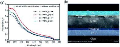 |
| | Fig. 2 UV-vis spectra of FAPbI3 perovskite films prepared under different conditions (a), and cross-sectional SEM view of a completed device (b). | |
Table 1 Device parameters prepared under different conditions
| Device |
Spin speed (rpm) |
Thickness (nm) |
JSC (mA cm−2) |
VOC (V) |
Fill factor |
PCE (%) |
| A (−) |
4k |
330 |
18.83 |
0.79 |
0.71 |
10.58 |
| B (+) |
4k |
350 |
21.75 |
0.82 |
0.78 |
14.00 |
| C (−) |
6k |
290 |
17.66 |
0.81 |
0.64 |
9.19 |
| D (+) |
6k |
310 |
20.17 |
0.86 |
0.72 |
12.59 |
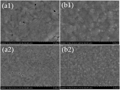 |
| | Fig. 3 SEM images of FAPbI3 perovskite film: (a) without FAI/IPA modification (b) with FAI/IPA modification. | |
Pinholes and cracks of the films are detrimental to device performance. A compact film with full coverage is necessary for high-performance planar PSCs.33 SEM images of the FAPbI3 films with and without FAI/IPA modification with different scale bars are shown in Fig. 3. One can see that the grain size of the perovskite film is about 200–500 nm. Pinholes and cracks are obviously observed in Fig. 3a, which may be ascribed to the strain and vaporization of the residual solvent during thermal annealing. The cracks and pinholes tend to increase the area of direct contact between the anode and cathode, which could lead to poor device performance. After surface modification with FAI/IPA, lots of smaller secondary grains were formed as shown in Fig. 3b, which results in a more compact high-quality perovskite film.
3.2. Photovoltaic properties
PSCs with or without FAI/IPA modification were prepared. The J–V curves and device parameters are given in Fig. 4 (a) and Table 1, respectively. Devices A and C without post surface modification show a PCE of 10.58% with a JSC of 18.83 mA cm−2 and a PCE of 9.19% with a JSC of 17.66 mA cm−2, respectively. The thicker perovskite layer exhibits a better absorption and, therefore, contributes to a higher current density and PCE in the related device. The PCEs of devices B and D with FAI/IPA solution modification are increased to 14.00% with an improved JSC of 21.75 mA cm−2, and a fill factor (FF) of 0.78; and 12.59% with a JSC of 20.17 mA cm−2, and a FF of 0.72, respectively. As discussed above, it can be observed that the thickness, crystallinity, and surface morphology of the perovskite films are obviously improved after surface modification with FAI/IPA solution. With the elimination of pinholes and cracks after modification, the potential contact between anode and cathode is greatly reduced, which gives an improvement of the FF and VOC. Furthermore, the thickness of the related film has slightly increased, resulting in an improved JSC. The results indicate that the devices with an improved photoactive layer have an overwhelmingly better device performance than that of the devices without surface modification under the same spin conditions. However, device D with the active layer thickness of 310 nm shows a higher JSC and PCE in J–V curves compared to those in device A (with a thickness of 330 nm), demonstrating that the enhanced JSC is not only the result of enhanced film thickness. This can be attributed to the improved perovskite film quality, therefore, leading to a much higher current density and PCE. In addition, the hysteresis of the device was also observed. As can be seen in Fig. 4b, the device without FAI/IPA modification exhibits obvious hysteresis under different scan directions. Interestingly, the FAPbI3 based device after FAI/IPA modification shows little hysteresis (Fig. 4c). EQE spectra are also given in Fig. 4d. Obviously, it is shown that higher EQE value is achieved in devices with FAI/IPA modification, which dramatically improved its short current density. The improvement could be attributed to there being fewer carrier recombinations.
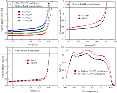 |
| | Fig. 4 (a) Current–voltage curves of FAPbI3 based devices. (b) Forward bias to short circuit (FB–SC) and short circuit to forward bias (SC–FB) current–voltage curves of FAPbI3 based devices without FAI/IPA modification. (c) Forward bias to short circuit (FB–SC) and short circuit to forward bias (SC–FB) current–voltage curves of FAPbI3 based devices with FAI/IPA modification. (d) The EQE spectra of the corresponding device A and B, respectively. | |
As we know, energy loss caused by charge recombination has an important influence on the device performance.34 Increased defects and trap density will increase the recombination centers of charge carriers, which will significantly decrease the value of JSC and FF.35 In order to investigate the charge recombination, steady state photoluminescence (PL) spectra were obtained for the same substrates. As shown in Fig. 5, the PL intensity of FAPbI3 film with FAI/IPA modification is higher than that without FAI/IPA modification. The results show that the non-radiative decay in FAPbI3 film is suppressed through FAI/IPA modification. As can be seen in Fig. 1, the PbI2 peak is eliminated and a much more pure FAPbI3 film formed with FAI/IPA modification. Herein, the decreased charge recombination rate indicates that the defects and trap density can be reduced in the improved FAPbI3 films, which leads to the increase of JSC and FF.
 |
| | Fig. 5 Steady-state PL intensity of FAPbI3 thin films on ITO/PEDOT:PSS surface (excitation wavelength: 680 nm). | |
Furthermore, the statistics of the PCE distribution from 40 devices are shown in Fig. 6. The Gaussian fit of the distribution is plotted for the histogram. As can be seen in Fig. 6a, the reproducibility of the device without surface modification is poor. The average PCE is only 8.53%, with about 65% of the devices having a PCE lower than 9%. The histograms (Fig. 6b) demonstrate that enhanced reliability and repeatability of the devices is achieved via FAI/IPA modification, and a PCE of over 12% is achieved for more than 60% of the devices. As far as commercialization is concerned, the stability of PSCs with FAI/IPA surface modification was investigated. The unencapsulated device was tested periodically in a glovebox, as shown in Fig. 7. The VOC and FF almost stay constant while the PCE retained 79.3% of its initial value even after being stored in a glovebox for 5 months. It can be seen that the degradation of PCE is mainly ascribed to the decreased JSC. One possible reason for such degradation could be interfacial degradation, i.e., PEDOT:PSS could etch ITO due to its acidic nature, which could cause degradation in long-term stability. The improved device stability is mainly ascribed to the improvement of the photoactive layer with surface modification. For further improvement of the stability, PSCs without the use of strongly acidic PEDOT:PSS are under way.
 |
| | Fig. 6 Statistics of the PCE for devices with and without FAI/IPA modification. Red and blue solid lines represent the Gaussian distribution fitting for the statistics of PCE. | |
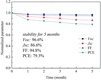 |
| | Fig. 7 Stability investigation of the unencapsulated perovskite solar cell stored in a glovebox. Normalized PCE, FF, VOC, and JSC versus time. | |
4. Conclusions
In this paper, we have demonstrated an inverted planar FAPbI3 based solar cell in which all layers were solution-processed without high temperature processes. By investigating the effect of FAI/IPA modification on FAPbI3 film and device performance, we found that smaller secondary grains grow on the surface of the film, that fill up the pinholes and cracks between grain boundaries, resulting in an improved coverage and thickness of the perovskite film. Besides, XRD patterns exhibit a purer crystalline phase, and non-radiative decay in the FAPbI3 film is significantly suppressed through FAI/IPA modification, all together leading to better light absorption, and therefore a higher current density as well as a better photovoltaic performance. Finally, the device with a PCE of up to 14.00% was obtained, and the devices exhibit good repeatability and long-term stability. These results show that simple FAI/IPA modification of the photoactive layer can greatly improve device performance for practical applications.
Acknowledgements
This work was supported by the National Natural Science Foundation of China (51573205, and 21274134), and Key Laboratory of Infrared Imaging Materials and Detectors, Shanghai Institute of Technical Physics, Chinese Academy of Sciences (IIMDKFJJ-14-08). X. Bao thanks the Youth Innovation Promotion Association CAS for financial support (2016194).
Notes and references
- A. Kojima, K. Teshima, Y. Shirai and T. Miyasaka, J. Am. Chem. Soc., 2009, 131, 6050–6051 CrossRef CAS PubMed
 .
. - H. Kim, C. Lee, J. Im, K. Lee, T. Moehl, A. Marchioro, S. Moon, R. Baker, J. Yum, J. Moser, M. Grätzel and N. Park, Sci. Rep., 2012, 2, 591 Search PubMed .
- W. Chen, X. Bao, Q. Zhu, D. Zhu, M. Qiu, M. Sun and R. Yang, J. Mater. Chem. C, 2015, 3, 10070–10073 RSC .
- S. Shi, Y. Li, X. Li and H. Wang, Mater. Horiz., 2015, 2, 378–405 RSC .
- M. Lee, J. Teuscher, T. Miyasaka, T. Murakami and H. Snaith, Science, 2012, 338, 643–647 CrossRef CAS PubMed .
- M. Liu, M. B. Johnston and H. Snaith, Nature, 2013, 501, 395–398 CrossRef CAS PubMed .
- O. Malinkiewicz, A. Yella, Y. Lee, G. Espallargas, M. Graetzel, M. Nazeeruddin and H. Bolink, Nat. Photonics, 2014, 8, 128–132 CrossRef CAS .
- J. Burschka, N. Pellet, S. Moon, R. Baker, P. Gao, M. Nazeeruddin and M. Grätzel, Nature, 2013, 499, 316–319 CrossRef CAS PubMed .
- N. Jeon, J. Noh, Y. Kim, W. Yang, S. Ryu and S. Seok, Nat. Mater., 2014, 13, 897–903 CrossRef CAS PubMed .
- J. Im, I. Jang, N. Pellet, M. Grätzel and N. Park, Nat. Nanotechnol., 2014, 9, 927–932 CrossRef CAS PubMed .
- M. Xiao, F. Huang, W. Huang, Y. Dkhissi, Y. Zhu, J. Etheridge, A. Gray Weale, U. Bach, Y. B. Cheng and L. Spiccia, Angew. Chem., Int. Ed., 2014, 126, 10056–10061 CrossRef .
- Q. Chen, H. Zhou, Z. Hong, S. Luo, H. Duan, H. Wang, Y. Liu, G. Li and Y. Yang, J. Am. Chem. Soc., 2013, 136, 622–625 CrossRef PubMed .
- P. W. Liang, C. Y. Liao, C. Chueh, F. Zuo, S. Williams, X. Xin, J. Lin and A. Jen, Adv. Mater., 2014, 26, 3748–3754 CrossRef CAS PubMed .
- W. Yang, J. Noh, N. Jeon, Y. Kim, S. Ryu, J. Seo and S. Seok, Science, 2015, 348, 1234–1237 CrossRef CAS PubMed .
- D. Bi, W. Tress, M. Dar, P. Gao, J. Luo, C. Renevier, K. Schenk, A. Abate, F. Giordano and J. Baena, Sci. Adv., 2016, 2, e1501170 Search PubMed .
- M. Saliba, T. Matsui, J. Seo, K. Domanski, J. Correa-Baena, M. Nazeeruddin, S. Zakeeruddin, W. Tress, A. Abate and A. Hagfeldt, Energy Environ. Sci., 2016, 9, 1989–1997 CAS .
- S. Pang, H. Hu, J. Zhang, S. Lv, Y. Yu, F. Wei, T. Qin, H. Xu, Z. Liu and G. Cui, Chem. Mater., 2014, 26, 1485–1491 CrossRef CAS .
- T. Koh, K. Fu, Y. Fang, S. Chen, T. Sum, N. Mathews, S. Mhaisalkar, P. Boix and T. Baikie, J. Phys. Chem. C, 2013, 118, 16458–16462 Search PubMed .
- N. Pellet, P. Gao, G. Gregori, T. Yang, M. K. Nazeeruddin, J. Maier and M. Grätzel, Angew. Chem., Int. Ed., 2014, 53, 3151–3157 CrossRef CAS PubMed .
- J. Lee, D. Seol, A. Cho and N. Park, Adv. Mater., 2014, 26, 4991–4998 CrossRef CAS PubMed .
- J. Wang, M. Qin, H. Tao, W. Ke, Z. Chen, J. Wan, P. Qin, L. Xiong, H. Lei and H. Yu, Appl. Phys. Lett., 2015, 106, 121104 CrossRef .
- J. M. Ball, M. M. Lee, A. Hey and H. Snaith, Energy Environ. Sci., 2013, 6, 1739–1743 CAS .
- F. Di Giacomo, S. Razza, F. Matteocci, A. D’Epifanio, S. Licoccia, T. Brown and A. Carlo, J. Power Sources, 2014, 251, 152–156 CrossRef CAS .
- Y. Zhang, W. Liu, F. Tan and Y. Gu, J. Power Sources, 2015, 274, 1224–1230 CrossRef CAS .
- N. Jeon, H. Lee, Y. Kim, J. Seo, J. Noh, J. Lee and S. Seok, J. Am. Chem. Soc., 2014, 136, 7837–7840 CrossRef CAS PubMed .
- W. Ke, G. Fang, J. Wang, P. Qin, H. Tao, H. Lei, Q. Liu, X. Dai and X. Zhao, ACS Appl. Mater. Interfaces, 2014, 6, 15959–15965 CAS .
- J. Heo, H. Han, D. Kim, T. Ahn and S. Im, Energy Environ. Sci., 2015, 8, 1602–1608 CAS .
- D. Yuan, A. Gorka, M. Xu, Z. Wang and L. Liao, Phys. Chem. Chem. Phys., 2015, 17, 19745–19750 RSC .
- X. Bao, Q. Zhu, M. Qiu, A. Yang, Y. Wang, D. Zhu, J. Wang and R. Yang, J. Mater. Chem. A, 2015, 3, 19294–19298 CAS .
- M. Leyden, M. Lee, S. Raga and Y. Qi, J. Mater. Chem. A, 2015, 3, 16097–16103 CAS .
- G. Eperon, S. Stranks, C. Menelaou, M. Johnston, L. Herz and H. Snaith, Energy Environ. Sci., 2014, 7, 982–988 CAS .
- G. Eperon, D. Bryant, J. Troughton, S. Stranks, M. Johnston, T. Watson, D. Worsley and H. Snaith, J. Phys. Chem. Lett., 2014, 6, 129–138 CrossRef PubMed .
- X. Bao, Y. Wang, Q. Zhu, N. Wang, D. Zhu, J. Wang, A. Yang and R. Yang, J. Power Sources, 2015, 297, 53–58 CrossRef CAS .
- J. Krüger, R. Plass, C. Le, M. Piccirelli, M. Grätzel and U. Bach, Appl. Phys. Lett., 2001, 79, 2085–2087 CrossRef .
- R. Street, Adv. Mater., 2016, 28, 3814–3830 CrossRef CAS PubMed .
|
| This journal is © The Royal Society of Chemistry 2016 |
Click here to see how this site uses Cookies. View our privacy policy here. 


