DOI:
10.1039/C6RA15005E
(Paper)
RSC Adv., 2016,
6, 72634-72642
Electronic properties of a pristine and NH3/NO2 adsorbed buckled arsenene monolayer
Received
9th June 2016
, Accepted 15th July 2016
First published on 15th July 2016
Abstract
Analogous to exfoliated 2D sheets of black phosphorene, arsenene is an atomically thin layer of the arsenic crystal. In this paper, we investigate the sensitivity of a pristine arsenene sheet for NH3 and NO2 molecules in terms of binding energy, nature of bonding, density of states and current–voltage characteristics. The calculated results based on density functional theory find that both NH3 and NO2 molecules show a significant affinity for arsenene leading to strong physisorption with significant electronic charge transfer. The calculated I–V characteristics reveal that physisorption of NH3 and NO2 induces modifications in the conductivity of pristine arsenene. Incorporation of Ge in arsenene leads to enhanced binding of NH3 and NO2 via chemisorption on arsenene.
1 Introduction
In the last few years great attention has been paid to atomically thin layers of group V elements. In this quest, researchers have studied phosphorene (obtained from phosphorus) more extensively.1–3 Recently, the experimental existence of black phosphorene and theoretical prediction of blue phosphorene have been confirmed. Subsequently this single layered novel nanostructure further fascinated researchers to look for other possible quasi 2D-nanosheets of group V-elements. In this race, analogous to exfoliated 2D nanosheets of silicene, germenene, phosphorene, arsenene, antimonene and stanane are proposed. Although graphene is not found to be an effective adsorbent for small organic molecules like ammonia, acetone, acetonitrile, benzene, methane, methanol, ethanol, and toluene. Comparatively these rippled surfaces of silicene and germenene are good adsorbent.4,5 Silicene and germenene is zero band semiconductor and adsorption of such organic molecule generally introduced opening of band gap. Several works suggest that these quasi 2D materials show quantum spin Hall effect (QSH) transistor behaviour on functionalization, followed by straining.6–8 Such QSH two dimensional topology play important role in spintronic devices. The structural and electronic properties of arsenene and antimonene (from antimony) have been characterized9–11 using first principles methods. Kamal et al.9 claimed for the arsenene in puckered phase as stable configuration compare to buckle one. Their phonon calculations for buckled arsenene resulted imaginary frequency near Γ point for transverse acoustic mode, and anticipated it as reason of some computational disparity. Contrary to this Zhang et al.10 have reported a stable buckled phase with no imaginary frequency found in phonon calculation. These research efforts although addresses well the structural and electronic characterization but didn't discuss its any applications. On other hand in the last few years, efforts have been made to look at the better 1D or 2D nanomaterial for sensing the toxic gases/chemicals in its surroundings. Hence, we thought it is pertinent to explore the possibility of arsenene as relatively better sensing material than existing carbon allotropes for molecules of ammonia (NH3), and nitrogen dioxide (NO2). It is well established fact that NH3 and NO2 are products of various chemical and biological processes and are considered to be hazardous. For example, NH3 is generally found in common industrial environment and NO2 is primarily emitted by motor vehicles. NO2 is also precursor for a number of harmful secondary air pollutants like nitric acid, aerosols and photo oxidants. Previously, sensing characteristics of the well-known 1D and 2D carbon allotropes, through adsorption analysis have been extensively reported by our group12–19 as well as by others.20–24 In present work we intentionally examine the buckled phase arsenene for NH3 and NO2 molecule. We also investigate the possibility of the arsenene-based devices for applications in sensing of toxic gases.
First ground state calculations under self-consistent field are performed to obtain minima at potential energy surface for pristine buckled arsenene sheet. Subsequently, analysis of structural parameter and electronic properties like phonon spectra, natural bond orbital (NBO),25 density of state (DOS), bandstructure, highest occupied molecular orbital (HOMO) and the lowest unoccupied molecular orbital (LUMO) are scrutinized. To check the convergence of employed theory for present work, structural and electronic characterization and its comparison with other findings9,10 have been reported at the initial stage of work. The sensitivity of arsenene towards NH3 and NO2 molecules has been analyzed in terms of binding energy, charge transfer, DOS, charge decomposition analysis (CDA) and current–voltage characteristic (I–V). We also consider the case of Ge-doped arsenene to determine the relationship between the affinity of molecules and dopant in the 2d lattice.
2 Computational method
Electronic calculations have been performed in the framework of density functional theory (DFT) using Gaussian09 (G09).26 Additionally, we employed the Atomistix-tool-kit Virtual nanolab (ATK-VNL) program package27 to investigate properties of arsenene-based device consisting of a quasi 2D-sheet. Fig. 1 display the optimized cluster and periodic buckled arsenene: a finite cluster model for G09 calculations and a periodic supercell model for ATK-VNL calculations are considered. The cluster model consists of 54 As-atoms with hydrogen passivation at edge atoms. In G09 calculations, the generalized exchange correlation in terms of Perdrew–Burke–Ernzherof (PBE)28 type parameterization along with the 6-31g(d) basis sets are used. Frequency calculations are performed to ascertain the ground state configuration of the system. DOS and CDA calculations have been performed using G09 output within AOMix29–35 software package. For ATK calculations, the PBE-DFT approximation along with the double-ζ-polarized (DZP) basis set and Troullier–Martins36 pseudo-potentials are considered. Split-valence double-ζ-polarized basis set are sufficient for computational convergence. The norm-conserving Troullier–Martins pseudo-potential describes the interaction between ionic cores and localized pseudo-atomic orbitals. A (14.4 Å × 14.4 Å × 15 Å) supercell having 32 As atoms is chosen. The distances between periodic images of arsenene are kept at 15 Å to avoid interlayer interaction. The sampling of reciprocal space with (8 × 8 × 1) k-points is made using Monkhorst–Pack scheme37 for geometry optimization, while k-point sampling are set at 16 × 16 × 1 for calculations of electronic properties. For odd electronic configuration of NO2-arsenene sheet, spin-polarized calculations have been performed. The combination of DFT and Non-Equilibrium Green's Function (NEGF) method38 in ATK-VNL is made to derive electron transport calculations. This calculation is important for finding transmission spectra at different bias windows its derivative current–voltage (I–V) characteristics.
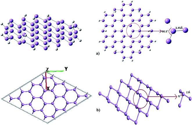 |
| | Fig. 1 (a) Finite cluster and (b) periodic supercell representing single layer arsenene sheet. | |
3 Results and discussion
3.1 Pristine arsenene
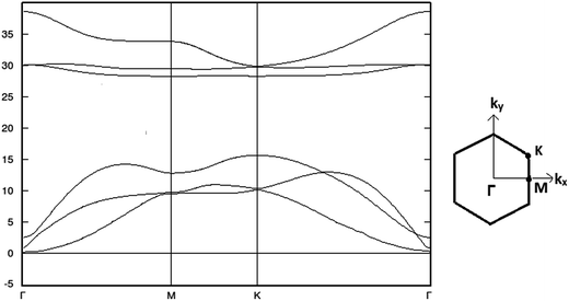
The stability of buckled arsenene has been confirmed through phonon calculations and thus validates the employed theoretical approach for further investigations. No imaginary frequencies were found. Likewise, Fig. 2 shows no soft modes confirming the stability of arsenene. Additionally, the convergence of geometrical parameters for arsenene from the cluster (G09) and the periodic supercell (ATK) approaches signify the appropriateness of these approaches in our work. For example, the calculated As–As bond length is 2.45 Å from G09 and is 2.5 Å from ATK. The calculated bond angle between adjacent atoms (<As–As–As) are 90.5° and 91° obtained from G09 and ATK, respectively. Table 1 lists the measured bond-length and bond-angles of arsenene along with the calculated values from previous reports. The calculated band structure, shown in Fig. 3, exhibits an indirect band gap of 1.83 eV which lies in-between the calculated values of 1.635 eV (ref. 9) and 2.28 eV.10 From the device point of view to exploit the buckled arsenene as conducting channels, it must have high electron mobility which is inversely proportional to its effective mass.39 The effective mass of electron (me) is calculated to be 0.18m0 and 0.52m0 for Γ–K and Γ–M directions, respectively, assuring high mobility of electrons along these particular directions.
 |
| | Fig. 2 Calculated phonon dispersion curves along high symmetry direction in the periodic supercell model. | |
Table 1 Geometrical parameters of optimized arsenene through G09 and ATK package along with earlier reports
| Geometrical parameters |
G09 |
ATK |
Earlier findings |
| Bond-length (As–As) |
2.45 Å |
2.5 Å |
2.50 Å (ref. 4), 2.45 Å (ref. 5) |
| Bond angle (<As–As–As) |
90.5° |
91° |
92.2° (ref. 4), 92.5° (ref. 5) |
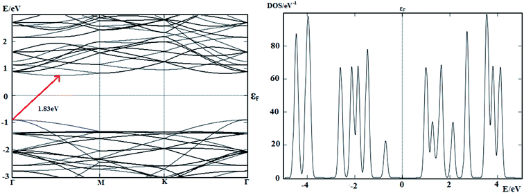 |
| | Fig. 3 Calculated band structure and DOS of arsenene in the periodic supercell model. | |
Similar to blue phosphorene, atoms in arsenene have sp3 character at lattice point. The NBO analysis reveals that the lone pair electrons are mainly localized on 4s-subshell and the 4p electrons are engaged in the σ-bonding formation. The inter-frontier orbital analysis confirms that HOMO is delocalized with contributions from σ- and lone pair electronic density (Fig. 4a). On the other hand, localized LUMO is primarily σ* in nature (Fig. 4b) for arsenene. From molecular orbital diagram it is clear that electronic charge is mainly localized on atomic center which make arsenene different from graphene. In graphene C-atoms are present at vertex of two dimensional honey comb lattice structure, this planarity enhance conjugation in between adjacent bond and results in delocalization of electronic density. Contrary, in the arsenene lattice As atoms are in two different planes (up and own), in each ring which inhibit such conjugation effects.
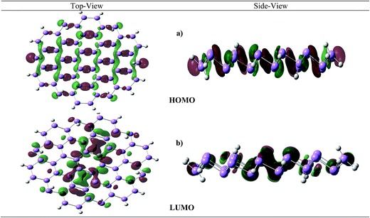 |
| | Fig. 4 Electronic charge density associated with the inter-frontier orbitals of arsenene. | |
3.2 NH3 and NO2 adsorbed arsenene
To investigate the NH3 and NO2 adsorption on arsenene, several possible adsorption sites including top of the each atoms, centre of As–As bond and centre of the hexagonal ring have been considered. Fig. 5(i), depict different orientation of NH3/NO2 considered over arsenene sheet before optimization at reasonable distance. For present context, NH3 and NO2 affinity towards arsenene surface is analysed in terms of adsorbate (NH3/NO2) and adsorbent interaction i.e., adsorption. The phenomenon of adsorption plays an important role in understanding sensitivity of surface towards exotic molecules. If adsorption is strong i.e. by means of charge transfer interaction this may be label as chemisorption. Comparatively physisorption has nothing to do with charge transfer mechanism and interaction between adsorbate and adsorbent is via van der Waals forces. Typically interaction energy in this case lies in-between 0.01 eV to 0.1 eV.40 For NH3, the ground state calculation reveals N pointing to arsenene surface with hydrogen atoms on next end as preferred orientation of the molecule. Likewise, N at the centre of symmetrical O–N–O bond actively participates with arsenene. The preferred site for NH3 was found to be centre of ring as shown in Fig. 5 with the adsorption energy of 0.87 eV. Here, N atom was symmetrically away from upper layer arsenene atom with the bond distance of 3.01 Å. In contrary, Wang et al.4 reported NH3 is comparatively less bonded with germenene having binding energy of −0.459 eV with N pointing towards one of Ge atom. Both NBO analysis and molecular orbital density contour plots suggested noticeable interaction between NH3 and arsenene. The lone pair orbital at N of NH3, donates a partial charge of about 0.11e to arsenene, thus NH3 brings changes in electronic density of the inter-frontier orbitals associated to arsenene sheet. The HOMO–LUMO gap is now reduced to 2.4 eV for the arsenene sheet. NO2 adsorbed configuration of arsenene exhibits lowering of inter-frontier orbital to 2.23 eV for spin-up states and 0.79 eV for spin-down states. This change in orbital energy levels can be seen as intimacy of arsenene towards NO2. The contour plots at 0.04e per Å3 shown in Fig. 5 depict overlapping of the empty valence p-orbital of N from NO2 with non-bonding lone pair orbitals of arsenene. This overlapping is missing for NH3 molecules in present contour context. The reason could be inter-electronic repulsion between NH3 and arsenene lone pair electronic cloud. The calculated PDOS (Fig. 6) verify these contour plots in concern of N-valence p orbital from NH3, NO2 and geometrically closed As from arsenene. The active participation of these fragments at inter-frontier orbital sites could be observed.
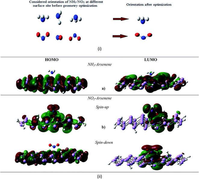 |
| | Fig. 5 (i) Different NH3/NO2 orientation considered towards arsenene sheet and (ii) electronic charge density associated with the inter-frontier orbitals of (a) NH3-arsenene and (b) NO2-arsenene. | |
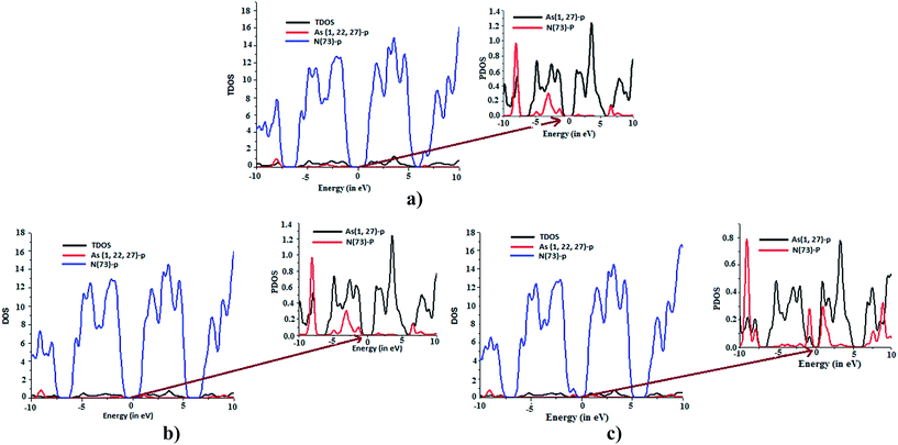 |
| | Fig. 6 Calculated DOS for adsorbate and adsorbent (a)NH3-arsenene, (b) and (c) for up and down spin states for polarized NO2-arsenene calculations, respectively. | |
The ATK calculated electronic properties also show resemblance to the G09 calculated electronic properties suggesting a convergence of finite cluster and periodic supercell approach for present arsenene model. Note that both finite cluster and periodic supercell approaches find a feeble affinity of NH3 and NO2 towards arsenene.
3.3 Charge decomposition analysis
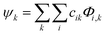
To get a detailed insight into bonding characteristics of the adsorbed arsenene system, we now perform charge decomposition analysis of the system. The fragmentation of adsorbate (second fragment orbital (2nd FO)) and adsorbent (first fragment orbital (1st FO)) of adsorbate + adsorbent (whole) and further derivation of wave functions for the whole from 1st and 2nd FO as their linear combination35 calculated in CDA analysis.41,42 kth molecular orbital Ψk of whole system represented as,| |
 | (1) |
Φi,k is ith fragment orbital of kth fragments with k = 1, 2 and cik is fragment orbital coefficients. For the NH3 adsorbed arsenene, the CDA analysis suggests the presence of a charge interaction which is mainly governed by mixing of occupied molecular orbital of one fragment with unoccupied of other. This computes the mode of interaction is via strong physisorption, where small self-polarizations of fragments in presence of each other have insignificant contribution. Similarly, a close inspection by performing CDA on NO2 adsorbed arsenene finds spin-up states with 0.06e charge transfer from NO2 to arsenene. This is not the case with spin-down states where NO2 gains 0.16e from arsenene, resulting in total charge transfer of 0.95e between sheet and NO2. Since self polarization for spin-up states are more prominent compare to spin-down states, the mode of adsorption appears to be a strong physisorption or quasi chemisorption of gas molecules on arsenene.
3.4 Arsenene-based device: current–voltage characteristics
The above discussion is mainly focused on electronic analysis for NH3 and NO2 affinity for arsenene surface. These adsorption induced charge transformation should lead to the conductivity variation of the adsorbent. To investigate such variation in conductivity, the NEGF method has been employed to compute the transmission spectra at different bias voltage across the arsenene in two probe device models. Subsequently, the current–voltage characteristics are drawn from the calculated transmission coefficients.
The transmission function of a system is sum of transmission probabilities of all channels that particularly being results due to external bias (V), represented as
| | |
T(E, V) = Tr[ΓL(E, V)GR(E, V)ΓR(E, V)GA(E, V)]
| (2) |
GR/A is retarded and advanced Green's functions and coupling functions ΓL/R represent imaginary part of left and right self energies, respectively. This expression is further introduced to Landuer–Bittier Formula43 to evaluate the current as integration of the transmission function over the bias window near the Fermi level:
| |
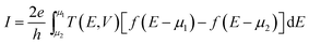 | (3) |
f(
E −
μ1/2) is Fermi distributions functions of electrons in left or right electrodes and
μ1/2 are chemical potentials of left and tight electrodes.
Although the model arsenene possess structural anisotropy, in our analysis we have considered orthogonal in plane direction to armchair one, i.e. edged As-atoms on arsenene sheet have zig–zag arrangement along the length of model device. Two-probe models were used with semi-infinite left and right electrode regions in contact with the central region shown in Fig. 7. The length of each electrode and the central scattering region is ≈14 A along z-axis. Application of the external field to electrodes results in shifting of Fermi level. Matching of the valance band maxima of left electrode with the conduction band minima of right electrode generally leads to flow of current in the device.
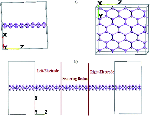 |
| | Fig. 7 Schematic of two probe device model for arsenene. (a) Electrode and (b) device consisting of electrodes and scattering regions. | |
Fig. 8 and 9 show the transmission spectra of pristine arsenene derived current at different bias voltage up to 8 V, respectively. There is a negative differential resistance (NDR) region found for all three cases suggesting this as signature of the pristine arsenene. To cross check any numerical convergence artefact that might consequence to NDR, negative biases were also applied across the electrode in the pristine arsenene device model, which completely rule out our perception. For the pristine arsenene, the I–V curve (Fig. 9) suggests that there is no current till 4.8 V. This threshold value of the applied bias is larger than the calculated bandgap of 1.73 V and can be seen for elucidation of high localized electronic charge in the 2d lattice. After the bias of 4.8 V, a significant current flows through the device rising upto 12.3 nA at 6 V. However beyond this bias voltage, the negative resistance behaviour of arsenene device model is exhibited till 6.7 V. Further rise in applied bias yields into a nonlinear behaviour of the current–voltage characteristics. The presence of NH3 molecule results in increased resistivity of arsenene sheet by inhibiting conduction channel across the Fermi level as is evident from Fig. 8b. At applied voltage of about 7.2 V, significant current begin to observe and afterwards the current voltage relation follow Ohmic behaviour in NH3 sense arsenene model. Compare to NH3, NO2 presence on arsenene relatively increased conductivity but for the same transmission spectra plotted as Fig. 8c doesn't convey any information. It is expected that withdrawing nature of NO2 change the arsenene surface to p-type semiconductor resulting in the enhanced conductivity.44
 |
| | Fig. 8 Transmission spectra at different applied bias voltage for (a) arsenene, (b) NH3-arsenene and (c) NO2-arsenene. | |
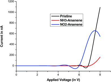 |
| | Fig. 9 I–V relationship for pristine and NH3/NO2 exposed arsenene sheet. | |
3.5 Ge-doped arsenene
The electronic properties of arsenene are found to be sensitive to adsorption of NH3 or NO2 molecules. In order to increase the sensitivity, we have investigated effect of doping Ge to arsenene surface. The choice of Ge as dopant relies on its electron deficient nature compare to As atoms and can make the doping sites chemically active. The following brief descriptions address Ge doping effect on NH3/NO2.
Fig. 10 shows the equilibrium configurations of NH3 and NO2 adsorbed on Ge-doped arsenene. The NBO analysis suggests NH3 get intact to arsenene with a charge transfer of 0.22e in terms of natural atomic charges calculated in NBO analysis with a binding energy of −1.13 eV. As evident from Fig. 10a DOS analysis shows lone pair electrons localized at 2pz orbital get depopulated by electronic charge transfer to 4pz of Ge at HOMO of spin-up state. However for spin-down state calculations, the hybridization between these mentioned orbital fragments take place at LUMO (Fig. 10b). The binding energy for NO2 is found to be −2.9 eV, with one of O atom gets bonded to Ge with bond length 1.98 Å. The strong binding between Ge and O can be attributed from the Ge–O bond length, which has electronic population of 1.96e and is consequence of strong electron dispersion on Ge from NO2 also evident from Fig. 10c in terms of orbital hybridization.
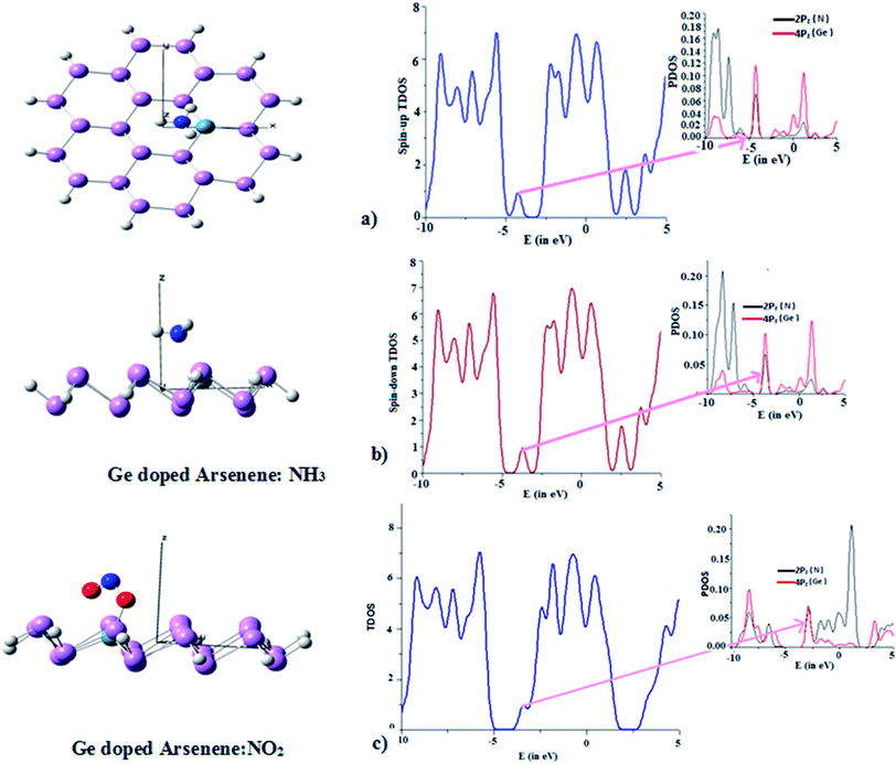 |
| | Fig. 10 Optimized configuration and DOS of (a) NH3 and (b) NO2 adsorbed Ge doped arsenene. | |
4 Conclusions
In this work we performed theoretical analysis of newly proposed 2D monolayer of arsenene using DFT approach. Analysis suggests that proposed quasi 2D-sheet is stable and showing semiconducting behaviour. Where, NH3 and NO2 adsorbed at arsenene surface with significant binding energy of 0.87 eV and 0.81 eV, respectively, computed through G09 which very close to with ATK-VNL calculations. Mulliken and NBO charges suggest significant amount of electronic charge transfer in between gas molecules and arsenene. CDA, PDOS and molecular orbital diagram provide considerable evidence for binding of NH3 and NO2 at the quasi 2D-surface. The sensitivity of arsenene surface for NH3 and NO2 further have been analyzed in terms of I–V characteristic using NEGF method. The obtained result exhibits lowering of conductivity across the nanosheet surface on sensing NH3. Contrary, NO2 sensing made the sheet slightly more conductive in nature and is effect of electron withdrawing nature of NO2. Ge substituted on arsenene indicate strong adsorption of NH3 and NO2 molecule.
Acknowledgements
Authors are thankful to ABV-IIITM, Gwalior for providing the computational resources to perform the simulation work. One of us Md. Shahzad Khan is thankful to DST, Nano Mission for providing the Research Associateship.
References
- L. Li, Y. Yu, G. J. Ye, Q. Ge, X. Ou, H. Wu, D. Feng, X. H. Chen and Y. Zhang, Nat. Nanotechnol., 2014, 9, 372–377 CrossRef CAS PubMed.
- H. Liu, A. Neal, Z. Zhu, Z. Luo, X. Xu, D. Tomanek and P. D. Ye, ACS Nano, 2014, 8, 4033–4041 CrossRef CAS PubMed.
- L. Kou, C. Chen and S. C. Smith, J. Phys. Chem., 2015, 6, 2794–2805 CAS.
- Y. P. Wang, W. X. Ji, C. Zhang, S. Li, F. Li, P. Li, M. J. Ren, X. L Chen, M. Yuan and P. Wang, Mater. Chem. Phys., 2016, 173, 379–384 CrossRef CAS.
- W. Hu, N. Xia, X. Wu, Z. Li and J. Yang, Phys. Chem. Chem. Phys., 2014, 16, 6957–6962 RSC.
- Y. P. Wang, C. W. Zhang, W. X Ji, R. W Zhang, P. Li, P. Wang, M. Ren, X. L. Chen and M. Yuan, J. Phys. D: Appl. Phys., 2016, 49, 055305 CrossRef.
- Y. P. Wang, W. X. Ji, C. W. Zhang, P. Li, F. Li, M. Ren, X. Li Chen, M. Yuan and P. Wang, Sci. Rep., 2016, 6, 20342 CrossRef CAS PubMed.
- Y. P. Wang, W. X. Ji, C. W. Zhang, P. Li, F. Li, P. J. Wang, S. S. Li and S. S Yan, Appl. Phys. Lett., 2016, 108, 073104 CrossRef.
- C. Kamal and M. Ezawa, Phys. Rev. B: Condens. Matter Mater. Phys., 2015, 91, 085423 CrossRef.
- S. Zhang, Z. Yan, Y. Li, Z. Chen and H. Zeng, Angew. Chem., 2015, 10, 3112–3115 CrossRef PubMed.
- Z. Zhang, J. Xie, D. Yang, Y. Wang, M. Si and D. Xue, Appl. Phys. Express, 2015, 8, 055201 CrossRef.
- A. Tyagi, V. Sharma and A. Srivastava, Adv. Sci. Lett., 2014, 20, 1570–1573 CrossRef.
- A. Srivastava, C. Bhat, S. K. Jain, P. K. Mishra and R. Brajpuriya, J. Mol. Model., 2015, 21, 1–8 CrossRef PubMed.
- A. Srivastava, V. Sharma, K. Kaur, M. S. Khan, R. Ahuja and V. K. Rao, J. Mol. Model., 2015, 21, 1–7 CrossRef PubMed.
- M. S. Khan, A. Srivastava, R. Chauraiya, M. S. Khan and P. Dua, Chem. Phys. Lett., 2015, 636, 103–109 CrossRef CAS.
- A. Srivastava, M. S. Khan, S. K. Gupta and R. Pandey, Appl. Surf. Sci., 2015, 356, 881–887 CrossRef CAS.
- R. Chandiramouli, A. Srivastava and V. Nagarajan, Appl. Surf. Sci., 2015, 351, 662–672 CrossRef CAS.
- S. K. Jain and A. Srivastava, Adv. Sci. Lett., 2014, 20, 1624–1630 CrossRef.
- B. Anand, M. Karakaya, G. Prakash, S. S. S. Sai, R. Philip, P. Ayala, A. K. Sood, A. Srivastava, A. Rao and R. Podila, RSC Adv., 2015, 5, 59556–59563 RSC.
- G. Ko, H.-Y. Kim, J. Ahn, Y.-M. Park, K.-Y. Lee and J. Kim, Curr. Appl. Phys., 2010, 10, 1002–1004 CrossRef.
- H. J. Yoon, D. H. Jun, J. H. Yang, Z. Zhou, S. S. Yang and M. M. Cheng, Sens. Actuators, B, 2011, 157, 310–313 CrossRef CAS.
- M. Kharatha, A. Vaez, A. Seyed and H. Rozatian, Mol. Phys., 2013, 111, 3726–3732 CrossRef CAS.
- Y.-H. Zhang, Ya-B. Chen, K.-G. Zhou, C.-H. Liu, J. Zeng, H.-L. Zhang and Y. Peng, Nanotechnology., 2009, 18, 185504 CrossRef PubMed.
- A. E. Reed, L. A. Curtiss and F. Weinhold, Chem. Rev., 1988, 88, 899–926 CrossRef CAS.
- M. J. Frisch, et al., Gaussian09, Revision A.02, Gaussian, Inc., Wallingford CT, 2009 Search PubMed.
- http://www.quantumwise.com.
- J. P. Perdrew, K. Burke and M. Ernzerhof, Phys. Rev. Lett., 1997, 78, 1396 CrossRef.
- S. I. Gorelsky, AOMix: Program for Molecular Orbital Analysis, York University, Toronto, 1997 Search PubMed.
- S. I. Gorelsky and A. B. P. Lever, Organomet. Chem., 2001, 635, 187–196 CrossRef CAS.
- E. I. Solomon, S. I. Gorelsky and A. Dey, J. Comput. Chem., 2006, 27, 1415–1428 CrossRef CAS PubMed.
- W. Macyk, K. Szacilowski, G. Stochel, M. Buchalska, J. Kuncewicz and P. Labuz, Coord. Chem. Rev., 2010, 254, 2687–2701 CrossRef CAS.
- A. Srivastava, Md. S. Khan, S. K. Gupta and R. Pandey, Appl. Surf. Sci., 2015, 356, 881–887 CrossRef CAS.
- M. S. Khan and M. S. Khan, Int. Nano Lett., 2012, 2, 1–7 CrossRef.
- M. S. Khan and M. S. Khan, Phys. E, 2012, 44, 1857–1861 CrossRef CAS.
- N. Troullier and J. L. Martins, Phys. Rev. B: Condens. Matter Mater. Phys., 1991, 43, 1993 CrossRef CAS.
- M. Brandbyge, J. L. Mozos, P. Ordejon, J. Taylor and K. Stokbro, Density functional method for nonequilibrium electron transport, Phys. Rev. B: Condens. Matter Mater. Phys., 2002, 65, 165401 CrossRef.
- S. Datta, Quantum Transport: Atom to Transistor, Cambridge University, Press, Cambridge, UK, 2005 Search PubMed.
- M. G. Silveirinha and N. Engheta, Phys. Rev. B: Condens. Matter Mater. Phys., 2012, 86, 161104 CrossRef.
- H. Luth, et al., Surfaces and interfaces of solids, Springer-Verlag, 1993, ISBN 978-3-540-56840-7 Search PubMed.
- S. I. Gorelsky and E. I. Solomon, Theor. Chem. Acc., 2008, 129, 57–65 CrossRef.
- S. Dapprich and S. G. J. Frenking, J. Phys. Chem., 1995, 99, 9352–9362 CrossRef CAS.
- G. Frenking and N. Frohlich, Chem. Rev., 2000, 100, 717–774 CrossRef CAS PubMed.
- H. D. Cornean, A. Jensen and V. Moldoveanu, J. Math. Phys., 2005, 46, 042106 CrossRef.
- H. Bai and G. Shi, Sensor, 2007, 7, 267–307 CrossRef CAS.
|
| This journal is © The Royal Society of Chemistry 2016 |
Click here to see how this site uses Cookies. View our privacy policy here. 


