DOI:
10.1039/C6RA14836K
(Paper)
RSC Adv., 2016,
6, 73790-73796
Controlled electrochemical and electroless deposition of noble metal nanoparticles on graphene†
Received
7th June 2016
, Accepted 25th July 2016
First published on 25th July 2016
Abstract
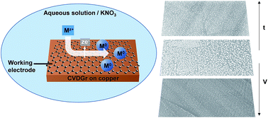
Electrodeposition of nanoparticles on graphene is described, providing a convenient approach for making graphene–nanoparticle composites as well as insight into the electrochemical activity of graphene. To avoid complications due to surface contamination, chemical vapour deposition grown graphene was used directly on its copper growth substrate. We identify and isolate two nanoparticle growth processes for both silver and palladium deposition: electroless deposition that appears to occur preferentially at defects and edges next to the underlying copper, and conventional electrodeposition that occurs uniformly across the graphene surface. We show that control over electrodeposited nanoparticle size and number density can be achieved through varying electrodeposition conditions. The resultant nanoparticles are homogeneously dispersed across the graphene surface, suggesting that here both edge-plane and basal-plane graphene sites are electroactive. These results demonstrate that, as with other carbon nanostructures, electrodeposition is a powerful and flexible tool for forming functional composites with graphene.
Introduction
Metal nanoparticles (NPs) are of great interest because of their unique catalytic and sensing properties.1–3 However, the properties are tightly correlated with their size and morphology, and in addition, the dispersion of NPs onto appropriate substrates is a prerequisite for their implementation in practical devices.4 Electrodeposition is a particularly interesting route to forming NPs structures, since by careful choice of the substrates and electrochemical parameters (i.e. applied potential, electrodeposition time, analyte concentration), it is possible to control the size and morphology of the grown NPs.5–8
Carbon nanostructures such as carbon nanotubes (CNTs), high oriented pyrolytic graphite (HOPG) or graphene (Gr) have been widely explored as supports for the deposition and/or electrodeposition of NPs.5–16 These three allotropes each have conjugated sp2 carbon arranged in a hexagonal lattice, but each with a different geometry. Gr is a two dimensional material only a single layer thick, while HOPG is a 3D structure formed from regularly stacked Gr layers,17 and CNTs are a one dimensional material which result from rolling up Gr sheets into closed cylinders.18 The sp2 structure of these materials confers on them electronic properties which are appropriate for the development of nanoscopic electrodes. In fact, the use of HOPG as an electrode for the deposition of metal NPs has been known for a long time. Of particular interest is the work by Penner's group on the mechanism of electrodeposition of a variety of metal NPs onto HOPG electrodes.7–9,19 This work sets the scene for the utilization of other low dimensional carbon nanostructures (i.e. CNTs and Gr) as electrode materials for the electrodeposition of metal NPs. According to Penner et al. the growth of metal NPs onto HOPG is characterized by a rapid nucleation, followed by a progressive growth of NPs, which means that the growth is initially controlled by kinetics and then is diffusion limited. A similar trend has been observed by Macpherson's group when using CNTs as electrode material for the creation of metal nanowires.5,20–22 In fact, Macpherson was able to control size, particle distribution and particle density by varying deposition time and applied potential,5 similar to Penner's work on HOPG.9,19 To date, though, similar use of electrodeposition on Gr has been complicated by the several methodologies employed for its synthesis, which result in a variety of Gr with varying structural and chemical properties.23–25
Graphene can be obtained either following top-down (e.g. synthesis by reduction of graphene oxide)23,26–28 or bottom-up methodologies (e.g. chemical vapour deposition of Gr).24,29,30 The synthesis of Gr from the reduction of graphene oxide provides bulk quantities of a highly defective Gr material, usually referred to as reduced graphene oxide (rGO). Although electrodeposition has been employed to further modify rGO,31–33 its intrinsic defects complicate the study of the fundamentals of electrodeposition on graphene. Chemical vapour deposition (CVD), on the other hand, is a promising route to the formation of large area, high quality graphene. Gr is formed by CVD through the decomposition of a carbon feedstock over a metallic substrate, typically nickel or copper, at high temperature. The use of copper substrates, rather than nickel, has proven to be more effective in achieving monolayer Gr of large grain size. As a result, the properties of monolayer CVD-Gr on copper are comparable to those of mechanically exfoliated graphene.29 However, the use of CVD-Gr grown on copper for electrochemical investigations has been hampered by the reactivity of copper itself, and the need to transfer Gr to an insulating substrate as a step prior to any electrochemical process.34–42 The transferring process typically involves the use of polymer layers and metal etchants that lead to surface contaminants on the lattice of graphene.41,43 Those contaminants play a major role in the final electrochemical behaviour and thus,40,44–46 are undesirable for such studies. We have recently shown how electrochemical experiments can be directly made on CVD-Gr on copper, making quick cheap and reproducible graphene electrodes.47 In this paper we extend this approach and demonstrate for the first time how metal NPs can be grown directly on CVD-Gr under electrochemical control; we isolate electroless and electrodeposition processes and show that the electrodeposition proceeds with a similar mechanism to that previously observed on HOPG and CNT, opening the way to using established approaches for the controlled electrochemical modification of graphene.
Experimental methods
Low-pressure CVD of graphene on copper
Gr was grown on copper foil using a low-pressure CVD system as described previously.48 In brief, copper foil substrates (99.5% purity, 0.025 mm thick, Alfa Aesar product number 13382) were cleaned by electrochemical polishing and washing, following the procedure described by Miseikis et al.49 Using a 1 inch tube furnace pumped to low pressure by a turbomolecular pump, the foil was heated to 1000 °C and annealed for 20 minutes prior to growth. A hydrogen flow was maintained throughout the process, with methane introduced for the growth stage. The standard growth conditions used were 10 standard cubic centimetres (sccm) of hydrogen, with 2.5 sccm of methane and a growth time of 20 minutes. For partial coverage samples the growth time was reduced to 10 minutes. After cooling to room temperature, the Gr on copper samples were removed from the furnace and stored under ambient conditions before use.
Raman spectroscopy and scanning electron microscopy (SEM)
Raman spectra were recorded with a Renishaw InVia micro-Raman system using a 514 nm laser excitation, with a laser power of ca. 5 mW. A confocal microscope with 50× lens was used to record spectra at a spatial resolution of ∼2 μm. SEM characterization was performed on a ZEISS Supra 55-VP field emission SEM, operated at 10 kV, using the inLens secondary electron detector. Raman and SEM analysis were performed on the Gr on copper foils as grown. ImageJ50 was used to analyse the SEM images (Fig. SI2†) and quantify the coverage of the samples and the size of the grown nanoparticles (see Fig. SI3†).
Electrochemical processes
BST8-stat instrument from MTI KJ group was used to record cyclic voltammograms (CVs). A three-electrode configuration was used, where CVD-Gr on copper was the working electrode. To achieve a constant surface area for the electrode, each sample was masked with a piece of 3M Model 470 Electroplater tape with a pre-cut 0.05 cm2 hole. A GAMRY electrochemical cell (model PTC1 paint test cell) was clamped to the working electrode (see ESI1†). As reference electrode and counter electrode a GAMRY Ag/AgCl (in saturated KCl) and a Pt wire were used, respectively. For the electrodeposition process the system was set up in time base mode. In a typical electrodeposition experiment the potential was fixed at −0.4 V and the time was set as desired. To avoid the electroless redox process between Ag+ and copper, the cell was mounted and the potential was fixed at −0.46 V prior to the addition of electrolyte. After deposition, the electrodes were thoroughly rinsed with deionized water and dried under nitrogen before SEM analysis.
Solutions
All chemicals were used as received. Aqueous solutions were prepared using high purity water. For electrodeposition experiments, either silver nitrate or palladium nitrate in a supporting electrolyte of potassium nitrate were used (Sigma-Aldrich).
Results and discussion
Graphene on copper growth and characterization
Graphene was grown on copper foil by low pressure CVD, as described in the experimental section. SEM analysis shows that continuous monolayer graphene coverage is formed (ESI2†): the CVD-Gr surface coverage is measured to be >99%, of which >95% is monolayer (ESI3†). This is consistent across CVD-Gr samples grown under the same conditions. With shorter growth times (see Experimental), an incomplete film is formed and isolated Gr islands can be seen, resulting in a lower coverage of the copper surface (SEM, ESI2†).
The quality of the grown Gr was assessed by Raman spectroscopy in situ on the copper substrate. Typical Raman spectra for this material show single peaks for the G and the 2D bands at ca. 1580 cm−1 and 2690 cm−1, respectively,51 with no apparent D peak (expected at 1350 cm−1), as shown in ESI4.† Moreover, the sharpness of the G and the 2D bands, and the ratio between their intensities (I2D/IG ∼ 4) confirm that the sample is mainly composed of high quality monolayer graphene.51
The as grown CVD-Gr was used without modification as a working electrode for electrodeposition of nanoparticles.
Electrodeposition of silver NPs
Most of the previous electrochemical studies on CVD-Gr have been performed after transfer of the Gr monolayer to insulating substrates (e.g. silicon oxide) in order to avoid interference from the underlying copper.34–42 However, we have recently demonstrated that electrochemical studies can be performed directly on CVD-Gr on copper with careful choice of the analytes.47 Thus, the use of KNO3 as supporting analyte, instead of the more typical KCl, allows the use of CVD-Gr in a potential window situated between −1.2 V and 0.4 V without corrosion and interference. This potential window is sufficient for the study of Ag and Pd deposition as described below.
A typical cyclic voltammogram (CV) for Ag electrodeposition on to a fresh CVD-Gr electrode is shown in Fig. 1. The CV shows a peak in the cathodic current for the reduction of Ag+ to Ag0 at around −0.2 V vs. Ag/AgCl, with evidence of the stripping of silver (Ag0 to Ag+) in the reverse scan direction.
 |
| Fig. 1 Cyclic voltammogram at 0.1 V s−1 for the reduction of 0.7 mM AgNO3 in 0.2 M KNO3 using CVD-Gr as working electrode, with electrode surface area 0.05 cm2. The spikes between −0.1 and −0.05 V are acquisition artefacts. | |
To study the morphology of the deposited nanoparticles, electrodeposition with a defined potential over set time periods was used. For the results shown in Fig. 2, 3 and SI6,† the potential at the CVD-Gr electrode was stepped from 0 V to −0.4 V (vs. Ag/AgCl) for a period of 30 s, and then to an open circuit. On both the fully covered CVD-Gr (Fig. 2a) and partially covered CVD-Gr (Fig. 2b) electrodes, two types of AgNP are immediately apparent. There are large, micrometre scale, AgNPs which on the partially covered CVD-Gr sample clearly preferentially nucleate and grow at the edges of the sheet. But for both the partially covered and fully covered samples, the graphene itself is covered with small (10 s of nm in diameter) nanoparticles which are not present on the copper surface. These two types of particles suggests that two types of process are occurring.
 |
| Fig. 2 SEM images of a(i–iii) full covered CVD-Gr and b(i–iii) partially covered CVD-Gr sample, after electrodeposition and electroless deposition of AgNPs (at three different magnifications). The SEM images were acquired after electrodeposition at −0.4 V for 30 s in 0.7 mM of AgNO3 in 0.2 M KNO3. | |
 |
| Fig. 3 SEM images of a(i–iii) full covered CVD-Gr and b(i–iii) partially covered CVD-Gr sample at three different magnifications after electrodeposition of AgNPs, whilst avoiding the electroless process. To avoid the electroless process the applied potential was adjusted to −0.46 V, and the electrochemical cell was mounted before adding the AgNO3. The working solution consisted of 0.7 mM of AgNO3 in 0.2 M KNO3. | |
Copper itself is electrochemically active, with the standard redox couple of Cu2+/Cu0 having a redox potential of 0.34 V. This means that copper metal can spontaneously reduce any other species that has a more positive redox potential: this includes Ag+ (E0(Ag+/Ag0) = 0.8 V). Therefore, Ag+ in contact with copper should react spontaneously, forming Ag in an electroless process.32,52–54 As a consequence a reduction peak very close to 0 V is observed in the CV obtained when using copper foil as working electrode (ESI5†). To study this electroless process, CVD-Gr samples were immersed for 2 s in a solution containing 0.7 mM AgNO3 in KNO3 0.2 M. Subsequent SEM analysis, as shown in Fig. SI7,† showed the large, micrometre scale, AgNPs predominantly at graphene sheet edges, but without the small AgNPs on the Gr surface. On partially covered CVD-Gr samples (Fig. SI7a and b†), the electroless deposition clearly preferentially occurs on the graphene next to exposed copper, as should be expected. For the fully covered CVD-Gr (Fig. SI7c and d†), electroless deposition seems to occur along lines (possibly grain boundaries) and at isolated points (perhaps pinholes in the graphene), suggesting that it identifies the defects in the graphene film. Prolonged electroless deposition on fully covered CVD-Gr electrodes results in tearing of the graphene and exposure of the copper (Fig. SI7e and f†). However, further work would be required to definitively link the electroless deposition sites to defects in graphene.
In order to confirm our hypothesis that the large particles are due to electroless deposition, we sought to suppress the electroless process. Taking into account the redox potentials (Cu2+/Cu0 = 0.34 V, Ag+/Ag0 = 0.8 V), the effective potential of the electroless redox reaction is 0.46 V (Cu0 + 2Ag+ → Cu2+ + 2Ag0). Therefore, to avoid the electroless process a potential of −0.46 V should be applied during the whole process (i.e. before the Ag+ comes into contact with the CVD-Gr electrode). With this aim, both fully covered CVD-Gr and a partially covered CVD-Gr had the potential stepped from 0 V to −0.46 V (vs. Ag/AgCl) before the addition of the AgNO3. Evidence of the suppression of the electroless process can be seen in the current–time transient curves (ESI8†) where, when the electroless process is not avoided (ESI8,† dashed line) a current of 33 nA is measured at 0 s, whereas, when the electrochemical cell is set to −0.46 V prior to the addition of Ag+ (ESI8,† solid line), the initial current is 0 A. In this second case, immediately after adding AgNO3 two distinct behaviours over time are apparent: first the current increases sharply to 70 nA (due to the start of the electrodeposition process) followed by a sharp decay in the current to 35 nA, and then a rapid increase up to 68 nA. This behaviour is consistent with a very rapid nucleation and growth of NPs, where the active area increases sharply. Afterwards, the current decreases with time until a constant value of ca. 10 nA is achieved. This can be attributed to the overlap of diffusion fields of neighbouring NPs,6 as has previously been observed in the electrodeposition of metal NPs on HOPG electrodes.9,19,55
SEM analysis of the samples provides proof of the suppression of the electroless process. As shown in Fig. 3, following the protocol described above, the big AgNPs are no longer observed but small AgNPs homogeneously and selectively decorate the Gr, with no nanoparticles visible on the copper substrate.
Control over particle size and particle density
The size and distribution of AgNPs depends on the electrodeposition parameters. As the phenomena of electroless and electrodeposition are in most regions independent of one another, a simple potential step process was used for further study of the electrodeposition process and the larger NPs formed from the electroless deposition were ignored. The dependence of the AgNPs on deposition time was studied by stepping the voltage from 0.0 to −0.4 V (vs. Ag/AgCl) for 1, 5, 10 and 30 s. In all cases, the solution contained 0.7 mM AgNO3 in 0.2 M KNO3. The particle size and particle number density (number of nanoparticles per unit area, μm−2) were analysed by SEM using image J software (ESI3†).50 In Fig. 4b the mean particle size versus the electrodeposition time is plotted; the mean particle size of the AgNPs increases from 22.9 ± 9.4 nm at 1 s, to 50.2 ± 17 nm at 30 s, while the number of particles per unit area decreases with deposition time until it reaches a minimum (Fig. 4c). This suggests that neighbouring NPs merge as the deposition progresses. Moreover, the size distribution of AgNPs becomes broader with increasing time. This behaviour is consistent with that observed for the growth of metal NPs on HOPG, where deposition typically proceeds by an initial rapid nucleation stage immediately after the voltage is applied (kinetic control), and thereafter, a gradually growth of the NPs (diffusion control).19
 |
| Fig. 4 (a) SEM images and corresponding histogram analysis showing the particle size distribution of the AgNPs deposited at CVD-Gr electrodes during 1 s, 5 s, 10 s and 30 s. For all the cases, the solution contained 0.7 mM AgNO3 in 0.2 M KNO3 and the potential was stepped from 0.0 to −0.4 V. (b) Mean particle diameter vs. deposition time (as taken from SEM analysis). (c) Particle density vs. deposition time. | |
The effect of the applied potential was studied by stepping the voltage from 0.0 V to −0.2 V, −0.4 V, −0.6 V and −0.8 V for 30 s, in a solution containing 0.7 mM AgNO3 in 0.2 M KNO3. As expected from the cyclic voltammogram (Fig. 1) at −0.2 V the driving force is on the limit for starting the electrodeposition process. As a consequence, a high polydispersity of NPs is observed, showing a very low particle density (Fig. 5). For increasing potentials (>−0.4 V vs. Ag/AgCl), the size distribution becomes narrower, the mean particle diameter decreases and the number of particles per unit area increases (Fig. 5). This behaviour is similar to that previously observed for the deposition of metal NPs onto carbon nanotubes;5 increased nucleation density at higher overpotentials then results in a decreased (overlapping) flux to each NP and hence smaller NP size.
 |
| Fig. 5 (a) SEM images and corresponding histogram analysis showing the particle size distribution of the AgNPs deposited at a CVD-Gr electrodes at −0.2, −0.4 V, −0.6 V and −0.8 V for 30 s, from a solution containing 0.7 mM AgNO3 in 0.2 M KNO3. (b) Mean particle diameter vs. applied potential (as taken from SEM analysis). (c) Particle density vs. applied potential. | |
Even at low overpotentials, the electrodeposition of AgNPs appears to be random and homogeneous across the whole of the Gr surface. There is no evidence for preferred deposition at wrinkles or other ‘defect’ sites, and it appears that the basal-plane Gr is electroactive, supporting what we and others have previously found,40,47,56 but in contrast to other reports that have suggested that the basal-plane of Gr has negligible electrochemical activity.36,57
Electrodeposition of palladium NPs
The effectiveness of CVD-Gr as an electrode for the electrodeposition of metal NPs was further tested with the decoration of CVD-Gr with palladium NPs (PdNPs). According to the CV (ESI9†) obtained from a solution containing 0.5 mM Pd(NO3)2 in 0.2 M KNO3, the reduction of Pd2+ to Pd0 takes place irreversibly at a potential below −0.2 V (vs. Ag/AgCl), so for this experiment the potential was stepped from 0.0 V to −0.4 V for 30 s, in order to compare the results with those obtained for the electrodeposition of AgNPs under the same conditions. Note that the standard redox couple for the pair Pd2+/Pd0 is 0.987 V, and thus an electroless deposition process due to the presence of copper is also expected when applying a voltage below the “electroless suppression voltage” (i.e. −0.647 V vs. Ag/AgCl for Pd). Unfortunately, the occurrence of the electroless process hampers a proper comparison between the current–time curves obtained from the electrodeposition/electroless process of Ag and Pd NPs. However, a dominant factor in the metal nucleation rate will be the kinetics of the electron transfer. As already shown, the reduction of Ag+ to Ag0 is a fast one-electron process. According to previous reports, the reduction of Pd2+ to Pd0, being a two-electron process, usually shows slower kinetics.6 Therefore, in principle we might expect a slower particle nucleation for PdNPs compared with AgNPs.
Fig. 6 and ESI10† show typical SEM images of electrodeposited PdNPs on CVD-Gr. As with silver electrodeposition, small (<50 nm) PdNPs decorate the whole surface of the Gr electrode along with a smaller number of larger (∼100 nm) particles which by comparison with the silver electrodeposition we can attribute to the electroless process. The size of the electrodeposited PdNPs were analysed and compared with the AgNPs obtained by applying equivalent conditions. As shown in Fig. 5 and 6, both systems showed a high particle density which suggest a rapid nucleation and growth of NPs, and further supports the strong electroactivity of the basal-plane of graphene. Moreover, under the same experimental conditions the size of the NPs is considerably smaller for the electrodeposited PdNPs (ca. 14.6 ± 6.7 nm) than for the AgNPs (ca. 41.0 ± 16.5 nm), in good agreement with previous reports.6 Finally, the chemical nature of the samples was confirmed by X-ray photoelectron spectroscopy (XPS; ESI11†) which clearly shows the presence of either silver or palladium, as expected.
 |
| Fig. 6 SEM analysis of electrodeposition of PdNPs at a CVD-Gr electrode obtained by stepping the voltage 0.0 V to −0.4 V for 30 s, in a solution containing 0.5 mM Pd(NO3)2 in 0.2 M KNO3. | |
Conclusion
In conclusion, we have proven that electrodeposition can be used to controllably deposit noble metal nanoparticles on graphene. By using chemical vapour deposition grown graphene directly on the copper growth substrate, we are able to study the electrodeposition process without the need to transfer (and contaminate) the graphene. We identify and isolate the electroless deposition process due to the underlying copper, as well as the intended electrodeposition process. The electroless process does not affect the electrodeposition process and can be completely suppressed for Ag by employing appropriate conditions. Using direct electrodeposition, it was possible to control the particle size and particle density on graphene via the applied potential and electrodeposition time. Interestingly, the homogeneous distribution of NPs across all the exposed Gr suggests that here both basal-plane and edge-plane of graphene are electrochemically active.
The trends observed here for the electrodeposition of NPs on graphene are similar to those shown by carbon nanotubes or HOPG,5,9,19,20,55 where electrodeposition of metal NPs is typically characterized by a rapid nucleation of NPs (kinetical control) followed by a gradual growth (diffusion control). As a result, well dispersed NPs of narrow polydispersity are obtained. Although we have shown only simple single step electrodeposition processes for Ag and Pd here, these have shown behaviour consistent with prior work on HOPG and carbon nanotubes. As a result, our work demonstrates that the significant prior literature on nanostructure electrodeposition on these surfaces can be directly translated to create functional nanostructures on graphene. Thus, it could be expected that this procedure could also be exploited for the electrodeposition of other noble metal nanoparticles or materials, including semiconductors or conducting polymers. Hence, the electrochemical modification of graphene offers an easy and versatile approach for tailoring functionality for a variety of applications such as catalysis, sensing or biomedical applications.1–3,58
Acknowledgements
CBN acknowledges support from her fellowship from the Vali+D program of the Generalitat Valenciana (Spain).
Notes and references
- L. Dykman and N. Khlebtsov, Chem. Soc. Rev., 2012, 41, 2256 RSC.
- A. Bonanni, M. Pumera and Y. Miyahara, Phys. Chem. Chem. Phys., 2011, 13, 4980 RSC.
- N. Goubet, I. Tempra, J. Yang, G. Soavi, D. Polli, G. Cerullo and M. P. Pileni, Nanoscale, 2015, 7, 3237 RSC.
- P. Munnik, P. E. de Jongh and K. P. de Jong, Chem. Rev., 2015, 115, 6687 CrossRef CAS PubMed.
- T. M. Day, P. R. Unwin and J. V. Macpherson, Nano Lett., 2007, 7, 51 CrossRef CAS PubMed.
- T. M. Day, P. R. Unwin, N. R. Wilson and J. V. Macpherson, J. Am. Chem. Soc., 2005, 127, 10639 CrossRef CAS PubMed.
- R. M. Penner, J. Phys. Chem. B, 2002, 106, 3339 CrossRef CAS.
- F. Favier, E. C. Walter, M. P. Zach, T. Benter and R. M. Penner, Science, 2001, 293, 2227 CrossRef CAS PubMed.
- J. V. Zoval, J. Lee, S. Gorer and R. M. Penner, J. Phys. Chem. B, 1998, 5647, 1166 CrossRef.
- K. T. Nguyen and Y. Zhao, Nanoscale, 2014, 6, 6245 RSC.
- C. Bosch-Navarro, Z. P. L. Laker, H. R. Thomas, A. J. Marsden, J. Sloan, N. R. Wilson and J. P. Rourke, Angew. Chem., Int. Ed., 2015, 54, 9560 CrossRef CAS PubMed.
- C. Bosch-Navarro, E. Coronado and C. Martí-Gastaldo, Carbon, 2013, 54, 201 CrossRef CAS.
- P. Pandey, G. R. Bell, J. P. Rourke, A. M. Sanchez, M. D. Elkin, B. J. Hickey and N. R. Wilson, Small, 2011, 7, 3202 CrossRef CAS PubMed.
- G. Goncalves, P. a. a. P. Marques, C. M. Granadeiro, H. I. S. Nogueira, M. K. Singh and J. Grácio, Chem. Mater., 2009, 21, 4796 CrossRef CAS.
- M. Giovanni, H. L. Poh, A. Ambrosi, G. Zhao, Z. Sofer, F. Sanek, B. Khezri, R. D. Webster and M. Pumera, Nanoscale, 2012, 4, 5002 RSC.
- R. J. Toh, H. L. Poh, Z. Sofer and M. Pumera, Chem.–Asian J., 2013, 8, 1295 CrossRef CAS PubMed.
- C. N. R. Rao, a. K. Sood, K. S. Subrahmanyam and A. Govindaraj, Angew. Chem., Int. Ed., 2009, 48, 7752 CrossRef CAS PubMed.
- J. L. Delgado, M. Herranz and N. Martín, J. Mater. Chem., 2008, 18, 1417 RSC.
- H. Liu, F. Favier, K. Ng, M. P. Zach and R. M. Penner, Electrochim. Acta, 2001, 47, 671 CrossRef CAS.
- T. M. Day, P. R. Unwin, N. R. Wilson and J. V. Macpherson, J. Am. Chem. Soc., 2005, 127, 10639 CrossRef CAS PubMed.
- P. V. Dudin, M. E. Snowden, J. V. MacPherson and P. R. Unwin, ACS Nano, 2011, 5, 10017 CrossRef CAS PubMed.
- P. V. Dudin, P. R. Unwin and J. V. Macpherson, J. Phys. Chem. C, 2010, 114, 13241 CAS.
- Y. Zhu, S. Murali, W. Cai, X. Li, J. W. Suk, J. R. Potts and R. S. Ruoff, Adv. Mater., 2010, 22, 3906 CrossRef CAS PubMed.
- Y. Zhang, L. Zhang and C. Zhou, Acc. Chem. Res., 2013, 46, 2329 CrossRef CAS PubMed.
- D. Chen, H. Feng and J. Li, Chem. Rev., 2012, 112, 6027 CrossRef CAS PubMed.
- C. Bosch-Navarro, E. Coronado, C. Marti-Gastaldo, J. F. Sanchez-Royo and M. G. Gomez, Nanoscale, 2012, 4, 3977 RSC.
- H. R. Thomas, S. P. Day, W. E. Woodru, C. Valle, R. J. Young, I. A. Kinloch, G. W. Morley, J. V. Hanna, N. R. Wilson and J. P. Rourke, Chem. Mater., 2013, 25, 3580 CrossRef CAS.
- J. P. Rourke, P. Pandey, J. J. Moore, M. Bates, I. Kinloch, R. J. Young and N. R. Wilson, Angew. Chem., Int. Ed. Engl., 2011, 50, 3173 CrossRef CAS PubMed.
- N. Petrone, C. R. Dean, I. Meric, A. M. Van Der Zande, P. Y. Huang, L. Wang, D. Muller, K. L. Shepard and J. Hone, Nano Lett., 2012, 12, 2751 CrossRef CAS PubMed.
- S. Park and R. S. Ruoff, Nat. Nanotechnol., 2009, 4, 217 CrossRef CAS PubMed.
- R. S. Sundaram, C. Gómez-Navarro, K. Balasubramanian, M. Burghard and K. Kern, Adv. Mater., 2008, 20, 3050 CrossRef CAS.
- A. Gutés, B. Hsia, A. Sussman, W. Mickelson, A. Zettl, C. Carraro and R. Maboudian, Nanoscale, 2012, 4, 438 RSC.
- Z. Li, P. Zhang, K. Wang, Z. Xu, J. Wei, L. Fan, D. Wu and H. Zhu, J. Mater. Chem., 2011, 21, 13241 RSC.
- M. Pumera, Electrochem. Commun., 2013, 36, 14 CrossRef CAS.
- W. Li, C. Tan, M. A. Lowe, H. D. Abruna and D. C. Ralph, ACS Nano, 2011, 5, 2264 CrossRef CAS PubMed.
- D. a. C. Brownson, S. a. Varey, F. Hussain, S. J. Haigh and C. E. Banks, Nanoscale, 2014, 6, 1607 RSC.
- J. Zhong, J. Zhang, X. Jin, J. Liu, Q. Li, M. Li, W. Cai, D. Wu, D. Zhan and B. Ren, J. Am. Chem. Soc., 2014, 136, 16609 CrossRef CAS PubMed.
- J. Zhong, J. Liu, Q. Li, M.-G. Li, Z.-C. Zeng, S. Hu, D. Wu, W. Cai and B. Ren, Electrochim. Acta, 2013, 110, 754 CrossRef CAS.
- N. L. Ritzert, J. Rodríguez-López, C. Tan and H. D. Abruña, Langmuir, 2013, 29, 1683 CrossRef CAS PubMed.
- H. V. Patten, M. Velicky, N. Clark, C. A. Muryn, I. A. Kinloch and R. A. W. Dryfe, Faraday Discuss., 2014, 172, 26 Search PubMed.
- J. W. Suk, W. H. Lee, J. Lee, H. Chou, R. D. Piner, Y. Hao, D. Akinwande and R. S. Ruoff, Nano Lett., 2013, 13, 1462 CrossRef CAS PubMed.
- A. Ambrosi and M. Pumera, J. Phys. Chem. C, 2013, 117, 2053 CAS.
- C. J. Shih, Q. H. Wang, S. Lin, K. C. Park, Z. Jin, M. S. Strano and D. Blankschtein, Phys. Rev. Lett., 2012, 109, 1 CrossRef PubMed.
- A. Ambrosi and M. Pumera, Nanoscale, 2014, 6, 472 RSC.
- C. Tan, J. Rodríguez-López, J. J. Parks, N. L. Ritzert, D. C. Ralph and H. D. Abruña, ACS Nano, 2012, 6, 3070 CrossRef CAS PubMed.
- M. Velicky, D. F. Bradley, A. J. Cooper, E. W. Hill, I. A. Kinloch, A. Mishchenko, K. S. Novoselov, H. V Patten, P. S. Toth, A. T. Valota, S. D. Worrall and R. A. W. Dryfe, ACS Nano, 2014, 8, 10089 CrossRef CAS PubMed.
- C. Bosch-Navarro, Z. P. L. Laker, J. P. Rourke and N. R. Wilson, Phys. Chem. Chem. Phys., 2015, 17, 29628 RSC.
- N. R. Wilson, A. J. Marsden, M. Saghir, C. J. Bromley, R. Schaub, G. Costantini, T. W. White, C. Partridge, A. Barinov, P. Dudin, A. M. Sanchez, J. J. Mudd, M. Walker and G. R. Bell, Nano Res., 2013, 6, 99 CrossRef CAS.
- V. Miseikis, D. Convertino, N. Mishra, M. Gemmi, T. Mashoff, S. Heun, N. Haghighian, F. Bisio, M. Canepa, V. Piazza and C. Coletti, 2D Mater., 2015, 2, 014006 CrossRef.
- C. A. Schneider, W. S. Rasband and K. W. Eliceiri, Nat. Methods, 2012, 9, 671 CrossRef CAS PubMed.
- A. C. Ferrari, Solid State Commun., 2007, 143, 47 CrossRef CAS.
- L. Qu and L. Dai, J. Am. Chem. Soc., 2005, 127, 10806 CrossRef CAS PubMed.
- X. W. Liu, J. J. Mao, P. De Liu and X. W. Wei, Carbon, 2011, 49, 477 CrossRef CAS.
- A. Gutés, C. Carraro and R. Maboudian, Biosens. Bioelectron., 2012, 33, 56 CrossRef PubMed.
- J. Zoval, R. Stinger, P. Biernacki and R. Penner, J. Phys. Chem., 1996, 100, 837 CrossRef CAS.
- S. C. S. Lai, R. A. Lazenby, P. M. Kirkman and P. R. Unwin, Chem. Sci., 2014, 6, 1126 RSC.
- W. Yuan, Y. Zhou, Y. Li, C. Li, H. Peng, J. Zhang, Z. Liu, L. Dai and G. Shi, Sci. Rep., 2013, 3, 1 Search PubMed.
- X. Zhou, M. Dorn, J. Vogt, D. Spemann, W. Yu, Z. Mao, I. Estrela-Lopis, E. Donath and C. Gao, Nanoscale, 2014, 6, 8535 RSC.
Footnote |
† Electronic supplementary information (ESI) available: Additional SEM images, Raman analysis, additional electrochemical figures and XPS. See DOI: 10.1039/c6ra14836k |
|
This journal is © The Royal Society of Chemistry 2016 |
Click here to see how this site uses Cookies. View our privacy policy here.