D. Gaboriauabcde,
D. Aradillaabc,
M. Brachetf,
J. Le Bideauf,
T. Broussef,
G. Bidanabc,
P. Gentile*de and
S. Sadkiabc
aUniv. Grenoble Alpes, INAC-SPRAM, F-38000 Grenoble, France
bCNRS, SPRAM, F-38000 Grenoble, France
cCEA, INAC-SPRAM, F-38000 Grenoble, France
dUniv. Grenoble Alpes, INAC-SP2M, F-38000 Grenoble, France
eCEA, INAC-SP2M, F-38000 Grenoble, France. E-mail: pascal.gentile@cea.fr
fInstitut des Matériaux Jean Rouxel, Université de Nantes – CNRS, 2 rue de la Houssinière, 44322 Nantes Cedex 3, France
First published on 22nd August 2016
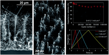
Micro-supercapacitors are increasingly foreseen as future energy storage or power buffer solutions for small scale integration on-chip. However, widely used electrode materials or electrolytes often proved to be incompatible with microelectronics processes. Although being the material of choice for on-chip integration, nanostructured silicon electrodes only recently caught attention for potential applications, and they displayed promising results especially for bottom-up silicon nanostructures, where the design liberty and fine control of nanostructure morphologies allow considerable improvements. The present work deals with the optimization of highly doped silicon nanowires (Si-NWs) and nanotrees (Si-NTrs) pioneered in the laboratory using an innovative, fast and efficient electroless gold deposition method in order to explore a wide variety of 3D architectures and their physicochemical properties. Through a systematic study of branches and trunks morphologies, the nature inspired nanotrees have been drastically improved compared to previously published works, resulting in excellent electrode properties, showing high energy and power densities, respectively, up to 2.8 mJ cm−2 and 235 mW cm−2. In addition, a cyclability of over a million charge–discharge galvanostatic cycles was determined using an enlarged electrochemical window of 4 V in an ionic liquid electrolyte.
In order to fulfill the requirements of such devices, micro-supercapacitors have recently attracted substantial attention1,2 owing to their high power and energy densities, their excellent cycling ability compared to batteries and the relatively simple scalability of the processes at extremely small scale (down to less than a square millimeter of geometric surface area).3 Among all materials, carbon4 stands in high grounds for pure double layer electrochemical capacitors, due to its simplicity of use, relative abundance and ease to achieve high specific capacitance. Several carbon based electrode materials display promising results for micro-supercapacitors applications, such as “onion like carbon”,3,5 activated carbon,3,6–8 carbon nanotubes,9,10 graphene materials,10–13 or carbide derived carbons.14 Pseudocapacitive compounds,15 for instance metal oxides (RuO2,16,17 MnO2…18–20) and nitrides (TiN,21 VN22,23) or conductive polymers (PEDOT and derivatives,24,25 PPy,26 PANi…27) have also been intensively investigated owing to their extremely large specific capacitance due to fast and reversible surface redox reactions.
However, most of the materials studied in the literature still present some inherent incompatibilities for integration on a regular electronic device. For example the high temperature solder reflow conditions used to attach devices on an electronic circuit (usually over 200 °C for several tens of seconds) would be problematic for most aqueous electrolytes used for pseudocapacitive oxide materials, or fragile carbonaceous materials. Advanced new materials thus need to be designed directly from the on-chip integration point of view.
Although ubiquitous in micro-electronics for decades, silicon only recently attracted attention as a potential material for “on chip” micro-supercapacitor integration. Despite having excellent thermal stability, evident “on chip” applicability and tunable electrical properties, only a handful of studies were conducted on this field. The main drawback of silicon consists in the extreme difficulty to tailor large surface area conductive silicon, since highly porous silicon remains extremely fragile and reactive. While achieving fairly stable large surface area conductive carbon leads to specific capacitances over 100 F g−1 with a good cycling stability, designing conductive porous silicon nanostructures with a sufficient surface area to exhibit interesting capacitances but also keep a good stability still represents a challenge. In addition, on-chip applications are rather limited in terms of geometric area occupied by the device, than by mass or volume of active material, thus the studied compounds should be compared by surface specific capacitances in F cm−2. This parameter explains why certain materials can be advantageous for micro-supercapacitor devices albeit delivering poor mass-specific capacitances.
In this context, two main methods can be employed in order to yield conductive 3D nanostructured silicon electrodes for supercapacitors: the top-down approach28 consisting principally in etching a conductive silicon substrate to yield porous silicon or etched Si-NWs and the bottom-up approach usually via Chemical Vapor Deposition (CVD) resulting in silicon nanostructures grown on a substrate (e.g. Si-NWs, Si-NTrs).
Top-down etching although simple and relatively inexpensive yields high surface area silicon nanostructures,29 that can be used in supercapacitors. Nonetheless, the fragility and lack of control on the electrical properties of the nanostructures often require a conformal coating in order to upgrade capacitance and cyclability, for instance with carbon,30 graphene,31 diamond,32 titanium nitride33 or silicon carbide34 with capacitance values up to 325 mF cm−2 for carbon sheath coated porous Si-NWs.35
On the other hand, bottom-up silicon nanostructures can be finely tuned in terms of morphology and electronic properties,36 with moderate to high surface enhancements compared to bulk silicon at the expense of a complex and pricy material synthesis process. Moreover, bottom-up approach permits a remarkable liberty in the design of innovative nanostructures, such as silicon-nanotrees, where the addition of branches to Si-NWs allows obtaining high surface area yet robust and conductive supported electrode materials. After the original work by Thissandier et al. on CVD Si-NWs as electrodes for supercapacitors,37 highly doped Si-NWs and Si-NTrs displayed unmatched characteristics using ionic liquid electrolytes (EMIM TFSI, PYR13 TFSI), with a 4 V electrochemical window,38,39 up to 225 mW cm−2 power densities, and more than 106 charge/discharge cycles without significant damages.40 Contrary to most top-down Si-nanostructures, these properties are obtained for uncoated pure Si-nanostructures, compatible with microelectronics fabrication processes and with capacitances up to 900 μF cm−2 in three electrodes cell setup reported for Si-NTrs.40
However, capacitance still needs to be further increased to reach interesting values for on chip integration.
In particular, CVD catalyst optimization has scarcely been explored in the literature, although it remains one of the simplest paths to change and improve the bottom-up nanostructures morphologies. Bottom-up silicon nanostructures are most frequently synthetized using colloid37 or thin film evaporation40 to deposit the gold catalyst. However, these techniques are expensive and non-selective, for instance gold evaporation require a high vacuum and usually deposits gold over the whole deposition chamber, thus consuming large quantities of precious metal. The non-selectivity can hinder on-chip applications, for instance if gold is unselectively deposited on microfabricated on-chip Si-NWs electrodes to produce Si-NTrs, it would require delicate patterning steps to remove the excess gold before the second CVD step. For these reasons this study uses an innovative, selective and time efficient electroless gold deposition method,41,42 for the first time in the field of bottom-up silicon supercapacitors to the best of our knowledge.
The aim of the present work is to design and optimize silicon nanowires and nanotrees using electroless gold deposition in order to explore the variety of morphologies and properties made possible by the bottom-up approach and to maximize the specific capacitance of such system. Among the endless possibilities offered by the CVD growth, this study will mainly focus on a two steps synthesis of Si-NTrs, with the aim of optimizing synergistically trunks and branches diameter, densities and lengths to increase the capacitive properties of the electrodes.
All electrochemical characterizations were performed in an argon filled glove box at room temperature in order to avoid any water or oxygen contamination. The electrolyte used in all measurement was 1-ethyl-3-methylimidazolium bis(trifluoromethylsulfonyl)imide (EMI-TFSI) ionic liquid purchased from Solvionic (France) with 99.5% purity (≤0.05% water and ≤0.001 ppm of halide content) and used without further purification.
Gold mass estimations were conducted by weighing several 1 cm2 samples at the same time on a Mettler Toledo AG245 balance with 0.01 mg readability, and by considering eqn (1) to calculate the quantity of gold deposited from the samples mass difference:
3Si + 18HF + 4AuCl4− → 3SiF62− + 4Au + 18H+ + 16Cl− | (1) |
The total mass of the optimized Si-NTrs grown on the sample was also calculated by the same scaling method, with a total mass of Si-NTrs approximating 1.2 μg cm−2 ± 0.2 μg cm−2.
Three electrodes cell measurements were conducted using a homemade Teflon cell connected to an Autolab PGSTAT302 potentiostat/galvanostat equipped with a FRA 2 module. The nanostructured electrode (active area 0.4 cm2) was used as the working electrode with a twisted platinum wire as the counter electrode and an Ag/Ag+ reference electrode (10 mM silver trifluoromethanesulfonate in EMI-TFSI). Each electrode was tested by cyclic voltammetry at different scan rates (between 50 mV s−1 and 10 V s−1) with a 4 V electrochemical windows. Impedance spectroscopy was also measured by applying 10 mV amplitude signals from 0.01 to 100000 Hz. The capacitance values from CV curves were measured after a few hundred CV cycles at 1 V s−1 to avoid any parasitic effects of surface oxide formation or ionic liquid impurities reactions.
Two electrodes cell measurements were performed by sandwiching a glass fiber paper separator soaked in EMI-TFSI between two symmetric nanostructured electrodes connected to a potentiostat/galvanostat (VMP3, Bio-logic, France). EIS (50 mV amplitude signal, 0.01 to 400000 Hz), cyclic voltammetry at different scan rates and galvanostatic charge/discharge cycling at different current densities were conducted. Areal capacitance values were calculated from CV and galvanostatic charge/discharge curves using respectively eqn (2) and (3):
![]() | (2) |
![]() | (3) |
![]() | (4) |
![]() | (5) |
![]() | (6) |
After this step, the obtained Si-NWs or trunks can be coated with a layer of gold catalyst and another CVD growth will lead to branches on the trunks, yielding a sample covered by a highly conductive silicon nanotrees forest.
The main interest of this nanostructuration is to obtain a large enhancement of the specific surface, which will lead to an increase in the capacitance of the electrode. In order to achieve the largest value of specific surface, the nanotrees should be optimized in regard to the densities, lengths and diameters of both trunks and branches.
This study also displays the fact that some parameters are interdependent, such as the density and the mean diameter of the Si-NWs, or the trunks diameters and the branches densities. For instance, increasing the diameter of the trunks can decrease their density, and thus reduce the overall specific surface of the Si-NWs electrode. However, large diameter trunks can also achieve higher branches densities, which can be in total more profitable than using higher density but lower diameter trunks.
In order to determine the best nanostructure morphology for supercapacitor applications, this study focuses on two main parameters highlighted in Fig. 1:
- The gold catalyst quantities which will affect both mean diameter and density of the Si-NWs or Si-NTrs’ branches. This step has been performed by using electroless gold deposition method.45
- The length of the trunks and branches which are solely depending on the CVD growth time with other parameters being kept similar.
All other parameters were kept similar during the production of the samples. Using this simple method, a systematic experimental study was conducted on several points: trunks diameters and density, branches diameters and densities on different trunks samples and finally branches lengths comprised between 5 and 70 μm. Nanostructured electrodes were designed by varying these parameters and were both studied in three and two electrodes cells configurations, using EMI-TFSI as the electrolyte as previously reported.38
![]() | (7) |
![]() | (8) |
This reaction can be extremely quick, thus reducing sample preparation time and is performed in water, at room temperature, with only a fraction of a milliliter of dilute AuCl4− solution consumed per sample. Moreover, the gold plating occurs only on silicon surfaces, facilitating patterning and on-chip integration of Si-NTrs. The gold quantity deposited can also be easily tailored by varying the plating bath concentration or deposition time, and yields relatively conformal gold layers even on complex geometries.
Consequently, the Si-NTrs synthesized in this study were grown using two electroless deposition steps with various concentrations to optimize the parameters described in the previous section. Three different concentrations of AuCl4− were used for these two steps, 10 mM, 2 mM and 1 mM respectively. The nanostructures yielded will be referred by the concentration used for each electroless steps, for instance 10 mM trunks will correspond to Si-NWs obtained by CVD of a sample coated by 10 mM electroless bath, and 2 mM/10 mM Si-NTrs will correspond to silicon nanotrees yielded by CVD of 2 mM trunks coated by 10 mM for branches.
In order to find the most suitable nanostructures for supercapacitors, three electrodes cell experiments were conducted. Fig. 2(g) displays the cyclic voltammetry curves of the different Si-NWs samples and n-doped bulk silicon at a scan rate of 1 V s−1 with a 4 V electrochemical window ([−2.5 V; 1.5 V] vs. Ag+/Ag). As reported previously, the silicon electrodes withstand this high voltage window with an almost ideal capacitive behavior.38 The capacitances values derived from CV curves exhibit a rather large enhancement between flat and nanostructured silicon, with values of 5, 180, 280 and 320 μF cm−2 for bulk silicon, 1, 2 and 10 mM, 50 μm long Si-NWs respectively. The capacitance thus increases with the gold quantity deposited prior to the growth, implying that for 50 μm long Si-NWs, large diameter trunks samples are developing a higher surface area compared to smaller diameter ones.
For 1 and 2 mM trunks, the gold deposition consist in a thin layer of crushed gold coated nanowires on top of a subjacent forest with almost no gold deposited in it. The thickness of the subjacent layer can vary depending on the location on the sample between 20 to 40 μm.
For all types of trunks, the quantity of gold deposited on the nanowires decreases with the AuCl4− concentration, without any fundamental changes in the morphology of the nanostructures or in the distribution of the gold deposit.
Fig. 3(e–h) illustrate the morphologies obtained from the samples displayed in Fig. 3(a–d) after a second CVD step on the gold coated Si-NWs, yielding branches with a maximum length of 20 μm. For large diameter 10 mM trunks, hyperbranched nanostructures were observed regardless of the second gold deposition concentrations, with tree like morphologies and several dozens of branches connected to each trunks and spreading in all directions. The maximum density of secondary growth wires occurs on top of the trunks, with the branches density, diameter and length decreasing with the distance from the tip to the base (Fig. 4(e)). Fig. 4(f) displays a schematic of Fig. 4(e) in order to clarify the complex features of the obtained Si-NTrs. This result is directly related to the gold distribution on the Si-NWs prior to growth with the progressive decrease of the gold quantity from the top to the bottom of the Si-NWs layer. A more detailed study of the branches diameter distribution can be found in the ESI Fig. S4.†
For 1 and 2 mM trunks, the morphologies obtained after the second growth are less prone to natural analogies, with a Si-NWs layer completely covering the subjacent crushed trunks layer. The nanostructures can be divided into a 3 layers stack with, from the substrate to the top: (i) a layer of crushed trunks, (ii) then a dense network of trunks and branches interpenetrated, corresponding to the layer of gold coated trunks previously described, where numerous branches growths were seeded, (iii) and finally on the top, freely grown branches. With this stack structure, top view SEM pictures of the samples only reveal a Si-NWs forest with no distinguishable features of nanotrees (Fig. S5†).
As for the gold deposition step, for each type of trunks, no clear morphological differences can be seen between the nanostructures with 10, 2 and 1 mM branches. The branches may present slightly smaller densities and diameters but the specific surface developed by the different samples cannot be clearly derived solely on the SEM pictures. Especially, the differences in densities and surface coverage of the branches cannot be quantitatively derived. Moreover, the analysis of the 3D interpenetrated Si-NWs network layer obtained with the 1 and 2 mM trunks, and its potentially accessible surface to ions for electrochemical capacitors remains a challenge.
In order to determine which nanostructure is the best for supercapacitor applications, the capacitance values of these nanostructured electrodes were assessed in three electrodes cell, yielding the results exhibited in Table 1. One clear result derived from these measurements is that, regardless of the trunks types, a higher quantity of gold deposited for branches generations yields a larger capacitance value. For 10, 2 and 1 mM trunks, the nanostructures generated with 10 mM branches largely surpasses in capacitance the values obtained with 2 mM which are slightly larger than the ones with 1 mM branches. More surprisingly, at equal branches types, the nanostructures with 10 mM and 2 mM trunks show marginally equal capacitance values, whereas their morphologies greatly differ. These values confirm that the 3D dense interpenetrated Si-NWs network of these samples can provide a significant accessible surface area for supercapacitor devices. However, even-though nanostructures with 1 mM trunks display the same kind of morphologies, capacitances values are significantly lower than for 2 mM trunks, stressing the fact that the balance between trunks' morphologies and branches generation remain complex.
Trunks only | 10 mM branches | 2 mM branches | 1 mM branches | |
---|---|---|---|---|
10 mM trunks | 320 | 1290 | 835 | 780 |
2 mM trunks | 280 | 1270 | 805 | 680 |
1 mM trunks | 180 | 980 | 540 | 505 |
The main outcome of this study is that nanostructures grown using 10 and 2 mM, 50 μm long trunks with 10 mM, 20 μm long branches yielded samples with three electrodes cell capacitance values of about 1.3 mF cm−2 which is more than 4 times the bare trunks samples capacitance values, and more than 250 times flat silicon capacitance values. Apart from the capacitance values, the electrochemical behaviour of the Si-NTrs is similar to the bare trunks behaviour, showing that the branches addition only enhanced the surface area without significantly changing the electrical characteristics of the electrodes or the properties of the electrode/electrolyte interface.
The three electrodes cell capacitances of nanotrees samples with different branches lengths are shown in Fig. 5(a). Strikingly, the capacitance value of the Si-NTrs with branches only 5 μm long almost doubles compared to the bare trunks samples, exhibiting the large increase of the surface area occurring upon the seeding of branches on the trunks. Moreover, after this large enhancement, the capacitance continuously increases with the length of the branches, with values from 800 μF cm−2 for 5 μm long branches Si-NTrs to more than 1700 μF cm−2 for 72 μm long branches Si-NTrs. This extremely high capacitance value remains unmatched to the best of our knowledge for bottom-up silicon based supercapacitive electrodes and represents a large improvement compared to the 900 μF cm−2 previously obtained for Si-NTrs electrodes.40 Fig. 5(b) displays the cyclic voltammetry of these Si-NTrs in regard with the corresponding bare trunks and the bulk silicon, exhibiting the large enhancement of the capacitive behaviour due to the nanostructure optimization.
Full characterization of the optimized Si-NTrs and of the corresponding trunks were conducted in three electrodes cell, as well as in two electrodes “sandwich” type symmetric device. The results of this study are pictured in Fig. 6. The three electrodes cell cyclic voltammetry curves at different scan rates materialize the remarkable capacitive properties of the nanostructured electrodes even at scan rates as high as 10 V s−1, Fig. 6(a). Capacitances values derived from these curves displayed in Fig. 6(b) highlight the retention of capacitance at higher scan rate with 900 μF cm−2 measured at 10 V s−1 compared to respectively 1.7 and 3.8 mF cm−2 at 1 and 0.1 V s−1.
Symmetric device measurements indicate a nearly ideal capacitive response with triangular shaped galvanostatic charge/discharge cycles at different current densities (Fig. 6(c)), with capacitances as high as 350 μF cm−2 from CV at 1 V s−1 as well as galvanostatic charge/discharge cycles at 1 mA cm−2. The capacitance fades from single electrode to a symmetric device of nearly a factor of 5, exceeding the theoretical value of 2. One possible explanation may be that the partial wetting of the electrodes by the ionic liquid contained in the soaked separator resulting in a decreased accessible surface area. Another explanation is that the pressure applied to the nanostructures during cell assembly crushes the nanostructures, although no clear evidence of mechanical modifications can be seen on tested electrodes. The cycling ability of the optimized Si-NTrs devices is displayed Fig. 6(d), with an excellent capacitance retention of 80% after one million galvanostatic cycles of charge/discharge (4 V, 1 mA cm−2), following the same cycling behaviour that previously reported Si-NWs supercapacitor devices.39,40 Electrochemical impedance spectroscopy (Fig. 6(e and f)) denotes an equivalent series resistance of 17 Ω and a relatively short characteristic time47 of 32 ms (−45° phase angle frequency of 31 Hz). These measurements lead to values of 235 mW cm−2 maximum power density, and energy densities ranging from 2.8 mJ cm−2 to 2.3 mJ cm−2 at power densities of respectively 2 mW cm−2 and 30 mW cm−2, which are extremely interesting values for typical micro-supercapacitor applications.
The same characterizations were conducted on the bare trunks and are displayed in ESI Fig. S6.†
Energy and power densities performances of the optimized trunks and Si-NTrs are plotted in Fig. 7, in addition to our first results in the field of Si-NWs based supercapacitors and other state-of-the-art results for purely double layer micro-supercapacitor. This Ragone plot clearly shows the tremendous improvements due to the nanostructures optimization, with final results for optimized Si-NTrs in the same order of magnitude than state of the art carbon based micro-supercapacitor devices.
Footnote |
† Electronic supplementary information (ESI) available: Diameter distributions for 10/2/1 mM trunks, SEM cross section of 10 mM/10 mM Si-NTrs with different branches lengths, SEM cross section and corresponding branches diameter distributions, SEM views of 2 mM/10 mM Si-NTrs before and after 2nd CVD and electrochemical characterization of 10 mM trunks. See DOI: 10.1039/c6ra14806a |
This journal is © The Royal Society of Chemistry 2016 |