DOI:
10.1039/C6RA14685F
(Paper)
RSC Adv., 2016,
6, 72286-72294
Thermoelectric properties of highly-mismatched alloys of GaNxAs1−x from first- to second-principles methods: energy conversion†
Received
6th June 2016
, Accepted 22nd July 2016
First published on 26th July 2016
Abstract
The transport properties of GaNxAs1−x (x = 0.0, 0.25, 0.5, 0.75 and 1.0) alloys are investigated using the semi-classical Boltzmann theory as implemented in the BoltzTraP code. The electronic structures are calculated using the full potential linearized augmented plane wave method within the recently modified Becke-Johnson potential to solve the exchange correlation potential. These alloys possess a direct band gap varying between 0.5 and 3.2 eV. The ‘special quasi-random structures’ approach of Zunger was used to reproduce the randomness of the GaNxAs1−x alloys for the first few shells around a given site. The carrier concentration (n), electrical conductivity (σ/τ), Seebeck coefficient (S), electronic thermal conductivity (κe/τ) and the electronic power factor (S2σ/τ), as a function of temperature were obtained for GaNxAs1−x alloys. In addition, the transport properties as a function of chemical potential at three constant temperatures were investigated. It has been found that GaNxAs1−x alloys show good transport properties, therefore, we expect that these alloys could be possible potential candidates for clean energy applications.
1. Introduction
Thermoelectric power generators can convert heat into electricity, which is a good alternative solution for energy and environment problems.1 Ever since this discovery, extensive studies were done on several materials to enhance their thermoelectric properties for technological applications.2–11 The development of novel thermoelectric materials has attracted a great deal of interest due to their significant potential applications ranging from clean energy to photon sensing devices. The efficient thermoelectric materials can be classified into three types: complex crystals, alloys and nano-crystals.12 They can provide a significant contribution to solve global sustainable energy problems. Thermoelectric materials play an important role in global sustainable energy solutions. These materials are not only used in generating electricity from waste heat but also used as solid-state Peltier coolers.12 In the complex crystals category there are ternary alloys such as GaNxAs1−x. These can be considered to be possible potential candidates for applications in optoelectronic, semiconductor lasers, and optical detectors.13–19 It was found that the electronic structure and optical properties of GaAs are modified significantly when a small concentration of N doped into GaAs. There is a significant increase in the band gap when As is replaced by N.20 It was reported that nitrogen in GaNAs perturbs the conduction bands and reduces electron mobility21–23 because nitrogen is highly electronegative (3.04) in addition to its small size, and it is attractive to electrons, in comparison to the size and the electronegativity of As (2.18).
Several workers have reported the influence of vary the content of N on the electronic properties of the doped alloys. Since the energy gap is in the range 0.5–1.5 eV, these alloys could have a potential application in thermoelectric devices. As a natural extension to our previous work on the electronic structure24 and the nonlinear optical properties of GaNxAs1−x alloys,25 we thought it would be interesting to study the transport properties of GaNxAs1−x alloys.
2. Computational method
The all electron full potential linearized augmented plan wave plus local orbital (FP − L(APW + lo)) method26 within density functional theory (DFT) and the semi-classical Boltzmann theory as implemented in the BoltzTraP code27 were used to calculate the transport properties of GaNxAs1−x alloys with x = 0.0, 0.25, 0.5, 0.75 and 1.0. The recently modified Becke-Johnson potential (mBJ)28 was used to solve the exchange correlation functional. In calculating the self-consistent band structure within DFT, both local-density approximation (LDA)29 and the generalized-gradient (GGA)30 usually underestimate the energy gap.31 This is mainly due to the fact that they have simple forms that are not sufficiently flexible to accurately reproduce both the exchange-correlation energy and its charge derivative. To overcome this drawback we proposed mBJ. The mBJ, a modified Becke-Johnson potential, allows the calculation of band gaps with accuracy similar to the very expensive GW calculations.28 It is a local approximation to an atomic “exact-exchange” potential and a screening term.
The number of basis functions were used up to RMTKmax = 7.0 (where RMT is the minimum radius of the muffin-tin spheres and Kmax gives the magnitude of the largest k vector in the plane wave expansion). The values of the sphere radii and Kmax are kept constant over all the range of lattice spacing. The Fourier expanded charge density was truncated at Gmax = 14 (Ryd)1/2. In order to reproduce the randomness of the alloys for the first few shells around a given site, the ‘special quasi-random structures’ (SQS) approach of Zunger et al.32 was used. We would like to mention here for the composition x = 0.25 and 0.75 the simplest structure is an eight-atom simple cubic lattice (luzonite): the cations with the lower concentration form a regular simple cubic lattice (see Fig. 1(b) and (d)). For x = 0.5 composition, the smallest ordered structure is (001) super-cell (see Fig. 1(c)). The muffin-tin radii for the composition x = 0.25 and 0.75 are 1.95, 1.9 and 1.6 atomic units (a.u.) for Ga, As and N respectively. For x = 0.5 the muffin-tin radii was set to be 2.14 a.u. for Ga, N and As. A mesh of 35 special k-points was used for ternary alloys except for the case of x = 0.5, where we used a mesh of 64 special k-points in the irreducible Brillouin zone (IBZ). For calculating the transport properties of GaNxAs1−x alloys a denser meshes of 50![[thin space (1/6-em)]](https://www.rsc.org/images/entities/char_2009.gif) 000 k-points in IBZ for the ternary alloys were used. The self-consistent calculations are converged since the total energy of the system is stable within 10−5 Ry.
000 k-points in IBZ for the ternary alloys were used. The self-consistent calculations are converged since the total energy of the system is stable within 10−5 Ry.
 |
| | Fig. 1 The structure of the unit cell of GaNxAs1−x (x = 0.0, 0.25, 0.5, 0.75 and 1.0) alloys; (b and d) the simplest structure is an eight-atom simple cubic lattice (luzonite): the cations with the lower concentration form a regular simple cubic lattice; (c) for x = 0.5 composition, the smallest ordered structure is (001) super-cell. | |
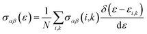
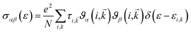
We have used the semi-classical Boltzmann theory as incorporated in BoltzTraP code27 to calculate the thermoelectric properties. The transport coefficients that based on rigid band approach to conductivity is given by;
| |
 | (1) |
| |
σαβ(i,![[k with combining right harpoon above (vector)]](https://www.rsc.org/images/entities/i_char_006b_20d1.gif) ) = e2τi,ϑα(i,)ϑβ(i,) ) = e2τi,ϑα(i,)ϑβ(i,)
| (2) |
| |
 | (3) |
where
e represent charge of electron,
τ is the relaxation time,
α and
β are the tensor indices,
N is the number of
k-points,
ϑα(
i,
) and
ϑβ(
i,
) are the group velocities. It is important to mention that in BoltzTraP code the relaxation time
τ taken as a constant.
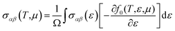
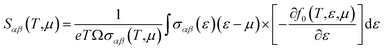
27 The transport coefficients can be written as a function of temperature and chemical potential
27,33 as follow;
| |
 | (4) |
| |
 | (5) |
| |
 | (6) |
where
Ω stands for volume of the unit cell, and
f0 is Fermi–Dirac distribution function. To gain high thermoelectric efficiency, it is important that the material possess high electrical conductivity, large Seebeck coefficient and low thermal conductivity.
34
Simulations of the transport properties is transition from first- to second-principles methods. The first-principles method used here is all-electron full potential linear augmented plane wave method whereas the second-principles is BoltzTraP code,27 which solves the semi-classical Bloch–Boltzmann transport equations.27 Transport properties were obtained from the ground state within the limits of Boltzmann theory35–37 and the constant relaxation time approximation as implemented in the BoltzTraP code.27 In short, BoltzTraP performs a Fourier expansion of the quantum chemical band energies. This allows to obtain the electronic group velocity and inverse mass tensor, as the first and second derivatives of the bands with respect to k. Applying the electronic group velocity and inverse mass tensor to the semiclassical Boltzmann equations, the transport tensors can be evaluated.
3. Results and discussion
3.1. Salient features of the electronic band structures
Since the electronic band structures are very important for calculating the effective mass and the transport properties, therefore we will recall the main features of the electronic band structure of GaNxAs1−x (x = 0.0, 0.25, 0.50, 0.75 and 1.0) alloys.24 Fig. 2(a–e) shows the electronic band structure along the high symmetry points of the first Brillouin zone. We set the zero-point of energy (Fermi level) at the valence band maximum (VBM). The VBM and the conduction band minimum (CBM) were located at the center (Γ) of first Brillouin zone, resulting in a direct band gap of about 1.51, 0.50, 0.91, 1.43 and 3.0 eV for GaAs, GaN0.25As0.75, GaN0.5As0.5, GaN0.75As0.25 and GaN respectively. The calculated values of the energy band gap of the ternary alloys and their parent are compared with the previous theoretical results24 and the experimental data38–47 as shown in Table 1. We can see that for the ternary alloys (GaN0.25As0.75, GaN0.5As0.5, GaN0.75As0.25) increasing the content of N cause to shift the CBM towards higher energies resulting in significant increase in the band gap values. The increase in band gap due to N is thought to be due to a resonant interaction between the N-2s state and the bottom of the conduction band.46,48 It was reported that there is a large increasing in the band gap even by replacing just one percent of the As by N.20 This blue shift is characterized by the optical bowing parameter which reaches 18–20 eV for nitrogen concentration less than 5.0%, which is about an order of magnitude larger than other III–V ternary alloys that exhibit a bowing of about 1.0 eV.49–51
 |
| | Fig. 2 The calculated electronic band stature of GaNxAs1−x (x = 0.0, 0.25, 0.5, 0.75 and 1.0) alloys, using mBJ. | |
Table 1 Calculated energy band gap (Eg in eV) in comparison with the previous theoretical results and the experimental data of the GaNxAs1−x (x = 0.0, 0.25, 0.5, 0.75 and 1.0) alloys
| Compounds |
Eg (this work) |
Eg (previous work) |
Eg (experiment) |
| Ref. 24. Ref. 38. Ref. 39. Ref. 40. Ref. 41 and 42. Ref. 43. Ref. 44. Ref. 45. Ref. 46 at 0 K. Ref. 47 at 0 K. |
| GaAs |
1.51 |
0.46a, 0.14a, 0.62a |
1.42b, 1.63c, 1.52i, 1.51j |
| GaN0.25As0.75 |
0.50 |
0.0a, 0.0a, 0.38a |
|
| GaN0.5As0.5 |
0.91 |
0.33a, 0.16a, 0.65a |
|
| GaN0.75As0.25 |
1.43 |
1.00a, 0.66a, 1.18a |
|
| GaN |
3.0 |
1.89a, 1.51b, 2.04a |
3.38d, 3.1d, 3.2d, 1.48e, 2.08f, 2.65g, 2.00h |
Let us recall the main features of the calculated density of states of GaNxAs1−x (x = 0.0, 0.25, 0.50, 0.75 and 1.0) alloys,24 we noticed that replacing As atoms by N atoms cause significant influence in the density of states (See Fig. S1 ESI†) and the charge density near the density peaks is substantially attracted toward N atoms due to their high electronegativity.52 It has been found that24 the covalent bonding are more dominant in GaNxAs1−x alloys. Covalent bonding is more favorable for the transport of the carriers than ionic one.53 Also, due to the electro-negativity differences between Ga, As and N atoms, some valence electrons are transferred towards N atoms indicating the maximum charge accumulated around N atoms therefore, replacing As by N lead to enhance the transport properties.
3.2. Effective mass
Following Fig. 2(a–e), it is quite clear that the bands in the vicinity of Fermi level (EF) are parabolic, this would imply low effective mass for the carriers belonging to these bands and hence a high mobility. However, presence of carriers with large mobility is required for obtaining a higher electrical conductivity (σ). The thermoelectric power factor (S2σ/τ) is indirectly related to the effective mass through σ = neη and η = eτ/me,54 here we call the mobility as η in order to distinguish between the mobility and chemical potential (μ). The main factors to determine the transport properties are the effective charge-carrier's mass, the Seebeck coefficient and electrical conductivity of materials. The electron mobility characterizes how quickly an electron can move through a metal or semiconductor.
The calculation of the effective mass is used to simplify the band structure by making a similarity to the performance of a free element with that mass, it can be considered as simple constant of a material. The effective mass provides a significant basic parameter that leverages discernable properties of a solid, encompassing everything from the efficiency of a solar cell to the pace of an integrated circuit. We have calculated the effective mass of electrons  from the band structure of the GaNxAs1−x alloys with N-concentration 0.0, 0.25, 0.5, 0.75 and 1.0. Usually we estimated the value of the effective mass from the conduction band minimum curvature. The diagonal elements of the effective mass tensor for the electrons in the conduction band are calculated following this expression;
| |
 | (7) |
The effective mass of electron is assessed by fitting the electronic band structure to a parabolic function eqn (7). We have calculated the electron effective mass ratio  , effective mass ratio of the heavy holes
  and light holes
  , around Γ point the center of the BZ for GaNxAs1−x (x = 0.0, 0.25, 0.5, 0.75 and 1.0) alloys. These values are listed in Table 2. It is clear that the effective mass ratio increases with moving from GaAs → GaN0.25As0.75 → GaN0.5As0.5 → GaN0.75As0.25 → GaN.
Table 2 The calculated electron effective mass ratio  , effective mass of the heavy holes
  and light holes
  , around Γ point the center of the BZ for GaNxAs1−x (x = 0.0, 0.25, 0.5, 0.75, 1.0) alloys
| Effective mass ratio |
GaAs |
GaN0.25As0.75 |
GaN0.50As0.50 |
GaN0.75As0.25 |
GaN |
 |
0.0012 |
0.0018 |
0.0026 |
0.0027 |
0.0046 |
 |
0.0124 |
0.0168 |
0.0187 |
0.0215 |
0.0256 |
 |
0.0012 |
0.0015 |
0.0022 |
0.0030 |
0.0034 |
3.3. Transport properties
The semi-classical Boltzmann theory as implemented in the BoltzTraP code27 was used to calculate the electronic transport properties of the thermoelectric materials with a constant relaxation time τ.27,55–57 It has been proven that the BoltzTraP code is a very efficient technique for obtaining the electronic transport properties of the thermoelectric materials.27,55–57 The carrier concentration (n), electrical conductivity (σ/τ), Seebeck coefficient (S), electronic thermal conductivity (κe/τ) and the electronic power factor (S2σ/τ) as a function of temperature were obtained for GaNxAs1−x alloys with x = 0.0, 0.25, 0.5, 0.75 and 1.0 in the temperature range 50–800 K.
Better thermoelectric properties are determined by a combination of high mobility and reasonable carrier's concentration. In Fig. 3(a) we have illustrated the carrier's concentration (n) of GaNxAs1−x alloys as a function of temperature. We can see that for x = 0.25, 0.5, 0.75 the carrier's concentration increases exponentially with increasing the temperature whereas for the parent alloys there is insignificant increase in the carrier's concentration with increasing the temperature. As a remarkable finding we observed that GaN0.25As0.75 and GaN0.75As0.25 exhibit the same value of n of about (0.008 e per uc) at 100 K, while GaN0.5As0.5 exhibits a lower value of about 0.004 e per uc at 100 K. The carrier concentration shows a maximum value at 800 K of about 0.058 e per uc for GaN0.75As0.25, whereas it is 0.049 and 0.047 e per uc for GaN0.25As0.75 and GaN0.5As0.5. In these ternary alloys there are three types of atoms with different concentrations and different electro-negativity. According to Pauling scale the electro-negativity of N, As and Ga atoms are 3.04, 2.18 and 1.81, respectively. Therefore, the electro-negativity difference will be bigger between the atoms leading to more charge carrier concentrated around the atom which exhibits higher electro-negativity i.e. N atom. This may could explain why GaN0.75As0.25 exhibits the highest n among the others in the temperature range. The carrier mobility as a function of carrier's concentration for GaNxAs1−x (x = 0.0, 0.25, 0.5, 0.75 and 1.0) is illustrated in Fig. 3(b) and (c). It is clear that the carrier's mobility decreases with increasing the carrier's concentration due to increasing the scattering rate. We have compared our results with the previous experimental data for GaAs58–60 good agreement was found (See Fig. S2a and b ESI†). It has been found that increasing the content of N leads to reduce the mobility due to increase the scattering rate which is attributed to relatively small radius and the high electro-negativity of N compare to As that it replaces.61
 |
| | Fig. 3 (a) The temperature induced carrier concentration per unit cell (e per uc) versus temperature; (b) calculated carrier's mobility vs. carrier's concentration of GaNxAs1−x (x = 0.25, 0.5, 0.75) alloys; (c) calculated carrier's mobility vs. carrier's concentration of GaNxAs1−x (x = 0.0 and 1.0) alloys. | |
The electronic electrical conductivity (σ = neη) is related to the density of charge carriers (n) and their mobility (η = eτ/me). The temperature dependent electrical conductivity (σ/τ) was calculated at a certain value of chemical potential (μ = EF) as illustrated in Fig. 4(a). It is clear that σ/τ for GaNxAs1−x alloys increases with increasing temperature and GaN0.75As0.25 show the highest σ/τ in concordance with our observation from Fig. 3(a). The rapid increase in σ/τ with increasing the temperature is due to enhancing the charge carrier's concentration and the mobility of the electrons in the conduction band of these alloys. Further, we have calculated the electrical conductivity as a function of chemical potential (μ − EF = ±0.2 eV) at three constant temperatures (300, 600 and 900) K as shown in Fig. 4(b–f). It is clear that vary N cause significant enhancement in the electronic electrical conductivity due to the small size and the high electronegativity of N.
 |
| | Fig. 4 (a) Calculated electrical conductivity vs. temperatures; (b–f) the electrical conductivity as a function of chemical potential (μ − EF = ±0.2 eV) at three constant temperatures (300, 600 and 900) K. | |
The electronic thermal conductivity (κe/τ) can be estimated from the electrical conductivity σ using Wiedemann–Franz law. In Fig. 5(a) we have plotted the electronic thermal conductivity as a function of temperature for GaAs, GaN0.25As0.75, GaN0.5As0.5, GaN0.75As0.25 and GaN alloys at a certain value of chemical potential (μ = EF). We observed that the electronic thermal conductivity increases exponentially with increasing the temperature. It is clear that with increasing the temperature GaN0.75As0.25 and GaN alloys show the highest κe/τ among the others. Therefore, at the μ = EF increasing the temperature cause significant increases in the carrier's concentration and hence reduce the carrier's mobility due to increase the vibrations which lead to increase the scattering rate. The thermal conductivity has contributions from the lattice and electrons. BoltzTraP calculates only the electronic part.27 To ascertain that the temperature has significant influence on the electronic thermal conductivity of the investigated alloys, the electronic thermal conductivity was calculated as a function of chemical potential (μ − EF = ±0.2 eV) at three constant temperatures (300, 600 and 900) K as shown in Fig. 5(b–f). It has been noticed that increasing the temperature lead to significant increase in κe/τ. Therefore, following Fig. 5(b–f), 300 K is expected to be the optimal temperature to obtain lower κe/τ. To gain high thermoelectric efficiency, it is necessary that the material possess high electrical conductivity, large Seebeck coefficient and low thermal conductivity.34
 |
| | Fig. 5 (a) The electronic thermal conductivity versus temperature; (b–f) the electrical conductivity as a function of chemical potential (μ − EF = ±0.2 eV) at three constant temperatures (300, 600 and 900) K. | |
Fig. 6(a) illustrated the Seebeck coefficient (S) as a function of temperature. At low temperature (∼50 K) the Seebeck coefficient for GaAs is about 230 μV K−1 whereas for GaN its about 221 μV K−1 which show shallow influence with increasing the temperature. While for the ternary alloys at low temperature (100–300 K) the Seebeck coefficient increases rapidly with increasing the temperature. Then above 300 K the Seebeck coefficient exhibits saturated values. Among the ternary alloys GaN0.5As0.5 shows the highest value of S along the entire temperature range. That is attributed to the fact that increasing the temperature causes to enhance the hole doping in GaN0.5As0.5 alloy more than that in GaN0.75As0.25 and GaN0.25As0.75 alloys. Following Fig. 6(a) one can see that the Seebeck coefficient is positive over the entire temperature range, which implies that at a certain value of chemical potential (μ = EF) the GaNxAs1−x (x = 0.0, 0.25, 0.5, 0.75 and 1.0) alloys represent only p-type conductions. We have compared our calculated S of GaNxAs1−x (x = 0.0, 0.25, 0.5, 0.75 and 1.0) alloys to the measured and calculated S for GaAs58 as shown in Fig. S3 ESI.† It has been found that the increase in the calculated S for GaNxAs1−x (x = 0.0, 0.25, 0.5, 0.75 and 1.0) with increasing the temperature is consistent with previously measured and calculated S of GaAs58 (Fig. S3 ESI†). The Seebeck coefficient as a function of chemical potential at three constant temperatures (300, 600 and 900) K were calculated and presented in Fig. 6(b–f). It has been found that GaN exhibits largest Seebeck coefficient while GaN0.25As0.75 show the smallest Seebeck coefficient that is attributed to the fact that replacing 0.25 of As (radii = 115 pm) by N (radii = 65 pm) lead to increase the carrier's mobility and hence the scattering rate.
 |
| | Fig. 6 (a) The Seebeck coefficient versus temperature; (b–f) the Seebeck coefficient as a function of chemical potential (μ − EF = ±0.2 eV) at three constant temperatures (300, 600 and 900) K. | |
Fig. 7(a) show the electronic power factor (S2σ/τ) verses the temperature at a certain value of chemical potential. The power factor is a keynote quantity for measuring transport properties. Following Fig. 7(a), we can see that the power factor rapidly increases with increasing the temperature. It has been noticed that GaN0.75As0.25 and GaN alloys show the highest power factor among the others. That is attributed to the high content of N in GaN0.75As0.25 and GaN alloys due to the high electronegativity and small radii of N therefore, as the N content reduce the alloys exhibit low power factor. It is clear that the power factor decreases from GaN0.5As0.5 > GaN0.25As0.75 > GaAs. Furthermore, the electronic power factor is calculated as a function of chemical potential at three constant temperatures (300, 600 and 900) K as shown in Fig. 7(b–f).
 |
| | Fig. 7 (a) The power factor versus temperature; (b–f) the power factor as a function of chemical potential (μ − EF = ±0.2 eV) at three constant temperatures (300, 600 and 900) K. | |
4. Conclusions
We have investigated the transport properties of the GaNxAs1−x (x = 0.0, 0.25, 0.5, 0.75 and 1.0) alloys, by employing the semi-classical Boltzmann theory as implemented in the BoltzTraP code. Zunger approach (SQS) was used to generate the structures of the GaNxAs1−x alloys. The valence band gap maximum and the conduction band gap minimum are situated at Γ point the center of Brillouin zone resulting in a direct band gap. We have calculated the electron, heavy holes and light holes effective masses for GaNxAs1−x (x = 0.0, 0.25, 0.5, 0.75 and 1.0) alloys. Using the BoltzTraP code the carrier concentration (n), electrical conductivity (σ/τ), Seebeck coefficient (S), electronic thermal conductivity (κe/τ) and the electronic power factor (S2σ/τ) as a function of temperature at a certain chemical potential, also as a function of chemical potential at three constant temperatures were obtained for GaNxAs1−x alloys. Our calculations show that these alloys could be a possible potential candidate for thermoelectric energy conversion.
Acknowledgements
The result was developed within the CENTEM project, reg. no. CZ.1.05/2.1.00/03.0088, co funded by the ERDF as part of the Ministry of Education, Youth and Sports OP RDI programme and, in the follow-up sustainability stage, supported through CENTEM PLUS (LO1402) by financial means from the Ministry of Education, Youth and Sports under the National Sustainability Programme I. Computational resources were provided by MetaCentrum (LM2010005) and CERIT-SC (CZ.1.05/3.2.00/08.0144) infrastructures.
References
- H. Wang, W. Chu and H. Jin, Comput. Mater. Sci., 2012, 60, 224 CrossRef CAS.
- K. P. Ong, D. J. Singh and P. Wu, Phys. Rev. B: Condens. Matter Mater. Phys., 2011, 83, 115110 CrossRef.
- D. Parker and D. J. Singh, Phys. Rev. B: Condens. Matter Mater. Phys., 2011, 83, 233206 CrossRef.
- D. Parker, M. Du and D. J. Singh, Phys. Rev. B: Condens. Matter Mater. Phys., 2011, 83, 245111 CrossRef.
- D. J. Singh, Phys. Rev. B: Condens. Matter Mater. Phys., 2010, 81, 195217 CrossRef.
- K. P. Ong, D. J. Singh and P. Wu, Phys. Rev. Lett., 2010, 104, 176601 CrossRef PubMed.
- G. B. Wilson-Short, D. J. Singh, M. Fornari and M. Suewattana, Phys. Rev. B: Condens. Matter Mater. Phys., 2007, 75, 035121 CrossRef.
- D. J. Singh and D. Kasinathan, J. Electron. Mater., 2007, 36, 736 CrossRef CAS.
- D. J. Singh, Phys. Rev. B: Condens. Matter Mater. Phys., 2007, 76, 085110 CrossRef.
- D. J. Singh, Oxide Thermoelectrics, MRS Symp. Proc, 2008, vol. 1044, pp. U02–U05 Search PubMed.
- D. J. Singh, Alkaline earth filled nickel skutterudite antimonide thermoelectrics, US Pat., 8,487,178, 2013.
- H. A. R. Aliabad, M. Ghazanfari, I. Ahmad and M. A. Saeed, Comput. Mater. Sci., 2012, 65, 509 CrossRef.
- J. W. Orton and C. T. Foxon, Rep. Prog. Phys., 1998, 61, 1 CrossRef CAS.
- S. C. Jain, M. Willander, J. Narayan and R. V. Overstraeten, J. Appl. Phys., 2000, 87, 965 CrossRef CAS.
- I. Vurgaftman and J. R. Meyer, J. Appl. Phys., 2003, 94, 3675 CrossRef CAS.
- H. P. Xin and C. W. Tu, Appl. Phys. Lett., 1998, 72, 2442 CrossRef CAS.
- W. Shan, W. Walukiewicz, J. W. Ager III, E. E. Haller, J. F. Geisz, D. J. Friedman, J. M. Olson and S. R. Kurtz, Phys. Rev. Lett., 1999, 82, 1221 CrossRef CAS.
- M. Kondow, K. Uomi, A. Niwa, T. Kitatani, S. Watahiki and Y. Yazawa, Jpn. J. Appl. Phys., 1996, 35, 1273 CrossRef CAS.
- M. Bissiri, V. Gaspari, A. Polimeni, G. B. H. von Hogersthal, M. Capizzi and A. Frova, Appl. Phys. Lett., 2001, 79, 2585 CrossRef CAS.
- M. Weyers, M. Sato and H. Ando, Jpn. J. Appl. Phys., 1992, 31, L853 CrossRef CAS.
- W. Shan, W. Walukiwiecz, J. W. Ager, E. E. Haller, J. F. Geisz, D. J. Fiedman, J. M. Olson and S. R. Kurtz, Phys. Rev. Lett., 1999, 82, 1221 CrossRef CAS.
- S. Fahy and E. P. O'Reilly, Appl. Phys. Lett., 2003, 83, 3731 CrossRef CAS.
- A. Lindsay, E. P. O'Reilly, A. D. Andreev and T. Ashley, Phys. Rev. B: Condens. Matter Mater. Phys., 2008, 77, 165205 CrossRef.
- H. Baaziz, Z. Charifi, A. H. Reshak, B. Hamad and Y. Al-Douri, Appl. Phys. A: Mater. Sci. Process., 2012, 106, 687 CrossRef CAS.
- A. H. Reshak, J. Alloys Compd., 2014, 589, 213 CrossRef CAS.
- P. Blaha, K. Schwarz, G. K. H. Madsen, D. Kvasnicka and J. Luitz, Wien2k, An Augmented Plane Wave Plus Local Orbitals Program for Crystal Properties, Vienna University of Technology, Vienna, Austria, 2001 Search PubMed.
- G. K. H. Madsen and D. J. Singh, Comput. Phys. Commun., 2006, 175, 67 CrossRef CAS.
- F. Tran and P. Blaha, Phys. Rev. Lett., 2009, 102, 226401 CrossRef PubMed.
- W. Kohn and L. J. Sham, Phys. Rev. A, 1965, 140, 1133 CrossRef.
- J. P. Perdew, S. Burke and M. Ernzerhof, Phys. Rev. Lett., 1996, 77, 3865 CrossRef CAS PubMed.
- P. Dufek, P. Blaha and K. Schwarz, Phys. Rev. B: Condens. Matter Mater. Phys., 1994, 50, 7279 CrossRef CAS.
- A. Zunger, S.-H. Wei, L. G. Feireira and J. E. Bernard, Phys. Rev. Lett., 1990, 65, 353 CrossRef CAS PubMed.
- T. J. Scheidemantel, C. Ambrosch-Draxl, T. Thonhauser, J. V. Badding and J. O. Sofo, Phys. Rev. B: Condens. Matter Mater. Phys., 2003, 68, 125210 CrossRef.
- G. J. Snyder and E. S. Toberer, Nat. Mater., 2008, 7, 105–114 CrossRef CAS PubMed.
- P. B. Allen, in Quantum Theory of Real Materials, ed. J. R. Chelikowsky and S. G. Louie, Kluwer, Boston, 1996, pp. 219–250 Search PubMed.
- J. M. Ziman, Electrons and Phonons, Clarendon, Oxford, 2001 Search PubMed.
- C. M. Hurd, The Hall Effect in Metals and Alloys, Plenum, New York, 1972 Search PubMed.
- D. E. Aspnes, C. G. Olson and D. W. Lynch, Phys. Rev. Lett., 1976, 37, 766 CrossRef CAS.
- T. C. Chiang, J. A. Knapp, M. Aaono and D. E. Eastman, Phys. Rev. B: Condens. Matter Mater. Phys., 1980, 21, 3513 CrossRef CAS.
- W. J. Fan, M. F. Li, T. C. Chong and X. B. Xia, J. Appl. Phys., 1996, 79, 188 CrossRef CAS.
- P. E. Van Camp, V. F. Van Doren and J. T. Devreese, Phys. Rev. B: Condens. Matter Mater. Phys., 1991, 44, 9056 CrossRef CAS.
- P. E. Van Camp, V. F. Van Doren and J. T. Devreese, Solid State Commun., 1992, 81, 23 CrossRef CAS.
- B. J. Min, C. T. Chan and K. M. Ho, Phys. Rev. B: Condens. Matter Mater. Phys., 1992, 45, 1159 CrossRef CAS.
- M. Palumno, C. M. Bertoni, L. Reining and F. Finochi, Phys. B, 1993, 185, 404 CrossRef.
- V. Fiorentini, M. Methfessel and M. Scheffler, Phys. Rev. B: Condens. Matter Mater. Phys., 1993, 47, 13353 CrossRef CAS.
- For a review on the subject, see for instance, I. Vurgaftman, J. R. Meyer and L. R. Ram-Mohan, J. Appl. Phys., 2001, 89, 5815 CrossRef CAS.
- R. Roucka, J. Tolle, B. Forrest, J. Kouvetakis, V. R. D'Costa and J. Menéndez, J. Appl. Phys., 2007, 101, 013518 CrossRef.
- A. H. Reshak, H. Kamarudin, S. Auluck and I. V. Kityk, J. Solid State Chem., 2012, 186, 47–53 CrossRef CAS.
- M. Kondow, K. Uomi, K. Hosomi and T. Mozume, Jpn. J. Appl. Phys., 1994, 33, L1056 CAS.
- S. Sakai, Y. Ueta and Y. Terauchi, Jpn. J. Appl. Phys., Part 1, 1993, 32, 4413 CrossRef CAS.
- Y. Chen, J. Xi, D. O. Dumcenco, Z. Liu, K. Suenaga, D. Wang, Z. Shuai, Y.-S. Huang and L. Xie, ACS Nano., 2013, 7, 4610 CrossRef CAS PubMed.
- J. H. Lee, G. Wu and J. C. Grossman, Phys. Rev. Lett., 2010, 104, 016602 CrossRef PubMed.
- F. Wu, H. Z. Song, J. F. Jia and X. Hu, Prog. Nat. Sci., 2013, 23, 408–412 CrossRef.
- W. Shi, J. Chen, J. Xi, D. Wang and Z. Shuai, Chem. Mater., 2014, 26, 2669 CrossRef CAS.
- A. H. Reshak, S. A. Khan and S. Auluck, J. Mater. Chem. C, 2014, 2, 2346 RSC.
- A. H. Reshak and S. A. Khan, J. Magn. Magn. Mater., 2014, 354, 216–221 CrossRef CAS.
- A. H. Reshak, J. Chyský and S. Azam, Int. J. Electrochem. Sci., 2014, 9, 460–477 Search PubMed.
- https://escholarship.org/uc/item/2h7846vd.pdf.
- G. Homm, P. J. Klar, J. Teubert and W. Heimbrodt, Appl. Phys. Lett., 2008, 93, 042107 CrossRef.
- D. L. Rode and S. Knight, Phys. Rev. B: Solid State, 1971, 3, 2534 CrossRef.
- M. P. Vaughan and B. K. Ridley, The hall mobility in dilute nitrides, in Dilute III–V Nitride Semiconductors and Material Systems of Springer Series in Materials Science, ed. A. Erol, Springer Berlin Heidelberg, 2008, vol. 105, pp. 255–281 Search PubMed.
Footnote |
| † Electronic supplementary information (ESI) available. See DOI: 10.1039/c6ra14685f |
|
| This journal is © The Royal Society of Chemistry 2016 |
Click here to see how this site uses Cookies. View our privacy policy here. 
 *ab
*ab


 from the band structure of the GaNxAs1−x alloys with N-concentration 0.0, 0.25, 0.5, 0.75 and 1.0. Usually we estimated the value of the effective mass from the conduction band minimum curvature. The diagonal elements of the effective mass tensor for the electrons in the conduction band are calculated following this expression;
 , effective mass ratio of the heavy holes
  and light holes
  , around Γ point the center of the BZ for GaNxAs1−x (x = 0.0, 0.25, 0.5, 0.75 and 1.0) alloys. These values are listed in Table 2. It is clear that the effective mass ratio increases with moving from GaAs → GaN0.25As0.75 → GaN0.5As0.5 → GaN0.75As0.25 → GaN.
 , effective mass of the heavy holes
  and light holes
  , around Γ point the center of the BZ for GaNxAs1−x (x = 0.0, 0.25, 0.5, 0.75, 1.0) alloys


