
Control of consistent ordering in π-conjugated polymer films for organic field-effect transistor applications†
Mingyuan Pei‡
a,
Kwang Hun Park‡b,
Mi Janga,
Sang Bong Leec,
Joongyu Ahna,
Yun-Hi Kim*c and
Hoichang Yang*a
aDepartment of Applied Organic Materials Engineering, Inha University, Incheon 22212, Korea. E-mail: hcyang@inha.ac.kr
bDepartment of Polymer Science and Engineering, Gyeongsang National University, Jinju 52828, Korea
cDepartment of Chemistry, Gyeongsang National University, Research Institute of Nature Science (RINS), Jinju 52828, Korea. E-mail: ykim@gnu.ac.kr
First published on 22nd July 2016
Abstract
A novel conjugated copolymer, pDPP-(TV)2B-2DO, including donor (D) and acceptor (A) blocks of (TV)2B-2DO, 1,4-bis((E)-2-(thiophen-2-yl)vinyl)benzene with dodecyloxy moieties and diketopyrrolopyrrole (DPP) derivatives, respectively, was synthesized by Stille-coupling polymerization. The 60 kDa pDPP-(TV)2B-2DO showed good solubility in organic solvents and strong molecular interaction during film procedures. Semiconducting thin films were spun-cast on polymer-treated SiO2 from chloroform and annealed at temperatures ranging from 150 to 300 °C for 1 h. The electrical properties of these films in organic field-effect transistors (OFETs) were evaluated and correlated with π-conjugated ordering of the pDPP-(TV)2B-2DO, before and after annealing. Featureless aggregates of the face-on copolymer by the bulky B-2DO in the D block were dominant in the as-spun film and transformed into ordered rods or fibrils containing highly ordered edge-on polymers on the substrates after annealing. In terms of π-conjugated ordering, the as-spun and 250 °C-annealed pDPP-(TV)2B-2DO films contained highly-consistent chains with face-on and edge-on structures, respectively. The resulting OFETs yielded similar field-effect mobilities of 0.07 and 0.08 cm2 V−1 s−1, respectively, as well as on–off current ratios greater than 106 and a threshold voltage near 0 V. Therefore, the π-overlap of edge-on semiconducting polymers on gate dielectrics was not necessary to enhance the electrical performance of OFETs, but the high consistency in chain ordering was very important.
Introduction
Organic semiconductors have been considered as core materials for light-weight, low-cost, flexible electronics based on solution-processed organic field-effect transistors (OFETs) and organic photovoltaics (OPVs).1–8 It is well known that the control of intra- and inter-molecular interactions of π-conjugated organic semiconductors is a critical factor to achieve high performance devices.9–11Conjugated copolymers, based on the alternation of rigid and coplanar donor (D) and acceptor (A) blocks, have been recently synthesized because their rigid and coplanar chain conformations enhance charge transport and energy harvesting capabilities,10,12,13 compared to single conjugated systems, such as poly(3-hexyl thiophene) (P3HT),11 poly(3,3′′′-didodecyl quarterthiophene) (PQT-12),14 poly(2,5-bis(3-tetradecylthiophen-2-yl) thieno[3,2-b] thiophene) (pBTTT-C14).15 Recently, a diketopyrrolopyrrole (DPP) derivative has emerged as a promising A block segment to form long-range conjugated structures with various D blocks, yielding overall chain planarity and strong intermolecular ordering.9,16,17 Additionally, the DPP derivatives have excellent advantages in their good thermal stability, mechanical properties, and solution processability.17
DPP-based D–A copolymer thin films yielded high field-effect mobilities (μFET) greater than 1 cm2 V−1 s−1, encompassing small molecular systems.9,18 For example, Jang et al. reported that a D–A semiconducting copolymer, including DPP and thiophene-vinylene-thiophene (TVT) derivatives, could develop an extraordinary conducting layer in solution-processed and annealed films, yielding a μFET up to 3.7 cm2 V−1 s−1.9 Additionally, it was reported that a slightly different side-substituent DPP based copolymer yielded a high performance OFET with a μFET of approximately 4.3 cm2 V−1 s−1.19
A promising approach to realizing high performance polymer-based electronics is to synthesize semiconducting polymers, based on the understanding of the chemical structure-dependent variations of the conjugated D–A copolymers in the molecular π-orbital overlap, chain conformation, and ordering. It is important to properly control the chain ordering in both solutions and solid states. Inside an organic active channel, the charge carrier transport significantly depends on the conjugated orderings of the intra-, inter-molecules, and inter-grains, which can include different chain orientations with respect to the dielectric surface.20 It has been known that there exist distinct π-overlap directions of the organic semiconductors in these solid films, originating from the lateral and vertical π-overlaps of the edge- and face-on chains on the substrate, respectively. The charge carriers are mostly transferred along the conjugated and inter-molecular π-overlap planes, for which the conjugated backbones are required to orient along the preferential direction with respect to the substrate, yielding high electrical properties in the OFETs.21
In general, a fully-extended chain conformation is beneficial for forming a better π-overlap structure of conjugated polymers.11 In OFETs, also, a laterally-extended π–π stacking of edge-on chains on gate dielectrics favors charge-carrier transport along the S/D electrodes, while a vertical π-plane stacking of face-on chains is expected to induce the preferred charge-carrier separation in OPVs with vertically-aligned electrodes.22 Recently, Kim et al. reported that the balance between edge-on and face-on chain conformations of a rigid-like naphthalene diimide (NDI)-based copolymer in cast films could considerably improve the electrical properties of the resulting OFETs.23 The NDI-based OFETs showed a high μFET of 1.0 cm2 V−1 s−1, although the corresponding films contained a much higher portion of face-on chains with a π-overlap stacking normal to the S–D direction. However, it is still unclear how much the π-overlap ordering affects the electrical properties of polymeric semiconductors in organic electronics.
Here, we investigated the chain conformation and ordering effects of a D–A conjugated copolymer on the structural morphologies and electrical properties in the resulting OFETs. The new DPP-based copolymer, pDPP-(TV)2B-2DO, contained alternating bis(2-decyltetradecyl) substituted DPP and (TV)2B-2DO, 1,4-bis((E)-2-(thiophen-2-yl)vinyl)benzene with two dodecyloxy (2DO) moieties. The introduction of the divinylbenzene segment between thiophenes increased the planarity and rigidity of the polymer backbone because the two vinyl linkers reduced the steric repulsion of benzene. The two DO groups on benzene improved the solubility and flexibility to control the chain conformation, as well as increase the electron density of the benzene ring for a p-type. As a result, the 60 kDa pDPP-(TV)2B-2DO copolymer showed good solubility in organic solvents, and its chain conformations were tunable during film procedures, including additional thermal annealing at temperatures ranging from 150 to 300 °C for 1 h. Interestingly, featureless aggregates formed by mostly face-on chains with respect to the dielectric surface changed to ordered domains, which contained mostly edge-on polymers on the substrates after annealing at a TA greater than Tm. In particular, the as-spun and 250 °C-annealed pDPP-(TV)2B-2DO films showed highly-consistent π-overlap directions of face-on and edge-on polymer chains, respectively. Top contact electrode OFETs based on these pDPP-(TV)2B-2DO films yielded quite similar μFET values of 0.07 and 0.08 cm2 V−1 s−1, respectively, as well as on and off current ratios (Ion/Ioff) of greater than 106 and a threshold voltage (Vth) near 0 V. By controlling the chain conformation of the polymer in the cast films, the π-overlap of edge-on semiconducting polymers on gate dielectrics is not necessary to enhance the electrical performance of OFETs, if the π-conjugated chains keep consistency in the chain conformation along a given direction.
Experimental
Materials and sample preparation
All the solvents and reagents were purchased from Aldrich, Alfa Aesar, and TCI, and some were further purified prior to use. Coupling catalysts were purchased from Umicore. Synthetic schemes of DPP, (TV)2B-2DO derivatives, and pDPP-(TV)2B-2DO polymer are depicted in Scheme 1 (TV)2B-2DO, as a D block, was synthesized by the Wittig reaction. The D–A copolymer was synthesized using a palladium-catalyzed Stille coupling.18 Then, the polymer was purified by using a successive Soxhlet extraction with acetone, methanol, hexane, and chloroform (CF) in order to remove monomers and metal catalyst residue. The final CF solution was precipitated into methanol.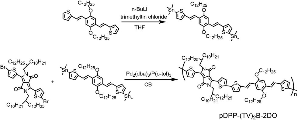 | ||
| Scheme 1 Synthetic scheme of pDPP-(TV)2B-2DO used in this study. | ||
A thermally-grown, 300 nm thick silicon dioxide (SiO2) on a highly n-doped Si substrate was used as a gate dielectric. The SiO2 surface was modified with a reactive dimethylchlorosilane-terminated polystyrene (PS-Si(CH3)2Cl, number average molecular weight, Mn = 8.0 kDa, weight average molecular weight, Mw = 8.6 kDa, Polymer Source Inc.). 6 mg of PS-Si(CH3)2Cl were dissolved in 1 mL of anhydrous toluene, and thin films were spun-cast on UVO3-treated SiO2/Si substrates from the solution in an N2-purged glove box.9 Next, the polymer-coated SiO2 samples were thermally treated at 110 °C for 2 h, and followed by rinsing with an excess volume of toluene to remove the no-grafted polymer residue. Approximately 20–25 nm thick pDPP-(TV)2B-2DO films were spun-cast on the PS-grafted SiO2 dielectrics (referred to as gPS-SiO2) from a 5 mg mL−1 solution prepared with CF. Some were further annealed at a temperature (T) ranging from 150 to 300 °C for 1 h, based on the thermal behavior of the copolymer using differential scanning calorimetry (DSC) (Fig. 1d). Finally, 80 nm-thick Au S/D electrodes were thermally evaporated on the pDPP-(TV)2B-2DO films through a shadow-mask: the channel length (L) and width (W) were 100 and 1500 μm, respectively.
 | ||
| Fig. 1 Typical characteristics of pDPP-(TV)2B-2DO used in this study: (a) UV-vis spectra in a CF solution and spun-cast films. (b) CV curve of a spun-cast film. (c) TGA heating and (d) DSC heating and cooling curves obtained at a constant rate of 10 °C min−1. | ||
Characterization
The molecular weights (Mn and Mw) and polydispersity index (PDI, Mw/Mn) of pDPP-(TV)2B-2DO were determined by gel permeation chromatography (GPC, calibrated with PS standards, Waters, M590) in chlorobenzene (80 °C). The chemical compositions of intermediate materials and pDPP-(TV)2B-2DO were obtained from 1H nuclear magnetic resonance (NMR, Varian, Mercury Plus 300 MHz spectrometer) and 13C NMR analyses, respectively. The thermal stability of the copolymer was measured by thermogravimetric analysis (TGA, TA Instrument, Q50), which was operated under an N2 atmosphere. Additionally, DSC (TA Instrument, Q20) was performed on powder-like polymers with a scan rate of 10 °C min−1. UV-vis absorption spectra of the copolymer in a dilute CF solution and spun-cast films before and after annealing at various values of TAs were measured using a UV-vis spectrometer (JASCO, JP/V-570). Cyclic voltammetry (CV) for the copolymer was performed using an electrochemical analyzer (CH Instruments) in a CF solution containing ferrocene as a supporting electrolyte at a scan rate of 50 mV s−1: a glassy carbon disk (ca. 0.05 cm2) coated with a thin polymer film, an Ag/AgNO3 electrode, and a platinum wire were used as the working, reference, and counter electrodes, respectively.22All the morphologies of the pDPP-(TV)2B-2DO films on the gPS-SiO2 surfaces were observed by atomic force microscopy (AFM, Bruker, Multimode 8). The current–voltage (I–V) measurement of the OFETs was conducted in an N2-purged glove box at room temperature (RT), using a Keithley 4200 SCS. The values of μFET were calculated from the drain current–gate voltage (ID–VG) transfer curves of the OFETs operated under the saturation region (at drain voltage, VD = −30 V) and the following equation: ID = μFETCiW(2L)−1(VG − Vth)2, where Ci is the capacitance per unit area of the dielectric and Vth is the threshold voltage. The Ci value (approximately 10.8 nF cm−2) for the gPS-SiO2 dielectric, sandwiched between Au dots and a highly-doped n-type Si (100) substrate, was measured with an Agilent 4284A Precision LCR meter. Two-dimensional (2D) grazing-incidence X-ray diffraction (GIXD) was performed on all films at beamlines 3C, 6D, and 9A of the Pohang Acceleration Laboratory (PAL), Korea. The incident angle of the X-ray beam on the sample remained below 0.18°.9
Results and discussion
The chemical structures of the intermediate compounds, D unit, A units, and D–A copolymer synthesized were identified by 1H-NMR and 13C-NMR (Fig. S1–S7 in the ESI†). 60 kDa (Fig. S8 in the ESI†) pDPP-(TV)2B-2DO exhibited a solubility of more than 5 mg in 1 mL of common solvents due to the benefit of the long branched alkyl and alkoxy substituents, such as bis(2-decyltetradecyl) and DO moieties, respectively, on the DPP and (TV)2B-2DO blocks (Scheme 1).24 Fig. 1a represents the UV-vis absorption spectra of the copolymer in a CF solution and the corresponding spun-cast films before and after annealing at 150 and 200 °C, respectively. The absorption maximum λmax values are summarized in Table 1. First, the UV-vis spectrum of pDPP-(TV)2B-2DO dissolved in CF showed three absorption peaks at 470, 677, and 734 nm, respectively. Additionally, the absorption peaks obtained from the spun-cast and further annealed thin films were broadened and red-shifted, and an absorption onset at 890 nm also appeared. The red shift of the absorption peaks from the solution to a solid state confirmed that the electron donating and flexible DO moieties did not degrade the conjugated conformation of the copolymer in solution. It was expected that the flexibility effectively contributed to improved π-conjugated and -overlap chain ordering in the condensed solid films during the thermal annealing.25The highest occupied molecular orbital (HOMO) and lowest unoccupied molecular orbital (LUMO) of the copolymer were calculated from the CV profile (Fig. 1b) and the following equation: EHOMO = −(Eoxonset + 4.50) (eV), ELUMO = −(Eredonset + 4.50) (eV), where Eoxonset and Eredonset are the onset oxidation potential and onset reduction potential versus Ag/Ag+, which values are 0.94 and −0.66 V, respectively.26 The HOMO, LUMO levels, and HOMO–LUMO bandgap (Eg) energies were calculated as −5.44, −3.96, and 1.48 eV, respectively (Table 1). The TGA profile of the powder-like copolymer showed approximately 5% weight losses at 429 °C (Fig. 1c). Additionally, the copolymer showed a melting temperature near 241 °C, as determined by DSC analysis (Fig. 1d), but the crystallization peak of the molten copolymer was not clearly observed during the subsequent cooling at 10 °C min−1. This behavior may be attributed to a highly-condensed state, where the molten chains require sufficient long time to form ordered aggregates.
In order to estimate the chain rigidity of the copolymer, density functional theory (DFT) calculations of a simplified dimer of pDPP-(TV)2B-2DO was conducted using B3LYP functional and 6-31G(d) basis sets, and the corresponding result illustrates that the HOMO and LUMO states of the dimer were well delocalized along the conjugated chain (Fig. 2). In the D–A dimer, the divinylbenzene segment tended to increase the backbone planarity and rigidity because the vinyl linker reduced the steric repulsion between aromatic rings. The bulky 2DO moieties improved the solubility and electron density of the pDPP-(TV)2B-2DO copolymer compared to non-substituted systems.27,28 However, the long DO substituents at the 3,5-positions of benzene would protrude out the conjugated plane and hinder the intermolecular π–π stacking, suppressing the device performance, which is discussed in later.
 | ||
| Fig. 2 Schemes of DFT-predicted (a) HOMO and (b) LUMO maps for pDPP-(TV)2B-2DO. | ||
As channel layers in OFETs, 20–25 nm-thick pDPP-(TV)2B-2DO films were spun-cast on gPS-SiO2 dielectrics from CF, and some were further annealed at different TA values of 150, 200, 250, and 300 °C for 1 h, respectively. Fig. 3a–e show typical AFM topographies of these spun-cast copolymer films before and after annealing. First, AFM topography of the as-spun film showed a featureless, smooth layer (Fig. 3a). Via post-annealing at different TA values, the pDPP-(TV)2B-2DO films contained various ordering. Below the Tm (241 °C) of the copolymer, TA-induced aggregates were confined to small-sized nanodots (Fig. 3b and c). In contrast, the 250 and 300 °C-annealed films showed the better-extended nanostructures such as nano-rods and -fibrils. The ordered nanorods in the 250 °C-annealed film were laterally interconnected with apparent grain boundaries (GBs), which slightly increased the surface roughness (Rq) value up to 1.40 nm, in comparison to those (0.65–0.80 nm) of the other films (Fig. 3f). Additionally, the 300 °C-annealed film seemed to have longer fibril-like domains but were locally dewetted due to the much higher TA than Tm, as indicated in optical microscopy images (Fig. S9 in the ESI†). The lateral disconnection of π-overlapped structures degraded the charge-carrier transport in OFETs (which will be discussed later).9
 | ||
| Fig. 3 (a–e) AFM topographies of pDPP-(TV)2B-2DO films spun-cast on gPS-SiO2 surfaces (a) before and (b–e) after annealing at various TA values for 10 min: (b) 150, (c) 200, (d) 250, and (e) 300 °C. (f) Cross-sectional height profiles extracted from the lines in (a)–(e). | ||
Fig. 4a–e represent the typical 2D GIXD patterns of these pDPP-(TV)2B-2DO films before and after annealing at different values of TA. Additionally, 1D X-ray profiles extracted along the in-plane (Qxy) and out-of-plane (Qz) directions from the 2D GIXD patterns (Fig. S10 in the ESI†). The 2D GIXD pattern of the as-spun film exhibited weak X-ray diffractions. Interestingly, the (h00) and (010) reflections were preferentially oriented along the Qxy and Qz axes, respectively, suggesting that the copolymer chains had a preferred orientation with a face-on conformation on the surface: approximately 81% of the chains kept the face-on conformation, as determined from the deconvolution of the azimuthal scan profiles extracted at Q(100) ∼ 0.27 Å−1 (Fig. 4f and S11 in the ESI†). With further annealing, the film crystallinities and the portion of edge-on chains were considerably improved with increasing TA, as determined by the intensities of the out-of-plane X-ray profiles (Fig. S10a†). Note that the chain and crystal orientations in the annealed films drastically changed near Tm of the copolymer. At TA < Tm, i.e., under a cold crystallization condition, two discernible chain conformations competed and the edge-on chains were thermodynamically developed from less-ordered regions during annealing. When the early face-on chains were completely disordered at TA greater than Tm, e.g., 250 and 300 °C, the chain conformation completely disappeared and changed to edge-on in the annealed films (Fig. 4d and e).
 | ||
| Fig. 4 (a–e) 2D GIXD patterns of the pDPP-(TV)2B-2DO films spun-cast (a) before and (b–e) after annealing at different TA values: (b) 150, (c) 200, (d) 250, and (e) 300 °C. (f) Variations in edge-on and face-on chain formations in the copolymer films before and after thermal annealing (the values were calculated from the azimuthal X-ray scan profiles extracted at Q(100) from (a)–(e), Fig. S11 in the ESI†). | ||
Based on the periodic (h00) reflections along the Qz axis and Bragg's law (d = 2π/Q),29 the domain spacing between the (100) planes, d(100), was calculated as 24.17 Å, independent of annealing. Similarly, the intermolecular π–π overlap distance, i.e., between the (010) planes, d(010) increased from 3.81 to 3.88 Å with an increase in TA. It has been reported that typical semiconducting polymers had the following d(010) values: 3.81–3.87 Å (P3HT),10 −3.72 Å (pBTTT-C14),15 and 3.56–3.95 Å (some DPP-based copolymers).9,18,22 Compared with these conjugated polymers, the relatively wider π–π stacking between the pDPP-(TV)2B-2DO chains was expected to degrade the charge-carrier transport along the π–π stacked conducting paths.
To characterize the ordering-dependent electrical properties of the pDPP-(TV)2B-2DO films, OFETs containing the as-spun and annealed films on gPS-SiO2 gate dielectrics were fabricated with top-contact Au S/D electrodes. Fig. 5 shows typical ID–VG transfer curves of pDPP-(TV)2B-2DO OFETs operated in the saturation regime (VD = −30 V). Every kind of OFETs was measured for more than 8 different samples, and the whole results were summarized in Fig. S12 in the ESI.† Additionally, ID–VD output curves of all the samples present typical p-type transistor behaviors (Fig. S13 in the ESI†).24 Electrical properties of the OFETs are summarized in Table 2. After annealing, a slight VG-sweep hysteresis of 1–2 V in the as-spun film became disappeared, with the 250 °C-annealed film exhibiting no sweep hysteresis in the OFET (Fig. 5a and d).
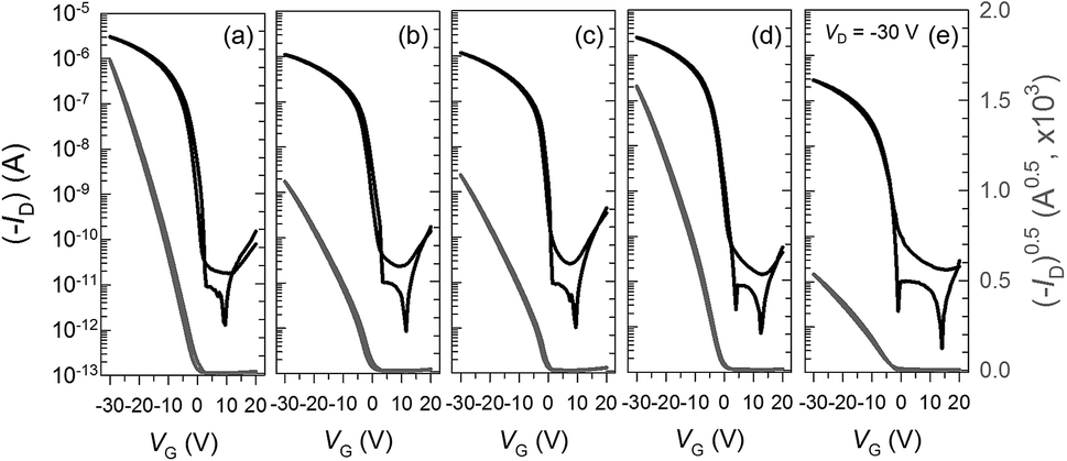 | ||
| Fig. 5 ID–VG transfer curves of pDPP-(TV)2B-2DO based OFETs (a) before and (b–e) after annealing at different TA values: (b) 150, (c) 200, (d) 250, (e) 300 °C. | ||
| OFET | TA (°C) | μFET (cm2 V−1 s−1) | Vth (V) | Ion/Ioff |
|---|---|---|---|---|
| As-spun | — | 0.07 ± 0.003 | −0.5 ± 0.2 | >105 |
| 150 °C-annealed | 150 | 0.04 ± 0.006 | 0.5 ± 0.1 | >105 |
| 200 °C-annealed | 200 | 0.03 ± 0.006 | 0.7 ± 0.2 | >105 |
| 250 °C-annealed | 250 | 0.08 ± 0.004 | −0.2 ± 0.1 | >106 |
| 300 °C-annealed | 300 | 0.01 ± 0.003 | −2.5 ± 0.2 | >105 |
In OFETs, the as-spun film yielded an average μFET value of 0.07 cm2 V−1 s−1, as well as a threshold voltage (Vth) of −0.5 V near zero and an on/off current ratio (Ion/Ioff) greater than 105. Unexpectedly, the 150 and 200 °C-annealed films containing better-ordered domains with degraded μFET values of 0.04 and 0.03 cm2 V−1 s−1 in OFETs, respectively, corresponding to 57 and 43% of μFET of the as-spun film system (μFET,as). Similar to the as-spun OFET, the 250 °C-annealed pDPP-(TV)2B-2DO OFETs yielded μFET values of up to 0.08 cm2 V−1 s−1 (115% of μFET,as), as well as Ion/Ioff values greater than 106 and Vth ∼ 0 V. As expected from the discontinuous film morphology of the 300 °C-annealed film, the corresponding OFET showed a severe decrease of μFET down to levels of 0.01 cm2 V−1 s−1 (14% of μFET,as) due to the dewetting behavior as mentioned above (Fig. S9 in ESI†), as well as a negative Vth shift to −2.5 V.
Excellent μFET values of most organic semiconducting films are primarily related to two-dimensional charge carrier transport along both the edge-on π-conjugated backbones and π-overlapped neighbours on the dielectric surface. In semiconducting films, the ordered structures drastically affected the charge carrier transport.30 Recently, Cho and co-workers synthesized a series of DPP-based copolymers containing intentionally-locked and -unlocked D blocks to induce the preferential chain conformations in the cast films.31 The μFET of the thin films, including vertical π-overlap conducting paths of the face-on chains on gate dielectrics originating from the non-covalent sulfur–oxygen (S–O) interaction between thiophene (T) and dimethoxy-benzene units, decreased by up to 50% in the unlocked copolymer system (ca. 0.2 cm2 V−1 s−1), replacing the derivative of non-substituted benzene. Whereas, the fluorine-substituted chains yielding parallel π-overlap direction showed the highest μFET values up to 6 times greater. The increase in conjugated coherence length of the edge-on chains along the S–D electrodes in OFETs could induce better charge-carrier transport in the semiconducting film. In contrast, Gargi et al. reported that the in-plane π-overlap of the edge-on P3HT chains on gate dielectrics was not necessary to enhance the electrical performance of OFETs, if the chains were highly ordered.32
Fig. 6 represents the conformational changes of the pDPP-(TV)2B-2DO chains in the cast films starting from mostly a face-on, intermediate mixture, to the edge-on form with increasing TA. As mentioned above, the best OFETs were obtained for the pDPP-(TV)2B-2DO films including either face-on or edge-on chains preferentially oriented on the gate dielectrics. In the case of the pDPP-(TV)2B-2DO copolymer synthesized as a semiconducting polymer, the face-on conformation of the backbones was kinetically preferred on the substrate under a fast solvent evaporation, while the ordered edge-on chains competed with the face-on domains in the annealed films and became dominant after annealing at a high TA near its Tm ∼ 241 °C. When the pDPP-(TV)2B-2DO chains were preferentially π-overlapped with either face-on or edge-on conformations on the dielectric surface (Fig. 6a and b), the mobile charge carriers injected into the conducting path near the dielectric interface tended to transfer effectively along the S–D electrodes (laterally positioned), due to the long π-overlapped extension between the conjugated chains. Particularly, the face-on conjugated chains superposed on the gate dielectric were expected to effectively transfer the charge carriers along the π–π overlap direction with occasional hopping behavior, although the as-spun pDPP-(TV)2B-2DO film was less crystalline. In contrast, the existence of the mixed chain conformations in the semiconducting film severely degraded the charge carrier transport because the short π-overlap-driven complex of the conducting paths surrounded by the insulating side-substituents interrupted the charge carrier transport (Fig. 6c). Therefore, it is important to keep consistency in the π-overlap structures of conjugated polymers for high-performance OFETs, i.e., the π-overlap of edge-on semiconducting polymers on gate dielectrics is not necessary to enhance the electrical performance of OFETs if the chains can be highly consistent along a given axis.
 | ||
| Fig. 6 Schematic diagrams of the charge-carrier transport behaviors in pDPP-(TV)2B-2DO films containing different conformations of π-conjugated chains: (a) face-on, (b) edge-on, and (c) mixed chain conformations (yellow-colored arrows represent the transport paths of the charge carriers along the π-overlapped chains). | ||
Conclusions
A new DPP based conjugated copolymer, pDPP-(TV)2B-2DO, that includes DPP as an acceptor and 1,4-bis((E)-2-(thiophen-2-yl)vinyl)benzene as a donor was synthesized by Stille-coupling polymerization. The introduction of the divinylbenzene segment increased the planarity and rigidity of the polymer as the two vinyl linkers reduced the steric repulsion of benzene, while the 1,4-didodecyloxy groups on benzene improved the solubility and flexibility to control the chain conformations. The 60 kDa pDPP-(TV)2B copolymer showed good solubility in organic solvents and was well ordered during the film procedures. The copolymer thin films were spun-cast on polymer-treated SiO2 from chloroform and annealed at a temperature ranging from 150 to 300 °C for 1 h. Featureless aggregates of the face-on copolymer by the bulky 1,4-didodecyloxy benzene in the D block were dominant in the as-spun film and transferred to ordered rods or fibrils after annealing at a TA greater than Tm (=241 °C). As-spun and 250 °C-annealed pDPP-(TV)2B films showed very discernible crystal structures in terms of morphology and orientation, but their based OFETs yielded μFET values of 0.07 and 0.08 cm2 V−1 s−1, respectively, as well as Ion/Ioff values greater than 106 and Vth nearly 0 V. The electrical performance of the OFETs based on the pDPP-(TV)2B-2DO films, which contained physically-controlled chain conformations, strongly supports that it is necessary to keep consistency in π-conjugated ordering of semiconducting polymers for high-performance OFETs.Acknowledgements
This work was supported by grants from the Center for Advanced Soft Electronics under the Global Frontier Research Program (2012M3A6A5055225), General Research Program (2013R1A12063963) of the Ministry of Education, Science, and Technology (MEST), Korea, and NRF by MSIO (20151A2A1A10055620).References
- H. Sirringhaus, P. J. Brown, R. H. Friend, M. M. Nielsen, K. Bechgaard, B. M. W. Langeveld-Voss, A. J. H. Spiering, R. A. J. Janssen, E. W. Meijer, P. Herwig and D. M. de Leeuw, Nature, 1999, 401, 685 CrossRef CAS.
- G. Wang, J. Swensen, D. Moses and A. J. Heeger, J. Appl. Phys., 2003, 93, 6137 CrossRef CAS.
- B. S. Ong, Y. Wu, P. Liu and S. Gardner, J. Am. Chem. Soc., 2004, 126, 3378 CrossRef CAS PubMed.
- H. Kong, D. S. Chung, I. N. Kang, J. H. Park, M. J. Park, I. H. Jung, C. E. Park and H. K. Shim, J. Mater. Chem., 2009, 19, 3490 RSC.
- B. H. Hamadani, D. J. Gundlach, I. McCulloch and M. Heeney, Appl. Phys. Lett., 2007, 91, 243512 CrossRef.
- M. Heeney, C. Bailey, K. Genevicius, M. Shkunov, D. Sparrowe, S. Tierney and I. McCulloch, J. Am. Chem. Soc., 2005, 127, 1078 CrossRef CAS PubMed.
- H. Yan, Z. H. Chen, Y. Zheng, C. Newman, J. R. Quinn, F. Dotz, M. Kastler and A. Facchetti, Nature, 2009, 457, 679 CrossRef CAS PubMed.
- M. Jang, J. Kim, D. Hwang and H. Yang, ACS Appl. Mater. Interfaces, 2015, 7, 12781 CAS.
- M. Jang, S. H. Kim, H. Lee, Y. Kim and H. Yang, Adv. Funct. Mater., 2015, 25, 3833 CrossRef CAS.
- D. Venkateshvaran, M. Nikolka, A. Sadhanala, V. Lemaur, M. Zelazny, M. Kepa, M. Hurhangee, A. J. Kronemeijer, V. Pecunia and I. Nasrallah, et al., Nature, 2014, 515, 384 CrossRef CAS PubMed.
- H. Yang, T. J. Shin, L. Yang, K. Cho, C. Y. Ryu and Z. Bao, Adv. Funct. Mater., 2005, 15, 671 CrossRef CAS.
- P. Sonar, T. R. B. Foong and A. Dodabalapur, Phys. Chem. Chem. Phys., 2014, 16, 4275 RSC.
- Y. Deng, Y. Chen, X. Zhang, H. Tian, C. Bao, D. Yan, Y. Geng and F. Wang, Macromolecules, 2012, 45, 8621 CrossRef CAS.
- M. Jang and H. Yang, J. Nanosci. Nanotechnol., 2012, 12, 1220 CrossRef CAS PubMed.
- I. McCulloch, M. Heeney, C. Bailey, K. Genevicius, I. McDonald, M. Shkunov, D. Sparrowe, S. Tierney, R. Wagner and W. Zhang, et al., Nat. Mater., 2006, 5, 328 CrossRef CAS PubMed.
- P. Sonar, S. P. Singh, E. L. Williams, Y. Li, M. S. Soh and A. Dodabalapur, J. Mater. Chem., 2012, 22, 4425 RSC.
- P. Sonar, J. Zhuo, L. Zhao, K. Lim, J. Chen, A. J. Rondinone, S. P. Singh, L. Chua, P. K. H. Ho and A. Dodabalapur, J. Mater. Chem., 2012, 22, 17284 RSC.
- I. Kang, T. K. An, J. Hong, H. Yun, R. Kim, D. S. Chung, C. E. Park, Y. Kim and S. Kwon, Adv. Mater., 2013, 25, 524 CrossRef CAS PubMed.
- H. Yun, H. H. Choi, S. Kwon, Y. Kim and K. Cho, Chem. Mater., 2014, 26, 3928 CrossRef CAS.
- T. Ha, P. Sonar and A. Dodabalapur, Phys. Chem. Chem. Phys., 2013, 15, 9735 RSC.
- I. Osaka and K. Takimiya, Polymer, 2015, 59, A1 CrossRef CAS.
- J. Kim, J. B. Park, I. H. Jung, A. C. Grimsdale, S. C. Yoon, H. Yang and D. Hwang, Energy Environ. Sci., 2015, 8, 2352 CAS.
- Y. Kim, D. X. Long, J. Lee, G. Kim, T. J. Shin, K. Nam, Y. Noh and C. Yang, Macromolecules, 2015, 48, 5179 CrossRef CAS.
- K. Chen, H. Li, C. Chen, S. Yang, B. R. Hsieh and C. Hsu, Macromolecules, 2005, 38, 8617 CrossRef CAS.
- M. Zheng, L. Ding and F. E. Karasz, Macromol. Chem. Phys., 2002, 203, 1337 CrossRef CAS.
- Y. Lu, Z. Xiao, Y. Yuan, H. Wu, Z. An, Y. Hou, C. Gao and J. Huang, J. Mater. Chem. C, 2013, 1, 630 RSC.
- H. Qin, L. Li, F. Guo, S. Su, J. Peng, Y. Cao and X. Peng, Energy Environ. Sci., 2014, 7, 1397 CAS.
- C. Chang, Y. Cheng, S. Hung, J. Wu, W. Kao, C. Lee and C. Hsu, Adv. Mater., 2012, 24, 549 CrossRef CAS PubMed.
- D. Gidalevitz, Z. Huang and S. A. Rice, Biophys. J., 1999, 76, 2797 CrossRef CAS PubMed.
- I. Botiz and N. Stingelin, Materials, 2014, 7, 2273 CrossRef CAS.
- H. G. Kim, B. Kang, H. Ko, J. Lee, J. Shin and K. Cho, Chem. Mater., 2015, 27, 829 CrossRef CAS.
- D. Gargi, R. J. Kline, D. M. DeLongchamp, D. A. Fischer, M. F. Toney and B. T. O'Connor, J. Phys. Chem. C, 2013, 117, 17421 CAS.
Footnotes |
| † Electronic supplementary information (ESI) available. See DOI: 10.1039/c6ra14677e |
| ‡ M. P. and K. H. P. contributed equally. |
| This journal is © The Royal Society of Chemistry 2016 |