DOI:
10.1039/C6RA14388A
(Paper)
RSC Adv., 2016,
6, 80011-80016
Voltage pulse controlling multilevel data ferroelectric storage memory with a nonepitaxial ultrathin film†
Received
3rd June 2016
, Accepted 1st August 2016
First published on 9th August 2016
Abstract
Multilevel data ferroelectric storage memory is a breakthrough for addressing low density in ferroelectric random access memories. However, the application of the multilevel data ferroelectric storage memory is limited by high cost and difficulty to prepare high quality epitaxial films. Herein, we create a multilevel data ferroelectric storage memory with a non-epitaxial ferroelectric ultrathin film to overcome these issues. Through controlling the polarization switching and oxygen vacancy migration with the voltage pulses, we demonstrated that voltage-controlled barrier heights yield a memristive behavior with resistance variations. Moreover, we achieved eight logic states, which are written and read easily. Our results suggest new opportunities for ferroelectrics as high density non-volatile memories.
1 Introduction
As the development trend of device miniaturization, the technology is struggling with a challenging scalability problem.1 To overcome this issue, increasing the storage density by realizing multilevel data storage memory is an expeditious way. Ferroelectric memories are of high endurance,2 resistant to radiation,3 fast read/write time,4 and low power consumption.5 They attract many scientists' attention because of their multilevel data storage potential.6–10 According to the research of domain walls, people have found that charged domain walls have conductibility; moreover, charged domain walls can stay at different states with different conductibility.6–9 The other way to achieve multilevel data storage is to control the ratio of different domain orientations in every ferroelectric memory unit, causing the change in the barrier height to control the tunnel current.10 This way consumes little energy and is effective to achieve multilevel data storage with the sandwich structure of the storage unit.10 The write and read processes of these devices extremely depend on conductive atomic force microscopy (CAFM) or piezoelectric atomic force microscope (PFM) technology. Moreover, these two types of devices are almost based on ferroelectric epitaxial films.11–14 However, the cost to prepare high quality epitaxial films is very high, and there are still several difficulties in preparing epitaxial thin films. All these limit the application of the multilevel data ferroelectric storage memories. If the polycrystalline ferroelectric thin films could be used to replace the epitaxial thin films, it would be much easier and cheaper to prepare the multilevel data storage memories. Ferroelectricity may decrease because of the different orientation grains in the polycrystalline ferroelectric films, particularly in the ultrathin films. Polycrystalline ferroelectric ultrathin films may be able to play an important role to achieve the multilevel data ferroelectric storage memory by controlling ferroelectricity and oxygen vacancy migration together, which is similar to the way of controlling polarization and oxygen vacancies in an epitaxial ferroelectric tunnel memristor.15 In this study, we show a type of memory that can realize multi-states with polycrystalline ferroelectric ultrathin films by controlling the polarization switching and oxygen vacancy migration. The device that uses voltage pulse control is satisfying in state reproducibility and integrating with the silicon technology in modern microelectronics. The different resistance states (RSs) of the device can be distinguished clearly, particularly written and read easily. Therefore, the application of polycrystalline ferroelectric thin films may be extended to fabricate the multi-level memories. All these show the strong promise for the practical application of multilevel data ferroelectric storage memories.
2 Experimental sections
Sample preparation
Non-epitaxial PbZr0.52Ti0.48O3 (PZT) films with different thicknesses have been grown by laser molecular beam epitaxy (LMBE) on As-doped Si substrates. During the deposition of the PZT layer substrate, the temperature was maintained at 625 °C with the chamber oxygen pressure kept at 22 Pa. A 3 nm SiOx layer was formed in the preparation of the PZT layer because of oxygen diffusion. The samples were cooled to room temperature in an oxygen atmosphere at 22 Pa. Pt dot electrodes were fabricated by d.c. sputtering through a shadow mask of about 100 μm in diameter at room temperature, as shown in Fig. 1.
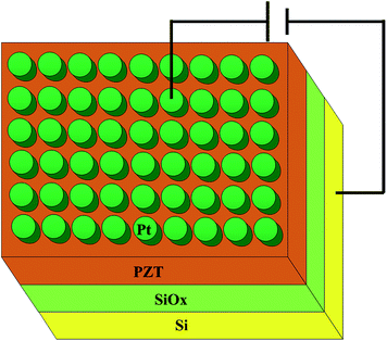 |
| | Fig. 1 Schematic of the device. The diameter of the Pt dot is about 100 μm. As doped Si substrate acts as the bottom electrode. | |
Characterization
Structural characteristics were performed using X-ray diffraction (D/MAX-2500/PC). Electrical properties were measured using a Radiant technologies precision workstation ferroelectric test system. Controlled ferroelectric barrier heights were written using an Agilent B1500A semiconductor device analyzer by applying d.c. voltage pulses, and the I–V measurement characteristic were also measured on it. The piezoresponse Atom Force Microscopy (AFM) images were obtained using the AFM (MUITIMODEPICOFOREE) with a conductive AFM tip. Cross-sectional TEM image of PZT/SiOx/Si heterostructures was obtained using Transmission Electron Microscopy (JEM-2100).
3 Results and discussions
Structural characteristics of PZT/SiOx/Si heterostructures and Si substrate were carried out using X-ray diffraction (XRD); Fig. 2 present the peaks at the (200), (211) and (212) planes of PZT; Fig. 3(a) shows the hysteresis loops of Pt/PZT/SiOx/Si; Fig. 3(b) shows local PFM phase hysteresis loop of a 2 nm thick PZT thin film. It has been proved that the ultrathin ferroelectric films directly grown on Si substrates still retain excellent electrical properties.16 Fig. 4 is the TEM result of the PZT/SiOx/Si heterostructure, demonstrating that the PZT layer is not the epitaxial thin film with a thickness of about 2 nm, demonstrating that the SiOx layer is about 3 nm.
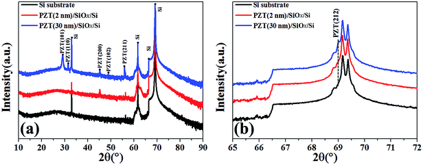 |
| | Fig. 2 (a) XRD patterns of PZT/SiOx/Si heterostructures and Si substrate at various 2θ. (b) (212) peak shift of XRD spectra. The thicknesses of the PZT films are about 2 nm and 30 nm. | |
 |
| | Fig. 3 (a) Hysteresis loops of 2 nm thick PZT layer on As doped silicon wafer with Pt top electrode. Hysteresis loops measured by Radiant technologies precision workstation ferroelectric test system. (b) Local PFM phase hysteresis loop measured by PFM. | |
 |
| | Fig. 4 Cross-sectional TEM image of PZT/SiOx/Si heterostructure. | |
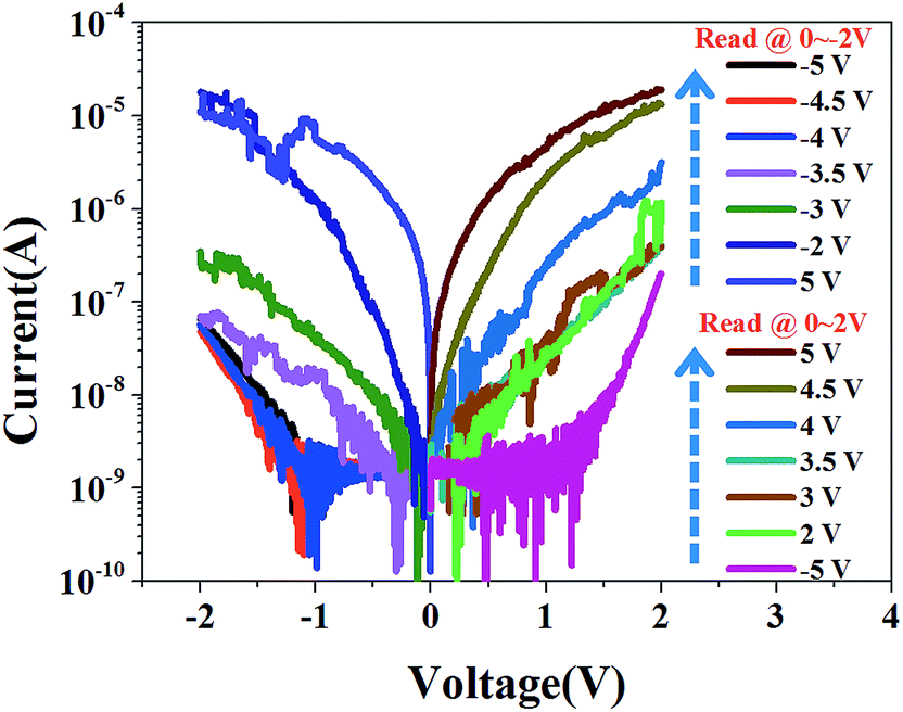
The lowest resistance state (LRS) and highest resistance state (HRS) of the Pt/PZT/SiOx/Si cell were written at 5 V and −5 V, respectively. In order to insure the exactitude of the test, the read voltage was swept from 0 V to positive voltage or negative voltage. As shown in Fig. 5, we can read LRS from 0 V to 3 V (blue line) and clearly see the step changes when the negative voltage sweeping is from 0 V to −3 V (red line). Moreover, we can read HRS from 0 V to −3 V (black line) and clearly see the step changes when the positive voltage sweeping is from 0 V to 3 V (purple line). As shown in the inset figure in Fig. 5, the voltage was swept in a sequence of 0 V → 5 V → 0 V → −5 V → 0 V (in logs). The ratio of HRS and LRS is about 3 to 4 orders, which is much higher when compared with the results of the devices with many epitaxial films previously reported.6,10,14 From the inset figure in Fig. 5, we can clearly see the step changes when the negative (positive) voltage sweeping is applied. These steps show the potential of multilevel data storage on a Pt/PZT/SiOx/Si device, and the device may get different RSs by different write processes. However, these step changes do not show all the RSs clearly. In order to investigate all the RSs that the device can achieve, we tested the sample by the processes shown in Fig. 6(a) and (b). In Fig. 6(a) and (b), it shows that a SET (RESET) voltage pulse is required before every write voltage pulse (i.e., before a write voltage pulse of 4 V is applied, a −5 V SET voltage pulse should be applied first). A SET (RESET) voltage pulse is applied to erase the former resistance state of the Pt/PZT/SiOx/Si device, and then voltage pulses with the opposite direction to the SET (RESET) voltage pulse are applied to obtain different RSs.
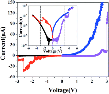 |
| | Fig. 5 Current at various applied voltage. In the inset figure, the voltages are swept from 0 V to −5 V (5 V). The purple line shows that the current is a function of the voltage swept from 0 V to 5 V; the device changes to LRS. The blue line shows the reading of current, which is as a function of the voltage swept from 0 V to 5 V. The red line shows the current as a function of the voltage swept from 0 V to −5 V; the device changes to HRS. The black line shows the reading of current, which is a function of the voltage swept from 0 V to −5 V; the device stays at HRS. | |
 |
| | Fig. 6 (a) and (b) The test process. Red lines and purple lines represent the SET/RESET processes and WRITE processes. Black lines represent the delay. Green lines represent the READ processes. | |
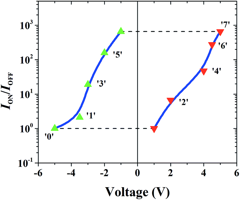
In the processes in Fig. 6(a), the SET voltage is 5 V, and the read process is a voltage pulse or a voltage sweeping. When the resistance of the device is at its lowest, a negative voltage pulse above −1.5 V can switch the resistance state to a higher resistance state. It can be seen that higher negative writing voltage pulses can result in lower current values (or equivalently, the higher resistance states). After the test with the write voltage pulses of −2 V, −3 V, −3.5 V, −4 V, −4.5 V and −5 V, five RSs were achieved. In the processes in Fig. 6(b), the RESET voltage is −5 V. Similar to the former processes, positive voltage pulses can switch the HRS to lower resistance states. After written by voltage pulses of 2 V, 3 V, 3.5 V, 4 V, 4.5 V and 5 V, five RSs were achieved. However, two RSs were the same as two of the former five RSs (LRS and HRS in the two processes are the same). 8 RSs were achieved finally, and the 8 RSs are read by voltage sweepings of 0 V → −2 V or 0 V → 2 V, as shown in Fig. 7. Obviously, more than 8 voltage values can be used to write the RSs. However, considering the application of the device, the different RSs should be distinguished clearly in the read processes. If the ratio of HRS and LRS is much higher, we may obtain more RSs that can be distinguished clearly in the read processes. Fig. 8 shows that the ROFF/RON is as a function of the writing voltage pulse amplitude for the 2 nm thick PZT junction (the RSs are all read with 1 V voltage pulses). The ROFF (resistance of ‘0’ state) value is constant, and only the RON value varies with the writing voltage.
 |
| | Fig. 7 Reading of the RSs. The sequence of write process is from 5 V to −5 V (left) and from −5 V to 5 V (right). −2 V, −3 V, −3.5 V, −4 V, −4.5 V and −5 V are all applied after 5 V voltage pulses applied on the device first. 2 V, 3 V, 3.5 V, 4 V, 4.5 V and 5 V are all applied after −5 V voltage pulses applied on the device first. The left is read from 0 V to −2 V, and the right is read from 0 V to 2 V. The left and right are asymmetric except the LRS and HRS. | |
 |
| | Fig. 8 ROFF/RON as a function of the writing pulse amplitude for the 2 nm thick PZT junction. The ROFF value is constant, and only the RON value varies with the writing voltage. All the RSs are read at 1 V. | |
The tunable and non-volatile nature of electrical resistance of the Pt/PZT/SiOx/Si heterostructure allows us to treat it as a memristor. Although the device has a similar structure to ferroelectric tunnel junctions (FTJs), it is different with common FTJs because of the SiOx layer. When a high voltage of 5 V is applied, it would elevate the field close to ∼0.8 V nm−1; therefore, the switchable polarization of PZT may not be the only reason causing the multi-level storage. Furthermore, the resistive switching of the device is from an insulating state to an almost metallic state, and then back to the insulating state in the effect of the voltage. Therefore, some different things may happen in the resistive switching behavior of the PZT and SiOx layers. The SiOx layer is formed in the preparation of the PZT layer; therefore, many oxygen vacancies are formed in the SiOx layer because of oxygen diffusion during the deposition. Like the resistive switching behaviors in SrTiO3 and TiO2, the oxygen vacancies may be important in our device.17–19 A possible mechanism is shown in Fig. 9. When a high voltage pulse of −5 V is applied on the device, the polarization of PZT film points to SiOx, and most oxygen vacancies are in the SiOx layer; therefore, the device is at ‘0’ state. Then, a positive 2 V is applied to the device, the polarization of PZT film points Pt, and some oxygen vacancies move to the interfaces of PZT and SiOx layers, causing a decrease in the barrier height and large leakage current. When a much higher positive voltage is applied on the device, the polarization value is much larger (as shown in Fig. 3(a)). However, the oxygen vacancies may move into the PZT film, causing a decrease in the PZT barrier height. In the effect of a 5 V voltage pulse, the polarization value may be the highest, but the oxygen vacancies may lead the PZT film to be at an almost metallic state. When a negative 2 V pulse is applied to the device, the oxygen vacancies may move back a little and the polarization will point to SiOx. When the applied negative voltage is increased, the barrier height is also increased. When a −5 V pulse is applied on the device, it will revert back to the ‘0’ state. Obviously, the reverse voltage of PZT polarization is above 1 V in our case (as shown in Fig. 3); therefore, the RSs are stable at 1 V. In order to prove the oxygen vacancy migration in the device, we show a Pt/SrTiO3/SiOx/Si device with a thin non-ferroelectric SrTiO3 film (which is prepared in the same condition with PZT film) in the ESI.† The device can achieve two RSs because of oxygen vacancy migration. A PFM image for each stage in Fig. 9 is also shown in the ESI,† in order to verify the polarization direction and confirm the validity of the proposed mechanism.
 |
| | Fig. 9 A possible mechanism of the multi-level storage. Schematic of the energy barrier diagrams for the OFF and ON states as a function on the external electric field E. | |
An important factor is that the write processes of many multilevel data ferroelectric storage memories previously reported are sensitive to write time at constant voltage values.6–9 Devices with epitaxial films are written using CAFM or PFM through controlling the write time at a certain voltage to control the ratio of different domains orientations. However, less sensitivity in the write time may mean a much higher reliability in the application of the device with respect to the numerous read processes. In our test, when the read voltage sweeping was swept from 0 V to 2 V (−2 V), though we took 103 values by every 2 mV, the RSs were almost unchanged. Furthermore, we only changed the write voltage values in the write processes regardless of the write time. Therefore, the device in our work is much more sensitive to the write voltage value than the write time. In the multilevel data ferroelectric storage memories of domain walls system, the conductivity is mainly caused by the domain walls. Domain wall conductance is a dynamic process that is intrinsically linked to slow polarization dynamics or slow ionic processes such as carrier vacancy segregation processes.6–9 Domain wall acts as an adjustable resistance in the multilevel data ferroelectric storage memory of domain system, while the barrier height mainly acts as the adjustable resistance in our device. Although the two systems have the phenomenon of the multilevel storage, the electrical conduction mechanisms are unalike. Tunnel current is the main role in the 2 nm PZT system with little effect in the domain walls system.
Retention is an important issue for the non-volatile memory cells. We wrote the 8 states as shown in Fig. 6(a) and (b), and read all the states at 1 V to test the retention and to test if the 8 states can be distinguished clearly in the read processes. In 100 s, the RSs are very stable, as shown in Fig. 10(a). 0 (HRS), 1, 3 and 5 states were written at −5 V, −3.5 V, −3 V and −2 V (each write voltage was applied after a 5 V SET process) and 2, 4, 6 and 7 (LRS) states were written at 2 V, 4 V, 4.5 V and 5 V (each write voltage was applied after a −5 V RESET process). Each RS is repetitively written about 30 times, as shown in Fig. 10(b). Most of the RSs can be distinguished clearly at the read voltage of 1 V.
 |
| | Fig. 10 (a) The retention of the Pt/PZT/SiOx/Si memristor. Current as a function of time. (b) Switching between the eight resistance states. Each resistance state is repetitively written about 30 times in cycle. 0 (HRS), 1, 3 and 5 states are written at −5 V, −3.5 V, −3 V, −2 V (each write voltage was applied after a 5 V SET process), and 2, 4, 6 and 7 (LRS) states are written at 2 V, 4 V, 4.5 V, 5 V (each write voltage was applied after a −5 V RESET process). | |
4 Conclusions
In summary, we successfully fabricated a Pt/PZT/SiOx/Si device with a non-epitaxial PZT ultrathin film and demonstrated eight states within it. The ratio of HRS/LRS is really high at about 103 to 104, and the write and read processes are much easier than those in the former reports.6–10,19 The multilevel data ferroelectric storage memory is integrated with silicon technology for electronic devices, which shows a strong promise for future high storage density non-volatile ferroelectric memory applications.
Acknowledgements
This work was supported by the National Natural Science Foundation of China (No. 51572233, 61574121, 11372266 and 11272274), the Hunan Provincial Natural Science Foundation of China (No. 12JJ1007), the Specialized Research Fund for the Doctoral Program of Higher Education (No. 20114301110004) and the Foundation for the Author of National Excellent Doctoral Dissertation of PR China (201143).
References
- G. I. Meijer, Science, 2008, 319, 1625 CrossRef CAS PubMed.
- B. H. Park, B. S. Kang, S. D. Bu, T. W. Noh, J. Lee and W. Jo, Nature, 1999, 401, 682 CrossRef CAS.
- M. Sotome, N. Kida, S. Horiuchi and H. Okamoto, Appl. Phys. Lett., 2014, 105, 041101 Search PubMed.
- D. S. Rana, I. Kawayama, K. Mavani, K. Takahashi, H. Murakami and M. Tonouchi, Adv. Mater., 2009, 21, 2881 CrossRef CAS.
- J. F. Scott, Science, 2007, 315, 954 CrossRef CAS PubMed.
- J. Seidel, L. W. Martin, Q. He, Q. Zhan, Y. H. Chu, A. Rother, M. E. Hawkridge, P. Maksymovych, P. Yu, M. Gajek, N. Balke, S. V. Kalinin, S. Gemming, F. Wang, G. Catalan, J. F. Scott, N. A. Spaldin, J. Orenstein and R. Rames, Nat. Mater., 2009, 8, 229 CrossRef CAS PubMed.
- D. Lee, S. M. Yang, T. H. Kim, B. C. Jeon, Y. S. Kim, J. G. Yoon, H. N. Lee, S. H. Baek, C. B. Eom and T. W. Noh, Adv. Mater., 2012, 24, 402 CrossRef CAS PubMed.
- E. A. Eliseev, A. N. Morozovska, G. S. Svechnikov, V. Gopalan and V. Y. Shur, Phys. Rev. B: Condens. Matter Mater. Phys., 2011, 83, 235313 CrossRef.
- R. K. Vasudevan, A. N. Morozovska, E. A. Eliseev, J. Britson, J.-C. Yang, Y.-H. Chu, P. Maksymovych, L. Q. Chen, V. Nagarajan and S. V. Kalinin, Nano Lett., 2012, 12, 209 CrossRef PubMed.
- A. Chanthbouala, V. Garcia, R. O. Cherifi, K. Bouzehouane, S. Fusil, X. Moya, S. Xavier, H. Yamada, C. Deranlot, N. D. Mathur, M. Bibes, A. Barthélémy and J. Grollier, Nat. Mater., 2012, 11, 860 CrossRef CAS PubMed.
- V. Nagarajan, S. Prasertchoung, T. Zhao, H. Zheng, J. Ouyang, R. Ramesh, W. Tian, X. Q. Pan, D. M. Kim, C. B. Eom, H. Kohlstedt and R. Waser, Appl. Phys. Lett., 2004, 84, 25 CrossRef.
- C.-L. Jia, V. Nagarajan, J.-Q. He, L. Houben, T. Zhao, R. Ramesh, K. Urban and R. Waser, Nat. Mater., 2007, 6, 64–69 CrossRef CAS PubMed.
- Y. Liu, I. C. Infante, X.-J. Lou, L. Bellaiche, J. F. Scott and B. Dkhil, Adv. Mater., 2014, 26, 6132 CrossRef CAS PubMed.
- Z.-P. Li, X. Guo, H.-B. Lu, Z.-L. Zhang, D.-S. Song, S.-B. Cheng, M. Bosman, J. Zhu, Z. L. Dong and W.-G. Zhu, Adv. Mater., 2014, 26, 7185 CrossRef CAS PubMed.
- D. J. Kim, H. Lu, S. Ryu, C.-W. Bark, C.-B. Eom, E. Y. Tsymbal and A. Gruverman, Nano Lett., 2012, 12, 5697 CrossRef CAS PubMed.
- S. Yuan, J. Wang, X. Zhong, J. Huang and Y. Zhou, RSC Adv., 2013, 3, 24362 RSC.
- X. B. Yan, Y. D. Xia, H. N. Xu, X. H. Gao, T. Li, R. Li, J. Yin and Z. G. Liu, Appl. Phys. Lett., 2012, 97, 11 Search PubMed.
- M. H. Lee, K. M. Kim, G. H. Kim, J. Y. Seok, S. J. Song, J. H. Yoon and C. S. Hwang, Appl. Phys. Lett., 2010, 96, 152909 CrossRef.
- P. Hou, J. Wang, X. Zhong and Y. Wu, RSC Adv., 2016, 6, 54113–54118 RSC.
Footnote |
| † Electronic supplementary information (ESI) available. See DOI: 10.1039/c6ra14388a |
|
| This journal is © The Royal Society of Chemistry 2016 |
Click here to see how this site uses Cookies. View our privacy policy here. 
 *abc,
Xiangli Zhong*abc,
Yuan Zhangabc,
Xiong Zhangabc,
Congbing Tanabc and
Bo Liabc
*abc,
Xiangli Zhong*abc,
Yuan Zhangabc,
Xiong Zhangabc,
Congbing Tanabc and
Bo Liabc