
High luminance of CuInS2-based yellow quantum dot light emitting diodes fabricated by all-solution processing†
Jingling Liab,
Hu Jinab,
Kelai Wangac,
Dehui Xieacd,
Dehua Xuabd,
Xueqing Xu*ab and
Gang Xuab
aKey Laboratory of Renewable Energy, Guangzhou Institute of Energy Conversion, Chinese Academy of Sciences, Guangzhou 510640, China. E-mail: xuxq@ms.giec.ac.cn
bUniversity of Chinese Academy of Sciences, Beijing 100049, China
cGuangdong University of Technology, School of Chemical Engineering and Light Industry, Guangzhou 510006, China
dNano Science and Technology Institute, University of Science and Technology of China, Suzhou 215123, China
First published on 14th July 2016
Abstract
In this work, all-solution processed, multi-layer yellow quantum dot light emitting diodes (QLEDs), consisting of a hole transport layer of poly(9-vinylcarbazole), emissive layer of CuInS2/ZnS (ZCIS) QDs, and electron transport layer of ZnO nanoparticles, are fabricated. To improve the carrier-balance in QLEDs, a ligand-exchange strategy is employed to replace n-dodecanethiol that caps the surface of CuInS2/ZnS quantum dots with 2-ethylhexanethiol. After this processing, improvement of current efficiency and external quantum efficiency of QLEDs is achieved. The optimized diodes exhibit a maximum luminance of 2354 cd m−2 and an external quantum efficiency of 0.63%, together with a lower turn-on voltage (decreases from 3.1 V to 2.7 V) using these ligand-exchanged QDs as emitting materials. Furthermore, CuInS2-based QLEDs in our study exhibit color retainability with increasing voltage and prolonged use, and show great promise for practical application.
1. Introduction
The interest in colloidal semiconductor quantum dot-based light emitting diodes (QLEDs) has been growing over the past two decades due to their unique and attractive optoelectronic properties, such as high quantum yield, high color purity and emission tunability,1–4 and are therefore promising for applications in thin film displays and solid-state lighting.5–11 Ever since the first QLEDs were demonstrated in 1994,12 the device performances have rapidly improved in terms of the luminance (L0 > 200![[thin space (1/6-em)]](https://www.rsc.org/images/entities/char_2009.gif) 000 cd m−2), external quantum efficiency (EQE > 20%), current efficiency (ηA > 50 cd A−1) and device stability, as a result of multilateral efforts on synthesizing higher quality QDs, improving the carrier injection/transportation, and designing proper device architectures.13–17 However, the toxicity of high performance of QLEDs remains an unavoidable issue due to the use of cadmium (Cd) which profoundly affects human health. Low toxicity, high photoluminescence quantum yield (QY) materials are of great significance for the development and popularization of QLEDs.
000 cd m−2), external quantum efficiency (EQE > 20%), current efficiency (ηA > 50 cd A−1) and device stability, as a result of multilateral efforts on synthesizing higher quality QDs, improving the carrier injection/transportation, and designing proper device architectures.13–17 However, the toxicity of high performance of QLEDs remains an unavoidable issue due to the use of cadmium (Cd) which profoundly affects human health. Low toxicity, high photoluminescence quantum yield (QY) materials are of great significance for the development and popularization of QLEDs.
Group I–III–VI nanocrystals (NCs) are a potential solution as Cd-free QD emitters. Archetypal compositions of I–III–VI NCs include Cu–In–S, Ag–In–S, Cu–In–Se, Cu–In–Ga–S etc.18–23 Due to their large absorption coefficient plus an intrinsic defect state-related broad band emission, they have been widely utilized as color-converting materials for the fabrication of white lighting devices.11,24–30 Nevertheless, with the growing demand of Cd-free emitters in QLEDs, I–III–VI group QDs, especially CuInS2 (CIS) NCs, have received increasing interest in electroluminescent application.31 In recent years, inspiring results in CIS-based QLEDs have been continually reported. In 2011, Tan et al.32 successfully fabricated red, yellow and green QLEDs with corresponding maximum luminances of 1200 cd m−2, 1160 cd m−2 and 1600 cd m−2 using CIS NCs as the electroluminescent materials. Soon afterwards, Kim and his co-workers33 made a significant improvement on device performance by adopting ZnO nanoparticles (NPs) as the electron transport layer (ETL), in which the devices exhibited a current efficiency of 5.75 cd A−1 and maximum luminance of 2785 cd m−2. With the development of surface modification for QDs, device performance has been further improved. For instance, Gugula et al.22 developed high stability (withstanding 200 h high power blue LED irradiation) CIS-based QLEDs based on a ligand exchange strategy. Accordingly, Bai et al.34 employed this surface modification to improve the electroluminescence of QLEDs. They demonstrated a record external EQE of 3.22% in CIS-based QLEDs. With a ligand exchange occurring on the ZCIS QDs emitter, the maximum luminance and current efficiency of QLEDs increased to 8735 cd m−2 and 9.43 cd A−1, respectively.
Despite the rapid progress, there are still many challenges for CIS-based QLEDs, such as low color purity, high turn-on voltage and more importantly, low efficiency, which is mainly due to the inefficient carrier injection from charge transport layers to the QD emitting layer. Therefore surface modification for QDs that are used in diodes needs to be investigated urgently for the sake of higher conversion efficiency. Moreover, the fabrication of CIS-based QLEDs is usually complicated and could be costly due to the use of a thermal deposition method and expensive transport-layer materials. High luminance, particularly for all-solution processable and low-cost CIS-based QLEDs, needs to be further developed.
Herein, a facile preparation of CIS-based QLEDs is reported. We employ poly(9-vinylcarbazole) (PVK) as the hole transport layer (HTL) and ZnO NPs as the ETL to fabricate cost-effective, solution processable and high luminescent QLEDs. Besides, we demonstrate a feasible ligand exchange using 2-ethylhexanethiol (EHT) to improve the charge balance in QLEDs for the first time. The optimized diodes exhibit a maximum luminance of 2354 cd m−2 and an external quantum efficiency of 0.63%, together with a lower turn-on voltage (∼2.7 V) using these ligand-exchanged QDs as the emitting layer. Furthermore, CIS-based QLEDs in our study exhibit color retainability with increasing voltage and prolonged use, which shows great promise for practical application.
2. Experimental
Synthesis of CuInS2/ZnS (ZCIS) QDs
This synthesis process for ZCIS QDs is based on our previous reports.35 To synthesize ZCIS QDs, the precursor molar Cu/In ratio of 1/4 was used to obtain Cu-deficient QDs. Copper iodide (24 mg, 0.125 mmol) and indium acetate (146 mg, 0.5 mmol) were mixed with DDT (5 mL) in a 50 mL three-necked flask. The reaction mixture was repeatedly degassed under vacuum and purged with nitrogen twice within 15 minutes, during which the mixture was kept stirring. Then the mixture was heated to 100 °C until a clear aqua solution was formed. Subsequently, the temperature was raised to 210 °C with an increasing rate of 5 °C min−1. After 10 minutes of heat preservation, the mixture was rapidly cooled to room temperature. For the process of coating ZnS on CIS NCs, 2.528 g (4 mmol) zinc stearate together with 5 mL ODE was mixed into the obtained CIS NC solutions. Under a N2 atmosphere, the mixture was heated to 240 °C and then maintained at this temperature for 240 minutes. The colloidal NCs were precipitated by the addition of excess acetone, and centrifuged at 8000 rpm for 5 min. Finally, the supernatant was decanted, and the precipitate was redispersed in n-hexane for further analysis.Ligand exchange
In the CIS QD synthesis, DDT serves as the solvent, sulfur source and surface ligand. Therefore, to implement ligand exchange, DDT capped ZCIS (ZCIS-DDT) alloyed QDs were first synthesized. Scheme 1 shows the illustration of the synthetic route and ligand exchange process for EHT capped QDs. EHT capped ZCIS (ZCIS-EHT) QDs through ligand exchange were accomplished by adapting a modified procedure of a previous report.36 In brief, after ZCIS QDs were adequately washed and redispersed in n-octane, 120 μL of 2-ethylhexanethiol was added to a 6 mL colloidal solution that has a concentration of 30 mg mL−1. This mixture was stirred under a nitrogen atmosphere at 60 °C for 12 hours, after which the treated NCs were precipitated by adding excess acetone and redispersed in n-octane for spin-coating a QD layer. | ||
| Scheme 1 Synthetic route of ZCIS QDs and ligand exchange procedure. Here, different surface structures of ZCIS QDs before and after ligand exchange are respectively prepared. | ||
Synthesis of ZnO nanoparticles
ZnO NPs were synthesized based on the protocol reported in the literature.37 3 mmol of Zn acetate hydrate was dissolved in 30 mL of dimethyl sulfoxide (DMSO). 5.5 mmol of tetramethyl ammonium hydroxide (TMAH) dissolved in 10 mL of ethanol was slowly added within 1 minute into the above cationic solution. Then the reaction proceeded at room temperature for 1 hour. Finally, ZnO NPs were precipitated by adding excess of acetone and redispersed into ethanol for the spin deposition of the ETL.Device fabrication
The yellow QLED consists of a multilayered structure of indium tin oxide (ITO), indium tin oxide (ITO, ∼200 nm), poly(ethylenedioxythiophene):polystyrene sulphonate (PEDOT:PSS, ∼35 nm), poly(9-vinylcarbazole) (PVK, ∼45 nm), CuInS2/ZnS core–shell QDs (∼30 nm), ZnO NPs (∼30 nm) and silver (Ag, 120 nm). A patterned ITO glass substrate was sequentially cleaned with methanol, acetone, ethanol, and finally deionized water. First, a hole injection layer (HIL) of PEDOT:PSS (AI 4083, Heraeus) was spin-coated at 4000 rpm for 60 s, and then baked at 150 °C for 30 min. A PVK solution prepared by dissolving 5 mg PVK (average MW = 120000, Aldrich) into 1 mL of chlorobenzene was deposited on top of the HIL as the HTL at 3000 rpm for 60 s and then followed by a 150 °C baking for 30 min. The emitting layer (EML) was spin-deposited using ZCIS QDs dispersed in n-octane with a concentration of ∼25 mg mL−1 at 3000 rpm for 60 s and heating at 70 °C followed. A transparent ethanol solution of ZnO NPs with a concentration of 25 mg mL−1 was then spin-coated at 3000 rpm for 60 s, followed by heating at 70 °C for 30 min. Finally, a 120 nm-thick Ag cathode was deposited on top of the ZnO ETL using a DC magnetron sputtering system, accomplishing the whole structure of QLED. All layers except the Ag cathode were deposited under ambient conditions.
Characterization
Photoluminescence spectra were recorded using a Lambda LS55, and optical absorption spectra were recorded using a Perkin-Elmer Lambda 750 spectrophotometer. Photoluminescence QYs were estimated versus a rhodamine 6G solution in ethanol at an excitation wavelength of 450 nm. The absorbance of all solutions was maintained below 0.1 au at this wavelength to avoid internal filter effects. Fourier-transformed infrared (FTIR) spectra collected using a TENSOR27 Spectrometer and 1H NMR spectra measured using a VANCE III400 were used to distinguish the type of surface ligand on ZCIS QDs. High-resolution transmission electron microscopy (HRTEM) images were obtained using a JEM-2100F TEM at an accelerating voltage of 200 kV. The size distribution of NCs was estimated with the software Image-pro-plus. Samples were prepared by dipping an n-hexane solution of colloidal NCs into a 200 mesh ultrathin carbon grid. Field-emission SEM (Hitachi S-4800) operated at 10 kV was used to obtain information on the thickness of individual layers in multilayered QLEDs and atomic force microscopy (AFM, Bruker Multimode 8) was used to study the surface morphologies of each layer. Electroluminescent (EL) spectra and luminance, current density–voltage characteristics of yellow QLEDs were recorded using an Ocean USB 2000+ spectroradiometer coupled with a Keithley 2420 source under ambient conditions.3. Results and discussion
Materials characterization
The selection of EHT in ligand exchange is based on two considerations. The first one is the potential improvement on device performance. As mentioned in the literature,34 short carbon chain molecular ligands are favorable for carrier transportation. Secondly, we were inclined to obtain oil-soluble QDs for the sake of PVK film quality because the PVK layer is easily damaged by the aqueous QDs solution. Therefore we selected a similar thiol to DDT as the candidate in ligand exchange.In order to classify the type of surface ligand on ZCIS QDs, FTIR measurements were firstly performed. Note that vibrations of C–S and C–H bonds provide the most effective information in differentiating the surface ligands. Fig. S1† shows the FTIR spectra of pure DDT and EHT. It can be seen that the characteristic peak of C–S bonds (νC–S) in DDT appears at 654 cm−1, while that for EHT is located at 669 cm−1. Besides, vibration of C–H bonds (νC–H) varies in different organic molecules, whereas both the symmetrical and asymmetrical stretching vibrations of these bonds in DDT (2854 cm−1 and 2922 cm−1, respectively) appear slightly red-shifted as compared with the corresponding ones in EHT (2859 cm−1 and 2928 cm−1, respectively). Changes of bond strength with different molecular structures may account for these variations. Accordingly, we compare the FTIR spectra (shown in Fig. 1a) of ZCIS QDs before and after ligand exchange. Even DDT- and EHT-capped QDs respectively possess the same νC–H as their corresponding ligand molecules, the flexural vibrations for C–H bonds in DDT- and EHT-capped QDs are completely different (DDT-, 806 cm−1 and 1020 cm−1; EHT-, 914 cm−1). Moreover, νC–S of ZCIS-DDT and ZCIS-EHT QDs emerges at 673 cm−1 and 679 cm−1, respectively, which is also different with those ones in DDT and EHT. This change of νC–S results from the increased C–S bond strength after the S atoms bond with the metal elements of the outer-shell layer. So the different vibration modes imply that various types of ligands have capped the surface of CIS QDs.
 | ||
| Fig. 1 (a) FTIR spectra and (b) 1H NMR spectra of DDT- and EHT-ZCIS QDs. | ||
Further investigation of the type of surface ligand is based on 1H NMR measurements. Fig. 1b displays the 1H NMR spectra of ZCIS-DDT and ZCIS-EHT QDs. It can be observed that the two kinds of QDs possess a very similar spectral pattern. However, the side carbon-chain in EHT has caused some variations in 1H NMR spectra compared with that of DDT, which is helpful to distinguish the type of ligands. As shown in Fig. 1b, the 1H NMR spectrum of EHT-QDs exhibits obvious and differentiated peaks at 1.25 and 1.27 ppm, where the peaks indicate the existence of a CH2 group near the junction of the side chain (signal 4 labeled in Fig. 1b). Further, the peaks at 1.41 ppm (signal 5 marked in Fig. 1b) provide strong evidence for the existence of a CH group in the EHT molecule. All indications mentioned above signify the successful processing of ligand-exchange.
Although DDT surface ligands have been replaced by EHT, the structural and optical properties of ZCIS QDs are maintained after this processing. The TEM images in Fig. 2a and b show that both the ZCIS-DDT and ZCIS-EHT QDs are monodispersed and uniform in shape. Besides, the statistical results reveal that average particle diameter for ZCIS-DDT and ZCIS-EHT QDs, shown respectively in Fig. 2c and d, are nearly the same (3.0 ± 0.8 nm). In line with the results from the TEM observation, the XRD data presented in Fig. 2e indicate that both the ZCIS-DDT and ZCIS-EHT QDs possess the same diffraction pattern, including the diffraction angles and the corresponding full width at half maximum (FWHM). These results also confirm that the size and lattice structure of QDs are maintained after ligand exchange. Fig. 2f shows UV-vis absorption spectra and PL spectra of ZCIS-DDT and ZCIS-EHT QDs. The main fluorescence properties of ZCIS-EHT QDs, such as emission wavelength, FWHM and photoluminescent quantum yield (QY), are very similar to that taken from the sample before ligand exchange. Note that the photoluminescence QYs of ZCIS QDs are 65.1% and 64.5% for the samples before and after ligand exchange, respectively, indicating this ligand-exchange process brought about few effects on the optical properties.
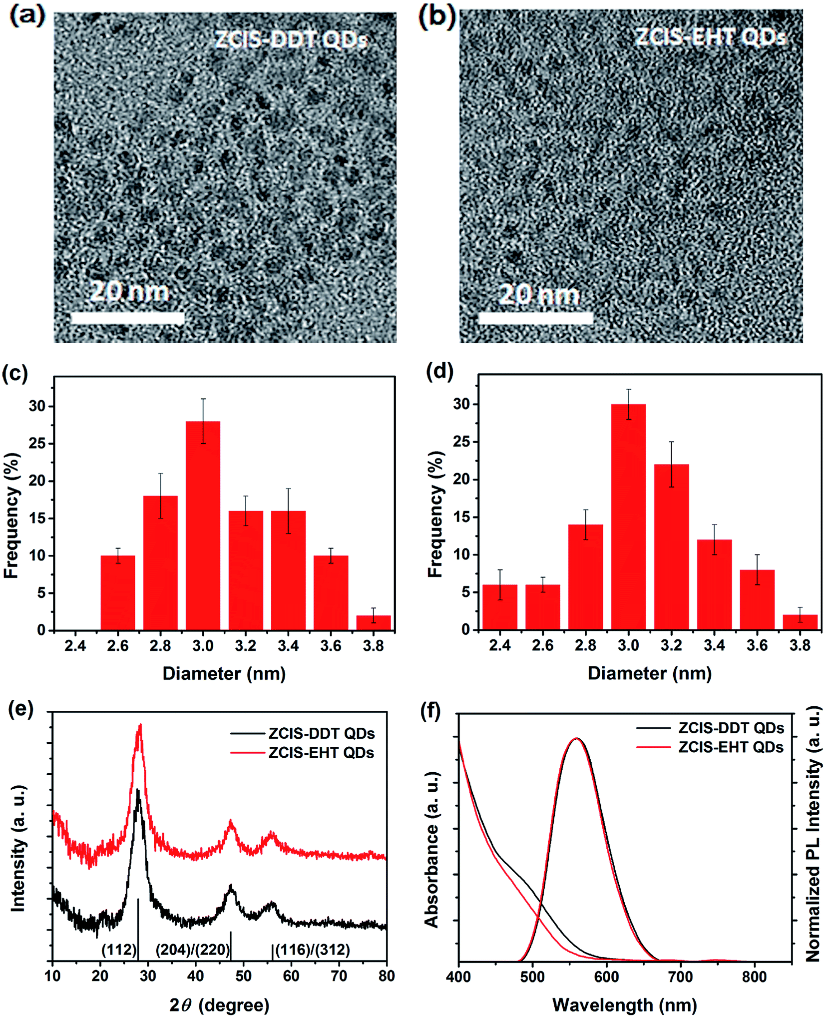 | ||
| Fig. 2 TEM image of (a) ZCIS-DDT and (b) ZCIS-EHT QDs. Histogram of size distribution for (c) ZCIS-DDT QDs and (d) ZCIS-EHT QDs that corresponds to (a) and (b), respectively. (e) XRD patterns, (f) UV-vis absorption and photoluminescence spectra of ZCIS-DDT and ZCIS-EHT QDs. | ||
The employed ZnO NPs are also characterized by TEM, XRD, PL and UV-vis measurements. A TEM image of the ZnO NPs is shown in Fig. S2a,† indicating that the ZnO NPs have a homogeneous size. Lattice fringes can be clearly observed in the high-resolution TEM image shown in the inset, which suggests good crystallinity of the ZnO NPs. The corresponding histogram based on a survey of 100 particles from different regions of the grid is shown in Fig. S2b,† displaying an average size of 4.8 nm for ZnO NPs. Results of the XRD for ZnO NPs are shown in Fig. S2c.† The diffraction pattern suggests that ZnO NPs are crystalline and possess a wurtzite structure similar to that of bulk ZnO, which is consistent with the result referred to in the literature.16 A significant broadening of the characteristic diffraction peaks can be ascribed to the small particle size. A typical absorption spectrum of ZnO NPs is presented in Fig. S2d,† where a distinct absorption peak at 333 nm, corresponding to a band gap of 3.72 eV, is observed. The band gap energy of ZnO NPs is substantially raised compared with that (3.37 eV) of its bulk counterpart, entirely ascribable to the quantum confinement effect through the size reduction.16 In addition, the photoluminescence spectrum of ZnO NPs (see Fig. S2d†) exhibits a broad defect-related emission with a 517 nm central fluorescence peak, which is also in accordance with the photoluminescent properties of ZnO NPs reported in other literature.38
Device characterization
The devices consist of multiple layers of, in the following order, ITO (ITO, ∼200 nm), PEDOT:PSS, PVK, ZCIS alloyed QDs, ZnO NPs and Ag electrode. The structure of the CIS-based QLEDs is schematically shown in Fig. 3a. In this design, four lighting spots with an area of 9 mm2 are integrated on an ITO glass. In order to obtain accurate information about the thickness of each layer, we took cross-sectional SEM images after each layer was deposited. As shown in Fig. 3b, the thicknesses of PEDOT:PSS, PVK, ZCIS QDs and ZnO are estimated to be 35 nm, 45 nm, 30 nm and 30 nm, respectively. Fig. 3c shows a schematic of the band energy level diagram of the layers. The energy level values for ITO, PEDOT:PSS, PVK, ZCIS QDs and ZnO layers were obtained by referring to other literature.14,35,39,40 Each layer plays an important role in the process of carrier transport and recombination. For instance, the ZnO NP layer has an electron affinity of ∼4.3 eV and a work function of ∼7.6 eV,37 making it an appropriate ETL for not only facilitating the electron injection to QDs but also blocking holes at the QD/ETL interface and consequently leading to an increased exciton recombination efficiency at the QD layer region.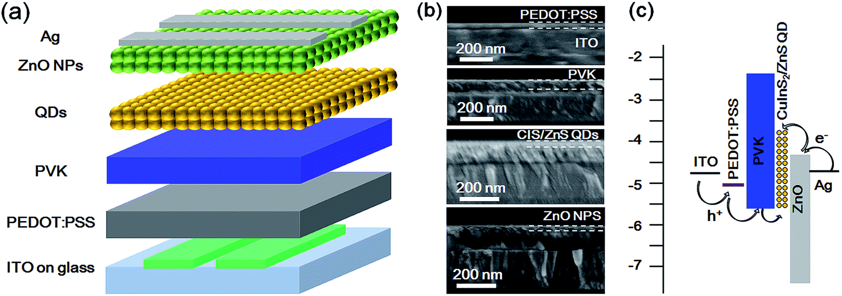 | ||
| Fig. 3 (a) Structure schematic of a CIS-based QLED and (b) cross-sectional SEM images taken after each layer is sequentially deposited. (c) Energy band diagram of CIS-based QLEDs. | ||
It is worth noting that the thicknesses of PVK and ZnO layers are crucial parameters to fabricate a high performance QLED. For the ETL layer, an excessively thick PVK layer easily results in a high turn-on voltage, while a thin layer more likely will weaken the blocking function of PVK and consequently leads to a low exciton-recombination efficiency at the QD layer region. So an appropriate PVK layer thickness of 45 nm is adopted herein. However, the opposite thickness-dependence is observed for the electronic properties of ZnO EHT. More specifically, by inferring from the electron-only device measurement we find that the ability of electron injection to QDs layer is enhanced when we thicken the ZnO layer, which completely differs with that of the HTL. The effect of ZnO thickness on voltage–current characteristics in electron-only devices can be seen in Fig. S3.† This unique property may be ascribed to the reduced resistance, which is similar to that rule for the ITO layer. Therefore, a 30 nm-thick ZnO layer is adopted which is partly required for the hole-blocking function and to reduce electrons that are injected to the QD layer, since the hole-current is proved in the following section to be much lower compared with the electron-current.
The spin-coated layers of PEDOT:PSS, PVK, ZCIS QDs and ZnO NPs are uniform and smooth, as can be seen in Fig. 4. AFM images reveal the root-mean-square roughness (RMS) values of each layer surface are 1.42 nm, 0.97 nm, 4.35 nm and 4.84 nm, respectively, indicating the feasibility for preparing smooth thin films by all solution processing.
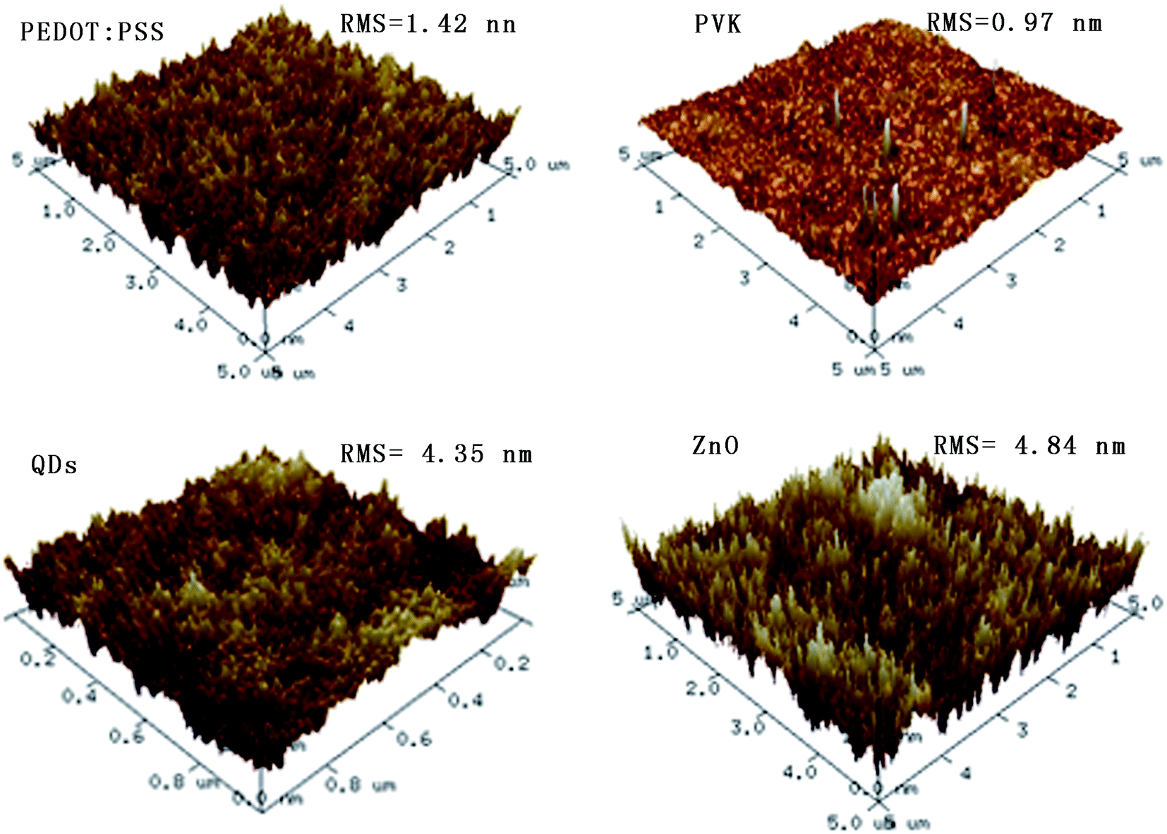 | ||
| Fig. 4 Pseudo-three-dimensional AFM images of PEDOT:PSS, PVK, QDs, and ZnO layers. The corresponding surface roughnesses for these layers are 1.42 nm, 0.97 nm, 4.35 nm and 4.84 nm, respectively. | ||
Fig. 5a presents voltage-dependent variations of luminance and current density of QLEDs having ZCIS QDs with different ligand surfaces. For QLEDs using DDT as the EML (DDT-QLEDs), a maximum luminance of 1067 cd m−2 was obtained under the voltage of 9.5 V. By contrast, a significant enhancement on luminescence in a practicable brightness region is found in EHT-QLEDs. The maximum luminescence for ZCIS-EHT QD-based devices (EHT-QLEDs) reaches up to 2354 cd m−2 at about 8.2 V. Besides, the EHT-QLEDs exhibit a lower turn-on voltage (defined by L0 > 1 cd m−2) of approximately 2.7 V as compared with that of DDT-QLEDs (∼3.1 eV). This low turn-on voltage is much lower than those reported in the literature (>3.7 V).32–34 At a given voltage above the threshold voltage, the device with ZCIS-EHT QDs has a slightly higher current density than the device with ZCIS-DDT QDs, which qualitatively confirms the reduction of the energy barrier for carrier injection to the ZCIS-EHT QD emitting layer.34,41 Fig. 5b depicts the voltage dependence of current efficiency and EQE for these two QLEDs. A maximum current efficiency of 0.41 cd A−1 is obtained, and is approximately 2-fold higher than that in DDT-QLEDs (0.15 cd A−1). A similar tendency is observed in EQE measurements. The maximum EQE in DDT-QLEDs is only ∼0.32% while that for EHT-QLEDs has increased to 0.63%, which is mainly due to the enhancement of the hole injection from the HTL to the QD layer and consequently leads to a higher exciton recombination efficiency in devices. Note that under high driving voltages (>8 V), other efficiency loss mechanisms such as field- or charge-induced exciton dissociation may further limit the quantum efficiency.42 Fig. 5c compares the maximum EQE for QLEDs using different ligand QDs as emitting materials. 64 samples are prepared and tested for drawing this histogram. The DDT-QLEDs exhibit the maximum EQE ranging from 0.25% to 0.50%. Better yet, EHT-QLEDs possess a maximum EQE distribution from 0.40% to 0.63%, suggesting the reproducibility of high performance of EHT-QLEDs.
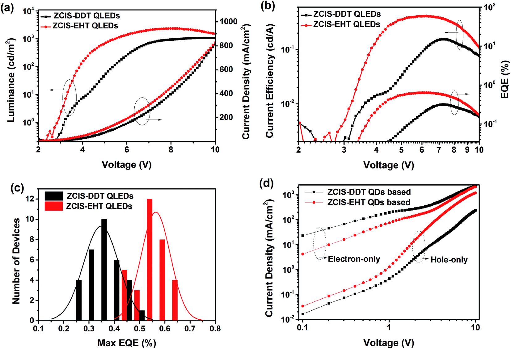 | ||
| Fig. 5 (a) Current density and luminance of the devices based on QDs with DDT and EHT ligands as a function of driving voltage. (b) Voltage-dependent variations of luminous efficiency and external quantum efficiency of QLEDs based on ZCIS QDs with different surface ligands. (c) Statistical histogram of maximum external quantum efficiency, tested from 32 devices for each kind of QLED. (d) Current density–voltage characteristic curves based on single-carrier devices using ZCIS-DDT and ZCIS-EHT QDs as the interlayer. | ||
To obtain deep insight into the mechanism of this performance improvement, it is important to compare the carrier injection/transport properties in devices with the use of ZCIS-QDT and ZCIS-EHT QDs. Therefore, single carrier devices with only electrons or holes migrating through QDs are fabricated and characterized. The electron-only devices are designed based on a multilayer structure (see Fig. S4a†) of ITO/ZnO (30 nm)/QDs (30 nm)/ZnO (30 nm)/Ag (120 nm), where the two ZnO ETL layers prevent the hole injection from electrodes (see Fig. S4b† for schematic energy level diagrams). Similarly, hole-only devices (structure shown in Fig. S4c†) consisting of ITO/PEDOT:PSS (35 nm)/PVK (45 nm)/QDs (25 nm)/PVK (45 nm)/Ag (120 nm) are fabricated. In these hole-only devices, the current–voltage curve characterizes the hole transport behavior of devices because electrons are blocked by the PVK layer (see Fig. S4d in ESI†). From the single-carrier device characteristics shown in Fig. 5d, we conclude that the electron current dominates the hole current at typical voltage range of 0–10 V. In the case of ZCIS-DDT QDs serving as the emitting layer, the disparity for electron and hole currents is about one (at high voltage) to three (at low voltage) orders of magnitude. So the low quantum efficiency could be ascribed to the imbalance of electron and hole injections. The ligand exchange from DDT to EHT, however, leads to a much higher increase in the hole current and simultaneously a significant drop of electron current, which enables a relative carrier balance and hence an improved device performance. As reported in other literature,34,41 a short ligand chain can significantly reduce the barrier thickness for hole injection to the QDs and thereby lead to an increase of hole current. Besides, the decrease of electron current is more likely related to the reduction of electron-donating groups (CH2) in ligands. As can be seen in Fig. 5d, the minimum disparity of electron and hole current occurs at ∼8 V in ZCIS-EHT QD-based single-carrier devices, which is in qualitative agreement with the experimental observation in maximum EQE of QLEDs. As a whole, the improvement on device performance is attributed to the relative electron–hole current balance in these EHT-QLEDs.
The EL spectra of CIS-based QLEDs in our study are given in Fig. 6a. Compared with the PL spectrum shown in Fig. 2d (PL peak at 560 nm), the EL for CIS-based QLEDs exhibits a ∼13 nm red-shift (EL peak is located at 573 nm), which is due to the dielectric function of the surrounding medium and/or the energy transfer from small to large QDs in the ensemble.43–46 Meanwhile, the EL bandwidth becomes broader in a higher voltage. This spectral broadening can be ascribed to a larger exciton polarization under a higher electric field, resulting in the increased LO (longitudinal optical)-phonon coupling.47 Even so, our devices exhibit a stable EL color with increasing voltage which is prepotent over conventional QLEDs that usually red-shift with increasing voltage due to the so-called quantum confined Stark effect (QCSE).47 The EL images at different voltages are also illustrated in Fig. 6a and the corresponding Commission Internationale de l’Eclairage (CIE) coordinates are given in Fig. 6b. Notably, the color of our QLEDs defined by CIE coordinate remains unchanged (0.45, 0.54) with increasing voltage, which is consistence with the results of EL spectra. In addition, the evolution of the EL spectra during a prolonged use with a constant current (100 mA cm−2) is measured. It can be observed that the EL peak location in Fig. 6c kept stable which also verifies the color retainability of our devices. Fig. 6d depicts the lifetime of QLEDs using different surface ligand of ZCIS QDs. The unpackaged EHT-QLEDs show a better stability compared with the DDT-QLEDs. This could be also ascribed to the improvement of charge unbalance after adopting a ligand exchange process which has been sufficiently demonstrated by Dai.14
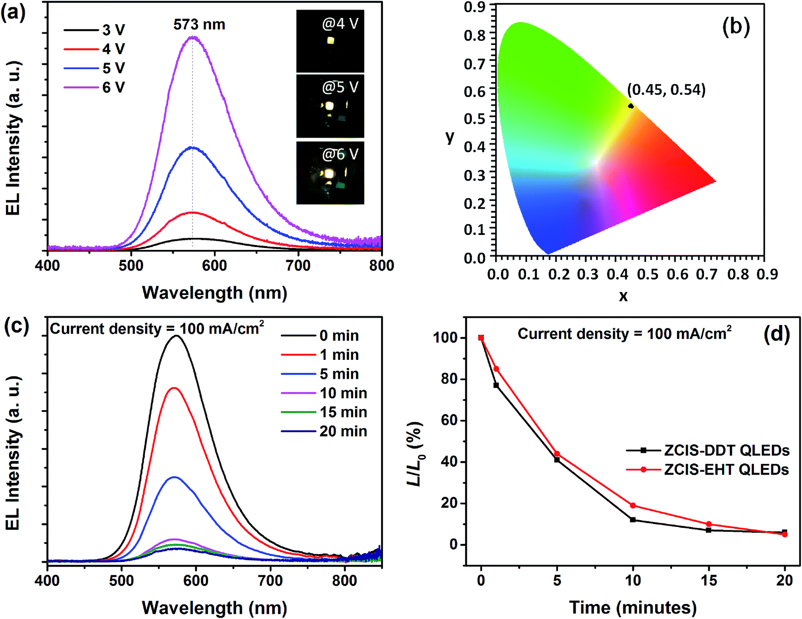 | ||
| Fig. 6 (a) Evolution of EL spectra of a yellow QLED with increasing voltage from 3 V to 6 V. The insets are the EL images of the QLED under applied voltages of 4 V, 5 V and 6 V, respectively. (b) CIE color coordinates of (0.45, 0.54) corresponding to the yellow EL spectra in (a). (c) EL spectra evolution with increasing usage time at 100 mA cm−2 current density condition. (d) Stability data for QLEDs (L, luminance). The device was tested at ambient conditions (temperature, 25 °C; relative humidity, 65%, unpackaged). | ||
4. Conclusions
In summary, multilayer CIS-based QLEDs that exhibit high luminescence, solution processability and color retainability are reported. A significant improvement on device performance is demonstrated using EHT-capped QDs as emitting materials. The EHT-QLEDs exhibit a maximum luminance of 2354 cd m−2 and an external quantum efficiency of 0.63%. With the reduction of energy barrier for holes injecting to the QD layer, the turn-on voltage of QLEDs decreases from 3.1 V to 2.7 V. Besides, these CIS-based QLEDs have an advantage of color retainability at various operating voltages. The strategy of ligand exchange can be extended to improve hybrid QLEDs with other types of QD emitters, and this study on QLED fabrication discussed above may offer a practicable platform for further research, leading to the achievement of all-solution processed, low-cost, low-toxicity and efficient QLEDs.Acknowledgements
This work was supported by the National Natural Science Foundation of China (projects 21073193 and 21273241), Project on the Integration of Industry, Education and Research of Guangdong Province (2012B091100476), Science and Technology Research Project of Guangzhou City (2014J4100218), Open Fund of Jiangsu Key Laboratory of Materials and Technology for Energy Conversion (MTEC-2015M01) and Natural Science Foundation of Guangdong Province (2015A030310501).References
- X. J. Xu, L. F. Hu, N. Gao, S. X. Liu, S. Wageh, A. A. Al-Ghamdi, A. Alshahrie and X. S. Fang, Adv. Funct. Mater., 2015, 25, 445–454 CrossRef CAS.
- K. Boldt, C. Ramanan, A. Chanaewa, M. Werheid and A. Eychmuller, J. Phys. Chem. Lett., 2015, 6, 2590–2597 CrossRef CAS PubMed.
- J. S. Steckel, J. P. Zimmer, S. Coe-Sullivan, N. E. Stott, V. Bulovic and M. G. Bawendi, Angew. Chem., Int. Ed., 2004, 43, 2154–2158 CrossRef CAS PubMed.
- B. L. Wu, H. J. Chao, C. P. Chen, C. H. Yang and J. Y. Chang, RSC Adv., 2015, 5, 36605–36613 RSC.
- J. Y. Pan, J. Chen, Q. Q. Huang, Q. Khan, X. Liu, Z. Tao, W. Lei, F. Xua and Z. C. Zhang, RSC Adv., 2015, 5, 82192–82198 RSC.
- W. H. Zhou, J. Jiao, Y. Zhao, X. Y. Cheng, D. X. Kou, Z. J. Zhou and S. X. Wu, RSC Adv., 2014, 4, 7617–7622 RSC.
- A. Castan, H. M. Kim and J. Jang, ACS Appl. Mater. Interfaces, 2014, 6, 2508–2515 CAS.
- Z. Yang, O. Voznyy, M. Liu, M. Yuan, A. H. Ip, O. S. Ahmed, L. Levina, S. Kinge, S. Hoogland and E. H. Sargent, ACS Nano, 2015, 9, 12327–12333 CrossRef CAS PubMed.
- H. Zhang, H. Li, X. Sun and S. Chen, ACS Appl. Mater. Interfaces, 2016, 8, 5493–5498 CAS.
- S. Y. Liu, H. Zhang, Y. Qiao and X. G. Su, RSC Adv., 2012, 2, 819–825 RSC.
- N. Kim, W. Na, W. Yin, H. Jin, T. K. Ahn, S. M. Cho and H. Chae, J. Mater. Chem. C, 2016, 4, 2457–2462 RSC.
- V. L. Colvin, M. C. Schlamp and A. P. Alivisatos, Nature, 1994, 370, 354–357 CrossRef CAS.
- J. Kwak, W. K. Bae, D. Lee, I. Park, J. Lim, M. Park, H. Cho, H. Woo, Y. Yoon do, K. Char, S. Lee and C. Lee, Nano Lett., 2012, 12, 2362–2366 CrossRef CAS PubMed.
- X. Dai, Z. Zhang, Y. Jin, Y. Niu, H. Cao, X. Liang, L. Chen, J. Wang and X. Peng, Nature, 2014, 515, 96–99 CrossRef CAS PubMed.
- K. H. Lee, J. H. Lee, H. D. Kang, B. Park, Y. Kwon, H. Ko, C. Lee, J. Lee and H. Yang, ACS Nano, 2014, 8, 4893–4901 CrossRef CAS PubMed.
- L. Qian, Y. Zheng, J. G. Xue and P. H. Holloway, Nat. Photonics, 2011, 5, 543–548 CrossRef CAS.
- H. Lee, C. M. Kang, M. Park, J. Kwak and C. Lee, ACS Appl. Mater. Interfaces, 2013, 5, 1977–1981 CAS.
- L. De Trizio, M. Prato, A. Genovese, A. Casu, M. Povia, R. Simonutti, M. J. P. Alcocer, C. D’Andrea, F. Tassone and L. Manna, Chem. Mater., 2012, 24, 2400–2406 CrossRef CAS.
- B. Mao, C.-H. Chuang, J. Wang and C. Burda, J. Phys. Chem., 2011, 115, 8945–8954 CAS.
- D. Aldakov, A. Lefrançois and P. Reiss, J. Mater. Chem. C, 2013, 1, 3756 RSC.
- Y.-K. Kim, S.-H. Ahn, K. Chung, Y.-S. Cho and C.-J. Choi, J. Mater. Chem., 2012, 22, 1516–1520 RSC.
- K. Gugula, L. Stegemann, P. J. Cywinski, C. A. Strassert and M. Bredol, RSC Adv., 2016, 6, 10086–10093 RSC.
- W. Zhang, Q. Lou, W. Ji, J. Zhao and X. Zhong, Chem. Mater., 2014, 26, 1204–1212 CrossRef CAS.
- D. Deng, Y. Chen, J. Cao, J. Tian, Z. Qian, S. Achilefu and Y. Gu, Chem. Mater., 2012, 24, 3029–3037 CrossRef CAS.
- R. Xie, M. Rutherford and X. Peng, J. Am. Chem. Soc., 2009, 131, 5691–5697 CrossRef CAS PubMed.
- B. Chen, H. Zhong, W. Zhang, Z. a. Tan, Y. Li, C. Yu, T. Zhai, Y. Bando, S. Yang and B. Zou, Adv. Funct. Mater., 2012, 22, 2081–2088 CrossRef CAS.
- W. S. Song and H. Yang, Chem. Mater., 2012, 24, 1961–1967 CrossRef CAS.
- X. Yuan, J. Hua, R. Zeng, D. Zhu, W. Ji, P. Jing, X. Meng, J. Zhao and H. Li, Nanotechnology, 2014, 25, 435202 CrossRef PubMed.
- P. H. Chuang, C. C. Lin and R. S. Liu, ACS Appl. Mater. Interfaces, 2014, 6, 15379–15387 CAS.
- A. Aboulaich, M. Michalska, R. Schneider, A. Potdevin, J. Deschamps, R. Deloncle, G. Chadeyron and R. Mahiou, ACS Appl. Mater. Interfaces, 2014, 6, 252–258 CAS.
- S. Cao, W. Y. Ji, J. L. Zhao, W. Y. Yang, C. M. Li and J. J. Zheng, J. Mater. Chem. C, 2016, 4, 581–588 RSC.
- Z. Tan, Y. Zhang, C. Xie, H. Su, J. Liu, C. Zhang, N. Dellas, S. E. Mohney, Y. Wang, J. Wang and J. Xu, Adv. Mater., 2011, 23, 3553–3558 CrossRef CAS PubMed.
- J.-H. Kim, C.-Y. Han, K.-H. Lee, K.-S. An, W. Song, J. Kim, M. S. Oh, Y. R. Do and H. Yang, Chem. Mater., 2015, 27, 197–204 CrossRef CAS.
- Z. Bai, W. Ji, D. Han, L. Chen, B. Chen, H. Shen, B. Zou and H. Zhong, Chem. Mater., 2016, 28, 1085–1091 CrossRef CAS.
- X. Wang, Z. Liang, X. Xu, N. Wang, J. Fang, J. Wang and G. Xu, J. Alloys Compd., 2015, 640, 134–140 CrossRef CAS.
- A. Lefrancois, B. Luszczynska, B. Pepin-Donat, C. Lombard, B. Bouthinon, J. M. Verilhac, M. Gromova, J. Faure-Vincent, S. Pouget, F. Chandezon, S. Sadki and P. Reiss, Sci. Rep., 2015, 5, 7768 CrossRef CAS PubMed.
- K. H. Lee, J. H. Lee, W. S. Song, H. Ko, C. Lee, J. H. Lee and H. Yang, ACS Nano, 2013, 7, 7295–7302 CrossRef CAS PubMed.
- J. Y. Pan, J. Chen, Q. Q. Huang, Q. Khan, X. Liu, Z. Tao, Z. C. Zhang, W. Lei and A. Nathan, ACS Photonics, 2016, 3, 215–222 CrossRef CAS.
- W. Ki Bae, J. Kwak, J. Lim, D. Lee, M. Ki Nam, K. Char, C. Lee and S. Lee, Nanotechnology, 2009, 20, 075202 CrossRef PubMed.
- H. Shen, X. Bai, A. Wang, H. Wang, L. Qian, Y. Yang, A. Titov, J. Hyvonen, Y. Zheng and L. S. Li, Adv. Funct. Mater., 2014, 24, 2367–2373 CrossRef CAS.
- H. Shen, W. Cao, N. T. Shewmon, C. Yang, L. S. Li and J. Xue, Nano Lett., 2015, 15, 1211–1216 CrossRef CAS PubMed.
- D. Bozyigit, O. Yarema and V. Wood, Adv. Funct. Mater., 2013, 23, 3024–3029 CrossRef CAS.
- Q. Sun, Y. A. Wang, L. S. Li, D. Y. Wang, T. Zhu, J. Xu, C. H. Yang and Y. F. Li, Nat. Photonics, 2007, 1, 717–722 CrossRef CAS.
- J. L. Zhao, J. A. Bardecker, A. M. Munro, M. S. Liu, Y. H. Niu, I. K. Ding, J. D. Luo, B. Q. Chen, A. K. Y. Jen and D. S. Ginger, Nano Lett., 2006, 6, 463–467 CrossRef CAS PubMed.
- P. O. Anikeeva, J. E. Halpert, M. G. Bawendi and V. Bulovic, Nano Lett., 2009, 9, 2532–2536 CrossRef CAS PubMed.
- W. K. Bae, J. Kwak, J. W. Park, K. Char, C. Lee and S. Lee, Adv. Mater., 2009, 21, 1690–1694 CrossRef CAS.
- V. Wood, M. J. Panzer, J. M. Caruge, J. E. Halpert, M. G. Bawendi and V. Bulovic, Nano Lett., 2010, 10, 24–29 CrossRef CAS PubMed.
Footnote |
| † Electronic supplementary information (ESI) available. See DOI: 10.1039/c6ra14241a |
| This journal is © The Royal Society of Chemistry 2016 |