
Bis(diphenylamino)naphthalene host materials: careful selection of the substitution pattern for the design of fully solution-processed triple-layered electroluminescent devices†
Frédéric Dumur*ab,
Thanh-Tuân Bui*c,
Sébastien Péraltac,
Marc Lepeltierd,
Guillaume Wantzbe,
Gjergji Sinic,
Fabrice Goubardc and
Didier Gigmesa
aAix-Marseille Université, CNRS, Institut de Chimie Radicalaire ICR, UMR 7273, F-13397 Marseille, France. E-mail: frederic.dumur@univ-amu.fr
bCNRS, IMS, UMR 5218, F-33400 Talence, France
cLaboratoire de Physicochimie des Polymères et des Interfaces, Université de Cergy-Pontoise, 5 mail Gay Lussac, 95000 Neuville-sur-Oise, France. E-mail: tbui@u-cergy.fr
dInstitut Lavoisier de Versailles, UMR 8180 CNRS, Université de Versailles Saint-Quentin en Yvelines, 45 avenue des Etats-Unis, 78035 Versailles Cedex, France
eBordeaux INP, IMS, UMR 5218, F-33400 Talence, France
First published on 16th June 2016
Abstract
Two new triarylamine-based wide bandgap small molecules differing by the position of their substituents were investigated as hosts for solution-processed organic light-emitting diodes (OLEDs). Blue-green, green and red OLEDs were realized with FIrpic, Ir(ppy)2(acac) and Ir(ppy)2(dbm) as triplet emitters respectively and the three layers constituting the device stacking were successively deposited with orthogonal solvents. Interestingly, one of the two bis(diphenylamino)naphthalene-based compounds, (NAP-1,5-DPA), furnished significantly enhanced EL performances compared to its isomeric counterpart. A maximum luminance of 3905 cd m−2 at 21 V was notably achieved with this material for devices comprising FIrpic as dopant. To get a deeper insight into these major differences in devices, the two host materials were characterized by UV-visible absorption and luminescence spectroscopy, and cyclic voltammetry. Thin films of the two materials were also examined by optical and atomic force microscopy. Thermal properties of the two hosts were also investigated as well as their electronic characteristics by theoretical calculations.
1. Introduction
During the past decades, a great deal of effort has been devoted to developing highly emissive organic light-emitting diodes (OLEDs).1–3 In this regard, phosphorescent emitters clearly outperform their fluorescent analogues. By harvesting both singlet and triplet excitons for light emission, a theoretical internal quantum efficiency of 100% can be achieved, contrarily to the intrinsic limitation of 25% observed for the fluorescent emitters.4 However, in 2013, Adachi et al. broke the 25% theoretical efficiency limit by use of thermally activated delayed fluorescence (TADF) emitters.5,6 Beyond the simple aspect of the light-emitting materials used to fabricate OLEDs, the way how devices are elaborated is another major concern. Depending of the materials, two approaches can be carried out. When polymers are used, solution processes such as spin-coating or inkjet-printing can be utilized to form layers.7 Conversely, for small molecules, the standard method consists in the thermal evaporation of the materials as these latter exhibit a strong propensity to crystallize. Therefore, a great deal of efforts has been devoted to develop small-molecule materials allowing the fabrication of OLEDs by solution-process and addressing the crystallization issue.8–19 Unlike polymers, small molecules combine the merits of a higher purity than polymers, an easier purification than polymers that ensures a well-controlled and reproducible purity, a minimal variation between synthesized samples, a well-defined structure and a precise molecular weight.20,21 As main advantages of the solution process, composition of the active layer can be easily tuned and more precisely controlled than during the co-evaporation of the host and the guest where a variation of the concentration in the bulk can still occur as a result of an inconstant deposition rate. As drawback, one major limitation exists, namely, the adverse dissolution of the previously coated layers by the solvent used to deposit the subsequent ones.22 The fabrication of multilayered devices is not trivial and several strategies have been developed to provide to the under layers the sufficient resistance to the solvent of the upper ones. Notably, in the crosslinking approach, the material is modified with a crosslinkable group and subsequent to its deposition, a thermal or photochemical treatment of the layer is applied to generate a crosslinked network structure that insolubilizes the material.23–25 Solution-processing of the next layer is then possible but this approach is limited to homemade materials as a chemical modification of the molecule is required prior use. Without recourse to crosslinking and applicable to benchmark materials, the concept of orthogonal solvents is easier to implement. To deposit the upper layer without washing out the previous ones, the material of the new layer has to be dissolved in a solvent that does not alter any materials of the under layers.26–28 This strategy is typically developed for all devices comprising PEDOT:PSS as the hole-injection layer. This water-soluble material widely used for its high conductivity and sufficient transparency in the visible region is also insoluble in organic solvents and allows the use of organic solvent-based inks to deposit the next layers.29–32 Parallel to this, materials classically used to form the emissive layer are often poorly soluble in highly polar solvents and erosion of the underlying hole-injection layer by deposition of the active layer is precluded.33 Conversely, the electron-transport material 1,3,5-tris(2-N-phenylbenzimidazolyl)benzene (TPBI) is soluble in alcohols.34 Therefore, by alternating the proper use of highly polar and less polar solvents, a sufficient solvent resistance is provided to allow the design of multilayered solution-processed devices. With regards to small-molecular hosts, triphenylamine-based materials have been less investigated than their carbazole analogues,35 especially as single host materials.36–40 Popularity of the carbazole moiety as building-block for the design of small molecule soluble host materials certainly arises from its remarkable properties such as a wide bandgap,41,42 a high triplet energy level,43–45 and a remarkable thermal, chemical and photochemical stability.46–52 However, triphenylamine only differs from carbazole by its unbonded aromatic rings and its non-planar structure. High hole mobility and low ionization potential of this group make it an excellent candidate for the design of host materials.53–56 So far, only few host materials with triphenylamine moieties have been reported.57,58 In this work, two molecules i.e. 1,5-bis(di(4-methoxyphenyl)amino)naphthalene (NAP-1,5-DPA) and 2,6-bis(di(4-methoxyphenyl)amino)naphthalene (NAP-2,6-DPA) have been investigated for the first time as hosts for OLEDs (see Fig. 1). More precisely, fully solution-processed triple-layer devices were fabricated by a careful selection of materials and orthogonal solvents. Interestingly, if the two isomers only differ by the linking topology between the peripheral bis(4-methoxyphenyl)amine and the central naphthalene unit, as it could anticipated, this modification endowed inequal host ability to the two materials and devices exhibiting the best characteristics were fabricated with NAP-1,5-DPA. To get a deeper insight in this behavior, the thermal, photophysical and electrochemical properties of NAP-1,5-DPA and NAP-2,6-DPA were investigated. We also demonstrated the applicability of these two materials as hosts for blue-green, green and red phosphorescent OLEDs. | ||
| Fig. 1 Structure of the two host materials investigated in this study. | ||
2. Experimental
2.1. General information
All used chemicals and solvents were purchased from chemical companies and used as received, unless otherwise mentioned. Toluene was dried by distillation from sodium metal. NMR (1H & 13C) spectra were recorded on a Bruker DPX-250 FT-NMR spectrometer. Chemical shifts are given in ppm using the residual solvent signal as internal reference (DMSO-d6, 2.50 ppm). UV-vis spectra were measured on a Jasco (V-570) UV-vis-NIR spectrophotometer. The fluorescence spectra were recorded in THF using a Jasco FP 6200 spectrometer. Thermogravimetric analysis (TGA) was carried out on a TA Instrument Q50 TGA under argon flow at a heating rate of 20 °C min−1. The temperature of thermal degradation (Td) was measured at the point of 5% weight loss. Differential scanning calorimetry (DSC) was performed on a TA Instruments Q100 calorimeter, calibrated with indium and flushed with argon. The electrochemical properties of the investigated compounds were measured in dichloromethane by cyclic and differential pulse voltammetries, with tetrabutylammonium hexafluoro-phosphate (0.1 M) as a supporting electrolyte in a standard one-compartment, three-electrode electrochemical cell under an argon stream using a VSP BioLogic potentiostat. The working, reference and counter electrodes were platinum disk (Ø = 1 mm), platinum wire pseudo-reference, and gold electrodes, respectively. Ferrocene was added at the end of each series of experience as an internal standard, and the potentials were referred to the reversible formal potential of this compound. Absolute fluorescence quantum yields were measured by a Hamamatsu Photonics Quantaurus QY at room temperature. The optical microscopy was acquired on a BX50 from Olympus and captured by Ueye camera from IDS. Atomic force microscopy (AFM) experiments were performed in ScanAsyst mode with a Nanoscope V controler coupled at Icon microscope from Bruker.2.2. Syntheses of NAP-1,5-DPA and NAP-2,6-DPA
General procedure for the synthesis of NAP-1,5-DPA and NAP-2,6-DPA: in a dry schlenk under argon stream, dibromo-naphthalene (1.16 mmol), bis(4-methoxyphenyl)amine (2.55 mmol), palladium(II) acetate (0.116 mmol), sodium tert-butoxide (4.64 mmol), tri-tert-butylphosphine (0.232 mmol, dissolved in 3 mL of toluene) and anhydrous toluene (12 mL) were charged. The septum-sealed schlenk was evacuated and refilled with argon five times. The mixture was stirred under an argon atmosphere in sealed Schlenk tube at 105 °C for 100 h. After cooled down to room temperature, the mixture was diluted with CH2Cl2 (100 mL) and filtered through a pad of silica gel. The filtrate was washed with brine and water, dried over anhydrous MgSO4, filtered, and concentrated under reduced pressure to give a viscous oil (ca. 2–3 mL) which was then dropped into methanol (250 mL) with stirring. The precipitate was then filtered, rinsed widely with methanol to yield the title compounds as a yellowish powder.1,5-Bis(di(4-methoxyphenyl)amino)naphthalene (NAP-1,5-DPA): 80% yield.
1H NMR (DMSO-d6, δ/ppm): 7.85 (d, 2H, J = 8.5 Hz); 7.44 (t, 2H, J = 8.5 Hz); 7.22 (d, 2H, J = 7.0 Hz); 6.86 (br, 16H); 3.72 (s, 12H).
13C NMR (DMSO-d6, δ/ppm): 155.3; 142.2; 132.3; 123.0; 114.7; 55.1.
2,6-Bis(di(4-methoxyphenyl)amino)naphthalene (NAP-2,6-DPA): 77% yield.
1H NMR (DMSO-d6, δ/ppm): 7.52 (d, 2H, J = 8.75 Hz); 7.08 (br, 2H); 7.04–6.99 (m, 10H); 6.95–6.91 (m, 8H); 3.77 (s, 12H). 13C NMR (DMSO-d6, δ/ppm): 155.7; 141.0; 128.6; 126.3; 115.3; 55.6.
2.3. OLEDs fabrication and measurements
All materials except the two hosts and two triplet emitters used in the devices were purchased from Lumtec with the best purity available and used as received. Solution-processed OLEDs were fabricated onto cleaned indium tin oxide (ITO) glass substrates with sheet resistance of 10–12 Ω sq−1. Prior to organic layer deposition, the ITO substrates were successively washed with acetone, ethanol and isopropanol under ultrasonic for 15 min before surface treatment with UV-ozone plasma for 20 min. This was followed by coating a 40 nm thick layer of poly(ethylene dioxythiophene):poly(styrene sulfonic acid) (PEDOT:PSS) on the treated ITO sheets at 4000 rpm for 60 s. The film was baked at 120 °C for 30 min under reduced pressure and the substrates were loaded in a glove box. A solution of host (40 mg mL−1 in 1,2-dichlorobenzene) with bis(4,6-difluorophenylpyridinato)picolate iridium(III) (FIrpic) bis(2-phenylpyridine)(acetylacetonato)iridium(III) Ir(ppy)2(acac)59 or bis(2-phenylisoquinoline)(1,3-diphenylacetonato)iridium(III) Ir(piq)2(dbm)60,61 (20 mg mL−1 in chloroform) was spin-coated at 1000 rpm on top of the PEDOT:PSS/ITO coated glass substrate under ambient conditions from a mixture of the two solutions. Next, an electron-transport and hole-blocking layer of 1,3,5-tris(N-phenyl-benzimidizol-2-yl)benzene (TPBI) (20 mg mL−1 in methanol) was spin-coated at 1000 rpm on top of the emissive layer. Thermal annealing of the organic layers was thus carried out for 12 hours at 60 °C. Finally, a 1 nm-thick LiF layer and an 80 nm-thick aluminum cathode layer were successively deposited on the substrates in high vacuum environment through a shadow mask. The resulting devices had the following structure; ITO/PEDOT:PSS (40 nm)/host![[thin space (1/6-em)]](https://www.rsc.org/images/entities/char_2009.gif) :Ir (x wt%, 1000 rpm with x = 5, 10) (60–80 nm)/TPBI (30 nm)/LiF (1 nm)/Al (80 nm). The EL spectra, CIE coordinates, current–voltage and brightness–voltage characteristics of the devices were recorded with an External Quantum Efficiency Measurement System (model C9920-12) of Hamamatsu Photonics K.K. The device configuration and the chemical structures of the materials that were used in this work are presented in the Fig. 2.
:Ir (x wt%, 1000 rpm with x = 5, 10) (60–80 nm)/TPBI (30 nm)/LiF (1 nm)/Al (80 nm). The EL spectra, CIE coordinates, current–voltage and brightness–voltage characteristics of the devices were recorded with an External Quantum Efficiency Measurement System (model C9920-12) of Hamamatsu Photonics K.K. The device configuration and the chemical structures of the materials that were used in this work are presented in the Fig. 2.
 | ||
| Fig. 2 Device configuration and formulas of the different materials used to fabricate OLEDs. | ||
2.4. Computational details
Density functional methods (DFT)62 by means of the B3LYP63,64 functional were used for the calculation of molecular properties. The geometry optimizations of the neutral molecules NAP-1,5-DPA and NAP-2,6-DPA were carried out without symmetry constraints at the 6-31G(d,p) level in “gas phase”. The vertical ionization potentials (Ip) were calculated at the neutral state geometry as energy difference between neutral and cation species. TD65–69 method was used for the calculation of the absorption spectra, the relaxation of the 1st singlet excited state in gas phase, and for the vertical and adiabatic triplet energy of each compound. Test calculations by using PBE0,70,71 and BMK72 functionals were performed in order to check for the reliability of the optical properties. The intramolecular reorganization energies (λi) of model compounds were calculated at the B3LYP-6-31G(d,p) level according to the following equation:73| λi = λi1 + λi2 = (Egeom(cation)N − Egeom(N)N) + (Egeom(N)cation − Egeom(N)cation) |
In this equation, Egeom(cation)N for instance corresponds to the energy of the neutral molecule (N) in the geometry of the cationic species (cation). All calculations were performed by using the Gaussian 09 program.74
3. Results and discussion
3.1. Synthesis of NAP-1,5-DPA and NAP-2,6-DPA
The synthetic routes toward different targeted molecules are outlined in Scheme 1. Both compounds were synthesized from commercially available dibromonaphthalene and di(4-methoxyphenyl)amine involving a classical twofold Pd-catalyzed Buchwald–Hartwig amination as established for similar compounds in our previous works.75–77 These final compounds were obtained as a yellowish powders in good yields (77–80%) after purification. As expected, all compounds have good solubility in common organic solvents (dichloromethane, chloroform, chlorobenzene, toluene, etc.) rendering them suitable for solution processed organic electronic devices.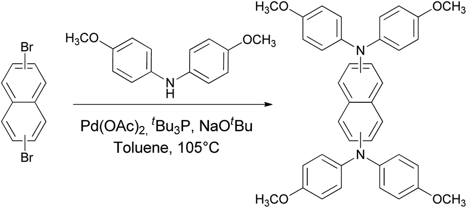 | ||
| Scheme 1 Synthetic route to NAP-1,5-DPA and NAP-2,6-DPA. | ||
3.2. Geometries and electronic properties
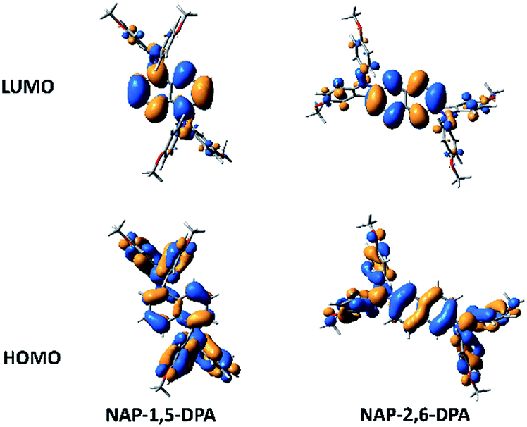
The structures of compounds NAP-1,5-DPA and NAP-2,6-DPA are shown in Fig. 3. The two N–C(Ph) bonds of a given diphenylamine (DPA) group exhibit dihedral angles with the naphthalene moiety (C(Ph)–N–C–C) of 66° and 49° in the case of NAP-1,5-DPA and 33° and 42° in NAP-2,6-DPA (averages of 57° and 39° respectively). The larger values for the 1,5 isomer are due to the stronger hindrance between one of the DPA phenyl groups with the naphthalene moiety. Highest Occupied Molecular Orbital (HOMO) and Lowest Unoccupied Molecular Orbital (LUMO) of compounds NAP-1,5-DPA and NAP-2,6-DPA are shown in Fig. 4. While both LUMOs are dominantly of naphthalene nature, the HOMOs show some differences: HOMO of NAP-1,5-DPA shows larger contribution from the DPA moieties, whereas HOMO of NAP-2,6-DPA shows slightly larger contribution from the naphthalene fragment. The increased contribution of the naphthalene fragment in HOMO of NAP-2,6-DPA seems to be due to the smaller DPA–naphthalene dihedral angles, in turn stemming from the smaller DPA–naphthalene steric hindrance in 2- and 6-positions as compared to 1- and 5-positions. | ||
| Fig. 3 Geometrical structures of compounds NAP-1,5-DPA and NAP-2,6-DPA (B3LYP/6-31G(d,p) level in “gas phase”). | ||
 | ||
| Fig. 4 HOMO and LUMO representations of compounds NAP-1,5-DPA and NAP-2,6-DPA (B3LYP/6-31G**). | ||
HOMO and LUMO energies are given in Table 1. Both levels are higher in NAP-2,6-DPA than in NAP-1,5-DPA. However, the evolution of HOMO energy is faster than for LUMO, so that the HOMO–LUMO gap is by 0.07 eV smaller for NAP-2,6-DPA as compared to NAP-1,5-DPA.
| Host materials | NAP-1,5-DPA | NAP-2,6-DPA | |
|---|---|---|---|
| a Onset oxidation potential versus ferrocene (Eonset vs. Fc).b Ionization potential Ip(CV) and electron affinity EA(CV) determined from the formulas: Ip(CV) = 4.8 + Eonset vs. Fc and EA(CV) = −(Ip(CV) − Eg(opt)).c Determined at the B3LYP-6-31G(d,p) level in gas phase.d Optical bandgap Eg(opt) estimated from the edge of the electronic absorption spectrum.e Quantum yield determined with an absolute quantum yield spectrometer.f Vertical triplet energy. | |||
| Tg (°C) | 73 | 58 | |
| Tcryst (°C) | 173 | 128 | |
| Tf (°C) | 187 | 227 | |
| Td (°C) | 346 | 335 | |
| Eonset (V)a | 0.01 | −0.24 | |
| Ip(CV) (eV)b | 4.81 | 4.56 | |
| EA(CV) (eV)b | 1.99 | 1.82 | |
| εLUMO (eV)c | −0.98 | −0.80 | |
| εHOMO (eV)c | −4.51 | −4.27 | |
| λonset (nm) | 439 | 453 | |
| Eg(opt) (eV)d | 2.82 | 2.74 | |
| λabs (nm)sol | 271, 290, 360, 381 | 278, 315, 346, 406 | |
| λem (nm, (eV))sol | 491 (2.53) | 454 (2.73) | |
| λabs (nm)solid | 310, 358, 388 | 314, 349, 411 | |
| λem (nm, (eV))solid | 463 (2.68) | 451 (2.75) | |
| ϕe | 0.48 | 0.44 | |
| S1/T1f/ΔEST (eV) | B3LYP | 2.94/2.30/0.65 | 2.97/2.31/0.66 |
| PBE0 | 3.08/2.23/0.85 | 3.06/2.26/0.80 | |
| BMK | 3.41/2.55/0.87 | 3.36/2.54/0.81 | |
The ground state (GS) dipole moments of these compounds were found to vary over a large range (0.1–3.8 D), due to the random orientation of the methoxy groups. However, for the same orientation of the OMe groups in both compounds, very similar dipole moments were found. The large distribution of the dipole moments is expected to negatively impact electron- and hole transport properties in the host materials. Additionally, much larger intramolecular reorganization energies were found for electron transport (0.51 eV and 0.49 eV for NAP-1,5-DPA and NAP-2,6-DPA respectively) than for holes (0.21 eV and 0.24 eV respectively). Based on Marcus' theory,78–80 strongly non-equilibrated electron- and hole transport in these materials could be predicted.
3.3. Electrochemical properties
Cyclic voltammetry has been employed to investigate the redox behavior of the two hosts and estimate their ionization potentials (IPs) and electron affinities (EAs). IPs and EAs were estimated by using the ferrocene (Fc) ionization potential value (4.8 eV vs. vacuum) as the standard. Their cyclic voltammograms are shown in Fig. 5 and relevant data are summarized in Table 1. Both compounds showed three electrochemical processes assigned to the oxidation of the two amine moieties and the naphthalene core. The first quasi-reversible oxidation processes can be attributed to the formation of a radical cation on the amine moiety with onset oxidation potentials of approximately 0.01 and −0.24 V vs. Fc/Fc+ (Table 1) for NAP-1,5-DPA and NAP-2,6-DPA, respectively. The lower oxidation potential of NAP-2,6-DPA clearly evidenced its larger electron delocalization system as compared to NAP-1,5-DPA and these results are consistent with the aforementioned theoretical results. The IPs values determined from the oxidation onset potential values with respect to Fc/Fc+ decrease by 0.25 eV (from 4.81 to 4.56 eV respectively), which is consistent with the increase of HOMO energy by 0.24 eV in the same sense. | ||
| Fig. 5 Cyclic voltammograms of NAP-1,5-DPA and NAP-2,6-DPA recorded in TBAPF6/CH2Cl2 at a scan rate of 100 mV s−1. | ||
3.4. Optical properties
Optical properties of NAP-1,5-DPA and NAP-2,6-DPA were evaluated by theoretical calculations and by measuring the room-temperature absorption and photoluminescence (PL) spectra of NAP-1,5-DPA and NAP-2,6-DPA in CH2Cl2 (see Fig. 6). Photophysical characteristics of the two materials are summarized in the Table 1. | ||
| Fig. 6 UV-visible absorption and photoluminescence spectra of NAP-1,5-DPA and NAP-2,6-DPA in CH2Cl2. For PL measurements, excitation wavelengths were 375 nm for NAP-1,5-DPA and 405 nm for NAP-2,6-DPA. | ||
The absorption spectra of the two compounds in solution are significantly influenced by the substitution pattern. Notably, three absorption bands in the 250–325 nm region can be distinguished for the two materials, attributable to π–π* transitions on the diphenylamine and the naphthalene moieties. Peaks observed in the 340–450 nm region are assigned to a mixture of charge transfer (CT) and local-naphthalene electronic transitions (Fig. 7). However, the lowest energy band is mainly of CT character in the case of NAP-1,5-DPA, whereas the local-naphthalene transitions seem to be more prominent in the case of NAP-2,6-DPA. A bathochromic shift of this absorption band is observed for NAP-2,6-DPA, indicative of a higher electronic delocalization in this isomer. From the edge of their absorption spectra, optical bandgap of the two materials could be calculated and determined as being 2.82 and 2.74 eV for NAP-1,5-DPA and NAP-2,6-DPA respectively.
 | ||
| Fig. 7 Experimental and theoretical absorption spectra of compounds NAP-1,5-DPA and NAP-2,6-DPA. | ||
As revealed by the Fig. 6, the fluorescence maximum of NAP-1,5-DPA in dichloromethane appears at 491 nm and shows a red-shift compared to the emission of NAP-2,6-DPA which is detected at 454 nm. Very different Stokes shifts of 110 nm (0.72 eV) and 48 nm (0.32 eV) respectively were obtained, with a difference of 0.4 eV between them. In order to estimate the intramolecular contribution to the Stokes shifts, the S1 geometries of both compounds were optimized in gas phase. Larger intramolecular relaxation by roughly two times was found for NAP-1,5-DPA as compared to NAP-2,6-DPA (0.41 eV and 0.23 eV respectively), which is consistent with the decrease of Stokes shifts by roughly two times in the same order. The origin of this difference can be understood in terms of distributions of the frontier orbitals in these compounds. Indeed, given that the S0 → S1 transition exclusively involves the HOMO and LUMO orbitals, the principal difference between the two compounds resides in the different distributions of their HOMOs, being dominantly localized in the DPA fragments for NAP-1,5-DPA as compared to the naphthalene fragment for NAP-2,6-DPA (Fig. 4). Accordingly, the geometrical modifications subsequent to the HOMO → LUMO (dominantly CT) transition will be stronger in the case of NAP-1,5-DPA as compared to NAP-2,6-DPA (dominantly local-naphthalene transition), thus resulting in larger (intramolecular) Stokes shift in the former case. However, the difference between the intramolecular relaxations of NAP-1,5-DPA and NAP-2,6-DPA (Δ = 0.18 eV), which represents the contribution of the intramolecular part in the difference between the Stokes shifts, is by roughly two times smaller than the experimental value of 0.4 eV. The contribution of the solvent relaxation in the Stokes shifts in these compounds is consequently important. Our results obtained for the relaxed geometries of the S1 state indicate important dipole moment in the case of NAP-1,5-DPA (15 D), as opposed to the small S1 dipole moments for NAP-2,6-DPA (0.2 D, Table S1†). The much larger difference between the S1 and GS dipole moments (Δμ) in the case of NAP-1,5-DPA (∼15 D) as compared to NAP-2,6-DPA (0.1 D) is thus consistent with the smaller Stokes shift in the latter case.
Both solvent relaxation and intramolecular geometrical deformations are consequently more important in the case of NAP-1,5-DPA, thus explaining the larger Stokes shift for this compound as compared to NAP-2,6-DPA. These results seem to correlate with two geometrical differences between the two compounds: (i) a stronger increase in the DPA–naphthalene dihedral angles is observed during the relaxation of the S1 state in the case of NAP-1,5-DPA (from 57° to 78°, average values) as compared to NAP-2,6-DPA (from 39° to 55°). (ii) Importantly, the relaxed S1 geometry of NAP-1,5-DPA is asymmetric, with individual DPA–naphthalene dihedrals of 84° and 72°, as opposed to the identical ones for NAP-2,6-DPA. Accordingly, charge localization is expected in the case of NAP-1,5-DPA, being in the origin of the strong S1 dipole moment for NAP-1,5-DPA. Indeed, the calculation of the charges on each fragment in the S1 state (relaxed geometry) confirms the above suggestions, resulting in charges of −0.3e, −0.14e, and 0.44e for DPA, naphthalene, and DPA fragments respectively. The origin of this charge localization can be traced back to the poor naphthalene bridging in the HOMO of NAP-1,5-DPA (Fig. 4), in turn stemming from the important DPA–naphthalene steric hindrance in this compound.
In thin films state, a red-shift of the absorption spectra is observed for the two molecules, consistent with π–π stacking in the solid state. Anomalously, the emission spectra of NAP-1,5-DPA showed a marked blue-shift from 491 in solution to 463 nm in the solid state whereas only a slight blue-shift from 454 to 451 nm was observed for NAP-2,6-DPA (see Fig. 8), resulting in Stokes shifts of 75 nm (0.52 eV) and 40 nm (0.27 eV). Blue-shift of the emissions was assigned to the restricted conformational relaxation in the solid state.81–83 However, the decrease of the Stokes shift in the solid film of NAP-2,6-DPA as compared to solution is very small (8 nm, 0.05 eV), suggesting that the geometrical restrictions in the solid film are not important in this case. Additionally, the difference in GS versus S1 dipole moments is negligible for this compound (0.1 D, Table S1†), consistent with the very small decrease of the Stokes shift. On the contrary, the decrease of the Stokes shift in the solid film of NAP-1,5-DPA are much larger (35 nm, 0.21 eV). This important difference between the two compounds seems to principally stem from their difference in the S1 dipole moments (0.2 D and 15 D for NAP-2,6-DPA and NAP-1,5-DPA respectively), in correlation with the strong decrease in medium polarity from solution (ε = 8.93) to the solid films (dipole moments 0.1–0.5 D).
 | ||
| Fig. 8 UV-visible absorption and photoluminescence spectra of NAP-1,5-DPA and NAP-2,6-DPA in thin films. For PL measurements, excitation wavelength was 410 nm for the two materials. | ||
3.5. Thermal properties
To be of practical consideration for OLED fabrication, the two materials should form stable glasses. The thermal properties of the two new compounds were thus investigated by thermal gravimetric analyses (TGA) and differential scanning calorimetry (DSC). As anticipated, the introduction of tridimensional triphenylamine at both ends of the two molecules renders these structures non planar, what is strongly beneficial for the thermal stability of the materials. Decomposition temperatures (Td, which correspond to 5% weight loss) ranging from 335 to 346 °C were thus determined, evidencing the robustness of the two materials (see Fig. 9). | ||
| Fig. 9 TGA thermograms of NAP-1,5-DPA and NAP-2,6-DPA measured at a heating rate of 20 °C min−1 under an argon atmosphere. | ||
Glass-transition temperatures (Tg) of the two materials were also investigated (see Fig. 10). During the first heating cycle, NAP-1,5-DPA and NAP-2,6-DPA melted at 187 °C and 227 °C, respectively. Upon cooling from the melts, a crystallization occurred at 173 °C and 128 °C for NAP-1,5-DPA and NAP-2,6-DPA respectively, forming glassy states. In the subsequent heating cycles, a glass transition at 73 °C for NAP-1,5-DPA and 58 °C for NAP-2,6-DPA were determined. Based on these considerations, it can be concluded that the two materials are promising, from the point of view of their thermal stability, for applications into OLEDs.
 | ||
| Fig. 10 DSC curves of NAP-1,5-DPA and NAP-2,6-DPA (measurements at a heating rate of 20 °C min−1 under an argon atmosphere). | ||
It has to be noticed that NAP-2,6-DPA exhibits a relatively low Tg that remains however in the range of temperature observed for benchmark materials such as 4,4′-N,N′-dicarbazole-biphenyl (CBP) (62 °C) or 1,3-bis(9-carbazolyl)benzene (mCP) (60 °C).84,85
Therefore, this low Tg doesn't constitute a major impediment to elaborate devices with this material. To get a deeper insight into the physical properties of the two materials, optical characterizations of their respective thin films with/without dopant were carried out. Indeed, conjugated small molecules suffer from a strong tendency to crystallize, especially during the drying process that can adversely affect the uniformity of the resulting films and thus the device performances. For this study, we focused on the morphology of thin films comprising FIrpic as the dopant at three dopant concentrations (0, 5 and 10 wt%). To be representative of OLEDs later fabricated, thin films were deposited on the experimental conditions later used to elaborate OLEDs, with an active layer deposited on top of a PEDOT:PSS layer (see conditions in the Experimental section). As evidenced in the Fig. 11, optical micrographs of films showed major differences in the film morphology of the two materials. Thus, relatively uniform and smooth films only comprising discrete crystals of iridium complex were observed for NAP-1,5-DPA-based layers (see Fig. 11a–c). Conversely, NAP-2,6-DPA-based layers are characterized by extended domains comprising crystals of various sizes from both NAP-2,6-DPA and/or FIrpic (see Fig. 11d–f).
 | ||
| Fig. 11 Optical microscopy images of thins films after spin-coating with 1,2-dichloro-benzene of NAP-1,5-DPA (a) neat film (b) with 5 wt% FIrpic (c) with 10 wt% FIrpic and NAP-2,6-DPA (d) neat film (e) with 5 wt% FIrpic (f) with 10 wt% FIrpic at two different sizes. | ||
Presence of these domains are representative of a spontaneous nucleation of NAP-2,6-DPA during solvent evaporation, irrespective of the dopant concentration. From these results, it can already be anticipated that lower device performances can be attended from NAP-2,6-DPA-based devices compared to NAP-1,5-DPA-based devices. Following this initial study, surface profiles of thin films were examined at the nanometer scale by atomic force microscopy (AFM) (see Fig. 12). A visual inspection of the different AFM images of NAP-1,5-DPA and NAP-2,6-DPA-based films at different dopant concentrations revealed no significant changes in the surface topography. Films are characterized by a uniform granular structure with small surface undulations, indicative of a moderate roughness. For images 2 μm × 2 μm, the roughness (RMS) is between 0.34 and 0.44 nm.
 | ||
| Fig. 12 AFM images of NAP-1,5-DPA (a) neat film (b) with 5 wt% FIrpic (c) with 10 wt% FIrpic and NAP-2,6-DPA (d) neat film (e) with 5 wt% FIrpic (f) with 10 wt% FIrpic at different sizes (on the top: 2 μm × 2 μm, on the upper: 10 μm × 10 μm). | ||
3.6. Electroluminescence properties
To assess the utility of these materials as hosts for OLEDs, solution-processed devices were fabricated using FIrpic, Ir(ppy)2(acac) or Ir(ppy)2(dbm) as the blue-green, green and red dopants. Devices with the configuration of ITO/PEDOT:PSS (40 nm)/host:Ir complex (5–10 wt%, 1000 rpm)/TPBI (40 nm)/LiF (1 nm)/Al were prepared. Three layers were deposited by solution-process, namely the hole-injection layer (PEDOT:PSS in water), the active layer (in 1,2-dichlorobenzene) and the electron-transport layer (TPBI in methanol). More precisely, methanol was selected as solvent for TPBI as this solvent is a counter-solvent used to trigger the precipitation of NAP-1,5-DPA and NAP-2,6-DPA during their purification steps. Fig. 13 presents the current–voltage–luminance (J–V–L) characteristics and Fig. 14 shows the curves of current and power efficiencies versus current density for FIrpic-based devices. Noticeably, electroluminescence spectra of OLEDs consisted of the pure emission characteristic from the triplet emitters, without any residual emission from the host and/or the adjacent layers (see Fig. 15). At first sight, this result would suggest a good confinement of excitons within the emissive layer. However, the singlet energies of 2.68 eV and 2.75 eV deduced from the fluorescence (FL) spectra in solid films of NAP-1,5-DPA and NAP-2,6-DPA (Table 1) suggest even lower triplet energies. Indeed, our calculations of the exchange energy (ΔEST, Table 1) indicate triplet levels by 0.65 eV below the S1 level for both compounds. By arbitrary considering this last value as overestimated by roughly two times (due to the limited calculation level), and by making use of the FL singlet energies, triplet energies of roughly 2.30 eV and 2.35 eV can be estimated for NAP-1,5-DPA and NAP-2,6-DPA respectively. Compared to the triplet level of 2.65 eV of FIrpic, the estimated triplet levels of NAP-1,5-DPA and NAP-2,6-DPA should thus be lower in energy, which would constitute a loss channel for the triplet guest emission. Intriguingly, no reverse guest-to-host energy transfer is detected (Fig. 15), which could be explained by two opposite scenarios: (i) the first scenario assumes that the FL results in solid films of these compounds does not correspond to the real environment of the hosts in the host–guest mixtures. Indeed, due to the geometrical deformations and polarizations happening at the host–guest interface, shifting of the HOMO and LUMO levels generally occurs,86–88 which would result in increased S1 and T1 energies.
 | ||
| Fig. 13 Luminance–voltage characteristics obtained with NAP-1,5-DPA (a) and NAP-2,6-DPA (b) as hosts and FIrpic as the dopant. | ||
 | ||
| Fig. 14 Current and power (inset) efficiency vs. current density of OLEDs fabricated with NAP-1,5-DPA (top) and NAP-2,6-DPA (bottom) as hosts and FIrpic as the dopant. | ||
 | ||
| Fig. 15 Electroluminescence spectra of devices fabricated with NAP-1,5-DPA and NAP-2,6-DPA recorded at 50 mA cm−2. Inset: CIE coordinates of the emitted light. | ||
We speculate that these shifts reach the necessary values to avoid the reverse triplet guest → host transfer. However, the drawback of this phenomena would be that the lower (higher) HOMO (LUMO) level for the interfacial host molecules as compared to the “bulk” host molecules would also induce detrimental barriers for hole- and electron transfer from the “bulk” to the host–guest interface. (ii) The second scenario does not exclude the reverse guest → host triplet transfer. In order to explain the absence of any residual emission from the host and/or the adjacent layers (Fig. 15), we speculate that the triplet host levels could either decay nonradiatively, or return back to the guest by thermal activation (similar to TADF89). However, while the ΔEST values of the order of or larger than 0.3–0.4 eV would suggest small efficiency for the TADF-like mechanism, the guest → host reverse transfer followed by a nonradiative-decay scenario would be consistent with the very small device efficiencies of 1–2% (Table 2).
| Doping conc. (wt%) | Host | Vturn-ona (V) | CIE (x, y)b | λELc (nm) | L (cd m−2) | Current eff. (cd A−1) | Power eff. (lm W−1) | EQE (%) |
|---|---|---|---|---|---|---|---|---|
| a Turn-on voltage at a brightness of 1 cd m−2.b At maximum brightness.c Dominant wavelength at maximum brightness. | ||||||||
| FIrpic | ||||||||
| 5 | NAP-1,5-DPA | 9.2 | 0.18, 0.37 | 473 | 2570 (21 V) | 1.50 | 0.22 | 0.82 |
| 7 | NAP-1,5-DPA | 8.8 | 0.19, 0.37 | 474 | 3905 (21 V) | 1.51 | 0.23 | 0.84 |
| 10 | NAP-1,5-DPA | 8.8 | 0.18, 0.36 | 474 | 1650 (21 V) | 1.34 | 0.20 | 0.73 |
| 5 | NAP-2,6-DPA | 9.8 | 0.19, 0.34 | 472 | 586 (21 V) | 1.21 | 0.18 | 0.64 |
| 7 | NAP-2,6-DPA | 10.0 | 0.18, 0.38 | 473 | 748 (21 V) | 1.27 | 0.19 | 0.68 |
| 10 | NAP-2,6-DPA | 9.8 | 0.18, 0.37 | 473 | 419 (21 V) | 1.14 | 0.17 | 0.61 |
|
||||||||
| Ir(ppy)2(acac) | ||||||||
| 5 | NAP-1,5-DPA | 9.4 | 0.31, 0.62 | 519 | 6591 (21 V) | 1.38 | 0.15 | 0.79 |
| 7 | NAP-1,5-DPA | 9.4 | 0.33, 0.62 | 520 | 7222 (20.8 V) | 1.44 | 0.14 | 0.83 |
| 10 | NAP-1,5-DPA | 9.6 | 0.33, 0.62 | 520 | 5081 (20.6 V) | 1.44 | 0.16 | 0.83 |
| 5 | NAP-2,6-DPA | 10.0 | 0.34, 0.62 | 517 | 1420 (21 V) | 1.36 | 0.20 | 0.74 |
| 7 | NAP-2,6-DPA | 9.6 | 0.34, 0.61 | 518 | 1844 (21 V) | 1.42 | 0.21 | 0.77 |
| 10 | NAP-2,6-DPA | 9.4 | 0.34, 061 | 518 | 1669 (21 V) | 1.35 | 0.20 | 0.73 |
|
||||||||
| Ir(ppy)2(dbm) | ||||||||
| 5 | NAP-1,5-DPA | 13.2 | 0.66, 0.33 | 625 | 3674 (27.2) | 2.43 | 0.28 | 1.93 |
| 7 | NAP-1,5-DPA | 12.8 | 0.65, 0.32 | 625 | 3886 (27.4) | 2.70 | 0.31 | 2.07 |
| 10 | NAP-1,5-DPA | 13.6 | 0.66, 0.33 | 625 | 3040 (28.2) | 2.50 | 0.28 | 1.88 |
| 5 | NAP-2,6-DPA | 14.2 | 0.65, 0.34 | 626 | 1866 (27.8) | 1.50 | 0.17 | 0.92 |
| 7 | NAP-2,6-DPA | 14.0 | 0.65, 0.35 | 625 | 2204 (27.6) | 1.46 | 0.17 | 0.88 |
| 10 | NAP-2,6-DPA | 14.4 | 0.63, 0.34 | 625 | 1763 (27.6) | 1.13 | 0.13 | 0.57 |
According to the J–V–L curves recorded for the three triplet emitters, the two hosts exhibited unequal performances. Notably, performances of NAP-1,5-DPA-based devices were much better than those of NAP-2,6-DPA-based devices, irrespective of the dopant (see Table 2). Brightness of NAP-2,6-DPA-based devices was approximately divided by a factor of 5 compared to that of NAP-1,5-DPA-based devices while using FIrpic as the dopant. A factor of 3 and 2 were respectively determined for Ir(ppy)2(acac) or Ir(ppy)2(dbm). If a clear decrease of the maximum luminance was observed for NAP-2,6-DPA-based devices, current and power efficiencies were less affected as a result of a lower current measured for NAP-2,6-DPA-based devices.
As previously deduced from the aforementioned spectroscopic investigations (see Section 3.5), lower performances of NAP-2,6-DPA-based devices can be confidently assigned to an unfavorable morphology of the emissive layer. Notably, presence of numerous crystals within the emissive layer strongly contributes to generate defects and pathways for leakage current, consistent with reduced EL performances observed with this material. Apart from these uncontrolled current pathways and in order to better understand these differences, we make use of Koopmans' theorem and compare the IPCV and ECV values of these compounds (assimilated respectively to HOMO and LUMO levels) with the HOMO level of PEDOT:PSS (−5.7 eV) and the LUMO level of TPBI (−2.7 eV). Both HOMO energies of NAP-1,5-DPA and NAP-2,6-DPA (−4.81 eV and −4.56 eV respectively) are higher than that of PEDOT:PSS (−5.7 eV), indicating no hole injection barrier. However, the LUMO values of −1.99 eV and −1.82 eV of NAP-1,5-DPA and NAP-2,6-DPA are higher than the LUMO level of −2.7 eV of TPBI, suggesting high electron injection barriers in both cases. This barrier being smaller for NAP-1,5-DPA, another possible explanation for the better performances of this compound could be assigned to this effect. However, independently of these differences, low device efficiencies were obtained for both host compounds (1–2%, Table 2), which we explain by an additive effect of the high electron injection barriers, the strongly non-equilibrated electron- and hole transports, and the possible loss channel due to the guest → host reverse transfer followed by a nonradiative-decay. Interestingly, devices fabricated with the two hosts exhibited only a relatively limited efficiency roll-off i.e. a reduction of the quantum efficiency with increasing the current density. Thereby, roll-off of the current efficiency was limited to only 10% in the 1–100 mA cm−2 region for NAP-1,5-DPA-based devices with FIrpic, whereas a roll-off of 16% was determined for NAP-2,6-DPA-based devices in the same conditions. These results are quite remarkable considering that devices are entirely solution-processed. Besides, device characteristics obtained with NAP-1,5-DPA and NAP-2,6-DPA remains lower than that previously reported for other fully-solution processed OLEDs. Notably, an external quantum efficiency (EQE) of 8.8% was obtained with red-emitting OLEDs comprising a sophisticated emissive layer composed of a ternary system made of poly(N-vinylcarbazole) (PVK) mixed with a hole and an electron-transport material (TPD/PBD).90 Similarly, the high current efficiency of 53.8 cd A−1 was obtained with phosphorescent OLEDs comprising a binary host composed of PVK mixed with the electron-transport 1,3-bis[2-(4-tert-butylphenyl)-1,3,4-oxadiazo-5-yl]benzene OXD-7,91 whereas an efficiency of 24.2 cd A−1 was obtained by mixing PVK with 1,1-bis-(4-bis(4-tolyl)-aminophenyl)cyclohexene (TAPC).92 By blending electron-transporting material 2,7-bis(diphenylphosphoryl)-9,9′-spirobi[fluorene] (SPPO13) with the hole-transporting 4,4′,4′′-tri(9-carbazoyl)triphenylamine (TCTA), inverted green phosphorescent OLEDs reached a maximum current efficiency of 56.9 cd A−1 with this bipolar co-host.93 However, all these remarkable performances have been obtained while realizing a precise and complex mixture of hole and electron-transport materials, justifying the search for single-component solution-processable host materials.
4. Conclusion
To conclude, two compounds differing by the position of the arylamine substituents have been designed and examined as hosts for solution-processed devices. Based on the different analyses realized during this study, NAP-1,5-DPA clearly outperforms NAP-2,6-DPA. Several reasons can be mentioned to support this: (1) NAP-1,5-DPA showed enhanced thermal properties resulting from its twisted structure. (2) Film morphology of the active layer is relatively smooth, free of defects what is favorable to adversely address uncontrolled current leakage pathways. (3) A more equilibrated electron- and hole transportation than that of NAP-2,6-DPA that favors the electron–hole recombination within the emissive layer (4) a more favorable alignment of its energy level with those of the dopants. Overall, these different points contributed to make NAP-1,5-DPA a favorable candidate for the design of solution processed devices. Clearly, beyond the simple control of the energy levels, investigations of isomeric compounds open the way towards the identification of a specific isomeric capable to furnish smooth layers, what is a postulate to design highly emissive electroluminescent devices. Clearly, superiority of NAP-1,5-DPA compared to NAP-2,6-DPA arises from its exceptional ability to generate smooth layers by solution deposition techniques, what is unusual for a small molecule.Acknowledgements
The authors thank the CNRS and Aix-Marseille Université for financial supports. This work was supported by a public grant overseen by the French National Research Agency (ANR) as part of the “Investissements d'avenir” program (reference: ANR-10-EQPX-28-01/Equipex ELORPrintTec).References
- J. Kido, M. Kimura and K. Nagai, Science, 1995, 267, 1332 CrossRef CAS PubMed.
- B. W. D'Andrade and S. R. Forrest, Adv. Mater., 2004, 16, 1585 CrossRef.
- Y. R. Sun, N. C. Giebink, H. Kanno, B. W. Ma, M. E. Thompson and S. R. Forrest, Nature, 2006, 440, 908 CrossRef CAS PubMed.
- M. A. Baldo, D. F. O'Brien, Y. You, A. Shoustikov, S. Sibley, M. E. Thompson and S. R. Forrest, Nature, 1998, 395, 151 CrossRef CAS.
- C. Adachi, Jpn. J. Appl. Phys., 2014, 53, 060101 CrossRef.
- H. Uoyama, K. Goushi, K. Shizu, H. Nomura and C. Adachi, Nature, 2012, 492, 234 CrossRef CAS PubMed.
- J. H. Burroughes, D. D. C. Bradley, A. R. Brown, R. N. Marks, K. Mackay, R. H. Friend, P. L. Burns and A. B. Holmes, Nature, 1990, 347, 539 CrossRef CAS.
- J. H. Jou, M. C. Sun, H. H. Chou and C. H. Li, Appl. Phys. Lett., 2005, 87, 043508 CrossRef.
- D. Pisignano, M. Mazzeo, G. Gigli, G. Barbarella, L. Favaretto and R. Cingolani, J. Phys. D: Appl. Phys., 2003, 36, 2483 CrossRef CAS.
- C. L. Ho, W. Y. Wong, G. H. Zhou, B. Yao, Z. Y. Xie and L. X. Wang, Adv. Funct. Mater., 2007, 17, 2925 CrossRef CAS.
- C. H. Chien, L. R. Kung, C. H. Wu, C. F. Shu, S. Y. Chang and Y. Chi, J. Mater. Chem., 2008, 18, 3461 RSC.
- A. Elschner, H. W. Heuer, F. Jonas, S. Kirchmeyer, R. Wehrmann and K. Wussow, Adv. Mater., 2001, 13, 1811 CrossRef CAS.
- J. A. Cheng, C. H. Chen and C. H. Liao, Chem. Mater., 2004, 16, 2862 CrossRef CAS.
- Y. Hino, H. Kajii and Y. Ohmori, Org. Electron., 2004, 5, 265 CrossRef CAS.
- X. Gong, H. Benmansour, G. C. Bazan and A. J. Heeger, J. Phys. Chem. B, 2006, 110, 7344 CrossRef CAS PubMed.
- Z. Ge, T. Hayakawa, S. Ando, M. Ueda, T. Akiike, H. Miyamoto, T. Kajita and M.-a. Kakimoto, Adv. Funct. Mater., 2008, 18, 584 CrossRef CAS.
- C. L. Ho, W. Y. Wong, Z. Q. Gao, C. H. Chen, K. W. Cheah, B. Yao, Z. Y. Xie, Q. Wang, D. G. Ma, L. A. Wang, X. M. Yu, H. S. Kwok and Z. Y. Lin, Adv. Funct. Mater., 2008, 18, 319 CrossRef CAS.
- S. J. Su, H. Sasabe, T. Takeda and J. Kido, Chem. Mater., 2008, 20, 1691 CrossRef CAS.
- S. J. Su, D. Tanaka, Y. J. Li, H. Sasabe, T. Takeda and J. Kido, Org. Lett., 2008, 10, 941 CrossRef CAS PubMed.
- T. Khanasa, N. Prachumrak, R. Rattanawan, S. Jungsuttiwong, T. Keawin, T. Sudyoadsuk, T. Tuntulanib and V. Promarak, Chem. Commun., 2013, 49, 3401 RSC.
- X.-H. Zhu, J. Peng, Y. Cao and J. Roncali, Chem. Soc. Rev., 2011, 40, 3509 RSC.
- O. Nuyken, S. Jungermann, V. Wiederhirn, E. Bacher and K. Meerholz, Monatsh. Chem., 2006, 137, 811 CrossRef CAS.
- D. Volz, T. Baumann, H. Flügge, M. Mydlak, T. Grab, M. Bächle, C. Barner-Kowollik and S. Bräse, J. Mater. Chem., 2012, 22, 20786 RSC.
- F. Dumur and D. Gigmes, Dyes and Chromophores in Polymer Science, ISTE-Wiley, 2015, ch. 5, p. 139 Search PubMed.
- C. A. Zuniga, S. Barlow and S. R. Marder, Chem. Mater., 2011, 23, 658 CrossRef CAS.
- B. Fischer, S. Kreissl, C. Boeffel and A. Wedel, Opt. Express, 2012, 20, A219 CrossRef PubMed.
- A. A. Zakhidov, J.-K. Lee, H. H. Fong, J. A. DeFranco, M. Chatzichristidi, P. G. Taylor, C. K. Ober and G. G. Malliaras, Adv. Mater., 2008, 20, 3481 CrossRef CAS.
- S. Ho, S. Liu, Y. Chen and F. So, J. Photonics Energy, 2015, 5, 057611 CrossRef.
- G. H. Wang and F. Jonas, Adv. Mater., 2012, 4, 116 Search PubMed.
- M. Granstrom, M. Berggren and O. Inganas, Science, 1995, 267, 1479 CrossRef CAS PubMed.
- P. K. H. Ho, J. S. Kim, J. H. Burroughes, H. Becker, S. F. Y. Li, T. M. Brown, F. Cacialli and R. H. Friend, Nature, 2000, 404, 481 CrossRef CAS PubMed.
- Q. Xu, J. Ouyang, Y. Yang, T. Ito and J. Kido, Appl. Phys. Lett., 2003, 83, 4695 CrossRef CAS.
- L. Duan, L. Hou, T.-W. Lee, J. Qiao, D. Zhang, G. Dong, L. Wang and Y. Qiu, J. Mater. Chem., 2010, 20, 6392 RSC.
- J.-D. You, S.-R. Tseng, H.-F. Meng, F.-W. Yen, I. F. Lin and S.-F. Horng, Org. Electron., 2009, 10, 1610 CrossRef CAS.
- K. S. Yook and J. Y. Lee, Adv. Mater., 2014, 26, 4218 CrossRef CAS PubMed.
- S. Gong, Q. Fu, W. Zeng, C. Zhong, C. Yang, D. Ma and J. Qin, Chem. Mater., 2012, 24, 3120 CrossRef CAS.
- Z. Ge, T. Hayakawa, S. Ando, M. Ueda, T. Akiike, H. Miyamoto, T. Kajita and M.-a. Kakimoto, Chem. Mater., 2008, 20, 2532 CrossRef CAS.
- Z. Ge, T. Hayakawa, S. Ando, M. Ueda, T. Akiike, H. Miyamoto, T. Kajita and M.-a. Kakimoto, Adv. Funct. Mater., 2008, 18, 548 CrossRef.
- S. Gong, Q. Fu, Q. Wang, C. Yang, C. Zhong, J. Qin and D. Ma, Adv. Mater., 2011, 23, 4956 CrossRef CAS PubMed.
- M. Zhu, T. Ye, X. He, X. Cao, C. Zhong, D. Ma, J. Qin and C. Yang, J. Mater. Chem., 2011, 21, 9326 RSC.
- N. Agarwal, P. K. Nayaka, F. Ali, M. P. Patankar, K. L. Narasimhan and N. Periasamy, Synth. Met., 2011, 161, 466 CrossRef CAS.
- K. Brunner, A. van Dijken, H. Börner, J. J. A. M. Bastiaansen, N. M. M. Kiggen and B. M. W. Langeveld, J. Am. Chem. Soc., 2004, 126, 6035 CrossRef CAS PubMed.
- B. H. Lessard, L. Beouch, F. Goubard, G. Wantz, M. Marić, D. Gigmes and F. Dumur, Org. Electron., 2015, 17, 377 CrossRef CAS.
- F. Dumur, L. Beouch, S. Peralta, G. Wantz, F. Goubard and D. Gigmes, Org. Electron., 2015, 25, 21 CrossRef CAS.
- F. Dumur, D. Bertin, C. R. Mayer, A. Guerlin, G. Wantz, G. Nasr, E. Dumas, F. Miomandre, G. Clavier and D. Gigmes, Synth. Met., 2011, 161, 1934 CrossRef CAS.
- M. Ho, B. Balaganesan, T. Chu, T. Chen and C. H. Chen, Thin Solid Films, 2008, 517, 943 CrossRef CAS.
- W.-Y. Wong and C.-L. Ho, J. Mater. Chem., 2009, 19, 4457 RSC.
- W.-Y. Wong, C.-L. Ho, Z.-Q. Gao, B.-X. Mi, C.-H. Chen, K.-W. Cheah and Z. Lin, Angew. Chem., Int. Ed., 2006, 45, 7800 CrossRef CAS PubMed.
- W.-Y. Wong, Coord. Chem. Rev., 2005, 249, 971 CrossRef CAS.
- W.-Y. Wong, L. Liu, D. Cui, L. M. Leung, C.-F. Kwong, T.-H. Lee and H.-F. Ng, Macromolecules, 2005, 38, 4970 CrossRef CAS.
- C.-L. Ho, W.-Y. Wong, G.-J. Zhou, B. Yao, Z. Xie and L. Wang, Adv. Funct. Mater., 2007, 17, 2925 CrossRef CAS.
- C.-L. Ho, Q. Wang, C.-S. Lam, W.-Y. Wong, D. Ma, L. Wang, Z.-Q. Gao, C.-H. Chen, K.-W. Cheah and Z. Lin, Chem.–Asian J., 2009, 4, 89 CrossRef CAS PubMed.
- P. Cias, C. Slugovc and G. Gescheidt, J. Phys. Chem. A, 2011, 115, 14519 CrossRef CAS PubMed.
- Y. Shirota, J. Mater. Chem., 2000, 10, 1 RSC.
- Y. Shirota, J. Mater. Chem., 2005, 15, 75 RSC.
- Y. Shirota and H. Kageyama, Chem. Rev., 2007, 107, 953 CrossRef CAS PubMed.
- F. Dumur and F. Goubard, New J. Chem., 2014, 38, 2204 RSC.
- Y. Tao, Q. Wang, C. Yang, C. Zhong, J. Qin and D. Ma, Adv. Funct. Mater., 2010, 20, 2923 CrossRef CAS.
- F. Dumur, M. Lepeltier, H. Zamani Siboni, D. Gigmes and H. Aziz, Synth. Met., 2014, 198, 131 CrossRef CAS.
- F. Dumur, M. Lepeltier, H. Zamani Siboni, P. Xiao, B. Graff, J. Lalevée, D. Gigmes and H. Aziz, Thin Solid Films, 2014, 562, 530 CrossRef CAS.
- F. Dumur, M. Lepeltier, H. Zamani Siboni, P. Xiao, B. Graff, J. Lalevée, D. Gigmes and H. Aziz, J. Lumin., 2014, 151, 34 CrossRef CAS.
- W. Kohn and L. J. Sham, Phys. Rev., 1965, 140, A1133 CrossRef.
- C. Lee, W. Yang and R. G. Parr, Phys. Rev. B: Condens. Matter Mater. Phys., 1988, 37, 785 CrossRef CAS.
- A. D. Becke, J. Chem. Phys., 1993, 98, 5648 CrossRef CAS.
- E. K. U. Gross and W. Kohn, Phys. Rev. Lett., 1985, 55, 2850 CrossRef CAS PubMed.
- E. Runge and E. K. U. Gross, Phys. Rev. Lett., 1984, 52, 997 CrossRef CAS.
- E. K. U. Gross and W. Kohn, Adv. Quantum Chem., 1990, 21, 255 CrossRef CAS.
- R. Bauernschmitt and R. Ahlrichs, Chem. Phys. Lett., 1996, 256, 454 CrossRef CAS.
- M. E. Casida, C. Jamorski, K. C. Casida and D. R. Salahub, J. Chem. Phys., 1998, 108, 4439 CrossRef CAS.
- M. Ernzerhof and G. E. Scuseria, J. Chem. Phys., 1999, 110, 5029 CrossRef CAS.
- C. Adamo and V. Barone, J. Chem. Phys., 1999, 110, 6158 CrossRef CAS.
- A. D. Boese and J. M. L. Martin, J. Chem. Phys., 2004, 121, 3405 CrossRef CAS PubMed.
- J. L. Bredas, D. Beljonne, V. Coropceanu and J. Cornil, Chem. Rev., 2004, 104, 4971 CrossRef CAS PubMed.
- M. J. Frisch, G. W. Trucks, H. B. Schlegel, G. E. Scuseria, M. A. Robb, J. R. Cheeseman, G. Scalmani, V. Barone, B. Mennucci, G. A. Petersson, H. Nakatsuji, M. Caricato, X. Li, H. P. Hratchian, A. F. Izmaylov, J. Bloino, G. Zheng, J. L. Sonnenberg, M. Hada, M. Ehara, K. Toyota, R. Fukuda, J. Hasegawa, M. Ishida, T. Nakajima, Y. Honda, O. Kitao, H. Nakai, T. Vreven, J. A. Montgomery Jr, J. E. Peralta, F. Ogliaro, M. Bearpark, J. J. Heyd, E. Brothers, K. N. Kudin, V. N. Staroverov, R. Kobayashi, J. Normand, K. Raghavachari, A. Rendell, J. C. Burant, S. S. Iyengar, J. Tomasi, M. Cossi, N. Rega, J. M. Millam, M. Klene, J. E. Knox, J. B. Cross, V. Bakken, C. Adamo, J. Jaramillo, R. Gomperts, R. E. Stratmann, O. Yazyev, A. J. Austin, R. Cammi, C. Pomelli, J. W. Ochterski, R. L. Martin, K. Morokuma, V. G. Zakrzewski, G. A. Voth, P. Salvador, J. J. Dannenberg, S. Dapprich, A. D. Daniels, Ö. Farkas, J. B. Foresman, J. V. Ortiz, J. Cioslowski and D. J. Fox, Gaussian 09, Revision A.02, Gaussian, Inc., Wallingford CT, 2009 Search PubMed.
- T.-T. Bui, L. Beouch, X. Sallenave and F. Goubard, Tetrahedron Lett., 2013, 54, 4277 CrossRef CAS.
- T.-T. Bui, S. K. Shah, M. Abbas, X. Sallenave, G. Sini, L. Hirsch and F. Goubard, ChemNanoMat, 2015, 1, 203 CrossRef CAS.
- T.-T. Bui, S. K. Shah, X. Sallenave, M. Abbas, G. Sini, L. Hirsch and F. Goubard, RSC Adv., 2015, 5, 49590 RSC.
- R. A. Marcus, J. Chem. Phys., 1956, 24, 966 CrossRef CAS.
- R. A. Marcus, Rev. Mod. Phys., 1993, 65, 599 CrossRef CAS.
- R. A. Marcus and N. Sutin, Biochim. Biophys. Acta, 1985, 811, 265 CrossRef CAS.
- R. Deans, J. Kim, M. R. Machacek and T. Swager, J. Am. Chem. Soc., 2015, 122, 8565 CrossRef.
- Q. Zeng, Z. Li, Y. Dong, C. Di, A. Qin, Y. Hong, L. Ji, Z. Zhu, K. W. Jim, G. Yu, Q. Li, Z. Li, Y. Liu, J. Qin and B.-Z. Tang, Chem. Commun., 2007, 70 RSC.
- D. Baran, A. Balan, S. Celebi, B. M. Esteban, H. Neugebauer, N. S. Sariciftci and L. Toppare, Chem. Mater., 2010, 22, 2978 CrossRef CAS.
- M. H. Tsai, Y. H. Hong, C. H. Chang, H. C. Su, C. C. Wu, A. Matoliukstyte, J. Simokaitiene, S. Grigalevicius, J. V. Grazulevicius and C. P. Hsu, Adv. Mater., 2007, 19, 862 CrossRef CAS.
- V. Adamovich, J. Brooks, A. Tamayo, A. M. Alexander, P. I. Djurovich, B. W. D'Andrade, C. Adachi, S. R. Forrest and M. E. Thompson, New J. Chem., 2002, 26, 1171 RSC.
- H. Ishii, K. Sugiyama, E. Ito and K. Seki, Adv. Mater., 1999, 11, 605 CrossRef CAS.
- D. P. McMahon, D. L. Cheung and A. Troisi, J. Phys. Chem. Lett., 2011, 2, 2737 CrossRef CAS.
- D. Beljonne, J. Cornil, L. Muccioli, C. Zannoni, J.-L. Bredas and F. Castet, Chem. Mater., 2011, 23, 591 CrossRef CAS.
- C. Adachi, R. C. Kwong, P. Djurovich, V. Adamovich, M. A. Baldo, M. E. Thompson and S. R. Forrest, Appl. Phys. Lett., 2001, 79, 2082 CrossRef CAS.
- Y.-C. Chao, S.-Y. Huang, C.-Y. Chen, Y.-F. Chang, H.-F. Meng, F.-W. Yen, I. F. Lin, H.-W. Zan and S.-F. Horng, Synth. Met., 2016, 161, 148 CrossRef.
- T. Earmme and S. A. Jenekhe, J. Mater. Chem., 2012, 22, 4660 RSC.
- N. A. Talik, K. H. Yeoh, C. Y. BNg, B. K. Yap and K. L. Woon, J. Lumin., 2014, 154, 345 CrossRef CAS.
- J. Chen, C. Shi, Q. Fu, F. Zhao, Y. Hu, Y. Feng and D. Ma, J. Mater. Chem., 2012, 22, 5164 RSC.
Footnote |
| † Electronic supplementary information (ESI) available: Experimental and theoretical absorption spectra of compounds NAP-1,5-DPA and NAP-2,6-DPA, theoretical dipole moments (Debye) of compounds NAP-1,5-DPA and NAP-2,6-DPA. See DOI: 10.1039/c6ra13824a |
| This journal is © The Royal Society of Chemistry 2016 |