Specific electronic absorptions of alternate layered nanostructures of two metal oxides synthesized via a thiol–ene click reaction

F. Kishimoto*ab, T. Anoa, D. Mochizuki a, T. Terauchia, M. M. Maitani§ a, E. Suzukic and Y. Wada*c
aDepartment of Applied Chemistry, Tokyo Institute of Technology, 2-12-10-E4-3 Ookayama, Meguro, Tokyo 152-8552, Japan. E-mail: kishimoto.f.aa@m.titech.ac.jp; Tel: +81-3-5734-3418
bResearch Fellow of Japan Society for the Promotion of Science, Japan
cDepartment of Chemical Science and Engineering, School of Materials and Chemical Technology, Tokyo Institute of Technology, 2-12-10-E4-3 Ookayama, Meguro, Tokyo 152-8552, Japan. E-mail: yuji-w@apc.titech.ac.jp; Fax: +81-3-5734-2879; Tel: +81-3-5734-2879

Received 27th May 2016 , Accepted 27th July 2016

First published on 29th July 2016


Abstract

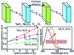
Alternate layered nanostructures are synthesized with thiol-modified niobate nanosheets or tantalate nanosheets and alkene-modified tungstate nanosheets via a thiol–ene click reaction. The stacking distance of the nanosheets is increased linearly with the increase of the carbon number contained in the bridging chain, and controlled within the nanometer order by changing the carbon number generated by the thiol–ene click reaction. Different behaviors observed in the absorption spectra of the two combinations are discussed in terms of the electronic interaction between the neighboring nanosheets. The absorption peak attributed to the bandgap transition of tungstate in the absorption spectrum of the alternate layered nanostructure of niobate and tungstate is blue-shifted with the decrease of the stacking distance. This observation leads us to conclude that the density of states of the tungstate nanosheets is changed by formation of a p–n junction in the alternate layered structure. On the other hand, when the stacking distance of the alternate layered nanostructure of tantalate and tungstate is varied, there are no shifts of the absorption peak attributed to the bandgap transition of tungstate. This result indicates that the electronic structure of the tantalate nanosheets and the tungstate nanosheets in the alternate layered structure are independent. It is discovered that the electronic structures of the alternate stacking structures constructed by thiol–ene click reaction can be modified by changing the stacking distance of the alternate layered nanostructures, controlled by changing the carbon number.


Introduction

Metal oxide nanosheets obtained by exfoliation of layered metal oxides have two-dimensional anisotropy because the thickness and the lateral size of the nanosheets are ca. 1 nm and over 100 nm, respectively.1–3 Generally, these nanosheets are single crystal, and possess an enormous specific surface area. Therefore, when the nanosheets are used as catalysts or electrodes, the chemical reactions performed therein are enhanced compared to bulk materials.4–8

There are many reports of designing the fine structures with very large heterojunction interface by alternately stacking of two different nanosheets. General approaches to construct the alternate layered nanostructure of nanosheets are the following two ways; (1) alternately impregnating a substrate into two types of nanosheets dispersion,9–11 and (2) self-assembled stacking of dispersed anionic nanosheets and cationic nanosheets in one-pot.12,13 At the interface formed by alternately stacking, electrons are effectively transferred from one to the other.12–15 Moreover, ferroelectricity led by formation of singular polarized state at the interface was observed.16 However, it is impossible to systematically control a stacking distance of nanosheets in nanometer order for the alternate layered structure constructed by these methods in which two different nanosheets are aggregated by Coulomb attraction or van der Waals' forces. In addition, when the alternate layered structure constructed by these methods are used as catalysts, the interface of the nanosheets hardly plays a role of reaction field because it is difficult for the substrates to diffuse into the space between the nanosheets which are conjugated very closely each other.

Recently, our group reported a novel synthesis method for constructing alternate layered nanostructure of thiol modified titanate nanosheets and alkene modified tungstate nanosheets via thiol–ene click reaction.17 The stacking distance of the alternate layered nanostructure can be controlled within sub-nanometer order by changing a carbon chain length of the bridging chain generated by thiol–ene click reaction. Moreover, when the nanostructure was irradiated with ultraviolet light, both the titanate and the tungstate were photoexcited, and then the electrons in the conduction band of titanate were transferred to the conduction band of tungstate. Finally the nanostructure turns to a charge separation state where electrons are stored in the conduction band of tungstate. The mechanism of the photoinduced electron transfer was understood using the through-space model. The photoinduced electron transfer can be controlled by changing the distance of the electron transfer which is determined according to the stacking distance of the nanosheets herein.

Cationic species can be intercalated into the interlayer space of the alternate layered nanostructure generated by thiol–ene click reaction. Then the intercalated molecules or cations can experience the large interface area between the nanosheets provided as the reaction space. Therefore, electron transfer between the intercalated molecules and the nanosheets should effectively proceed. In fact, when the alternate layered nanostructure with intercalated methylene blue between the nanosheets was irradiated with UV light, methylene blue was decomposed effectively through oxidation by the holes accumulated in the valence band in titanate.18 On the other hand, by intercalation of rhodamine B into the alternate layered nanostructure, electrons stored in the conduction band of the tungstate were effectively transferred to the vacant HOMO level of the excited rhodamine B under visible light irradiation.19

The main purpose of this work is to engineer the hetero interface of two semiconductor nanosheets in the alternate layered nanostructure by the following two ways. The first one is to synthesize some combinations of the different semiconductor nanosheets, by which we can change the relative relations of the band structures for the alternate layered nanostructures consisting of different combinations of semiconductor nanosheets. The proper change of the relative band positions between the combined two semiconductors would lead to an efficient photoinduced charge separation or a novel photofunction. We synthesized the alternate layered structure for the combinations of niobate–tungstate and tantalate–tungstate. The other one is to change the stacking distance between the two different nanosheets in the alternate layered nanostructure. To change the stacking distance, the carbon number contained in the bridging chain generated by thiol–ene click reaction was varied as 6, 11, 14 and 19. The synthetic strategy of the alternate layered nanostructure is shown in Scheme 1. The starting materials were layered metal oxides. At first, the interlayer space between the nanosheets constituting each metal oxide was made hydrophobic by inserting n-octylamine (step (a)). Secondly, after the inner lateral surface of each nanosheet being modified with thiol group or alkene group using silane coupling reagent (step (b)), the layered materials were exfoliated into nanosheets in N,N-dimethylformamide by ultrasonication (step (c)). The dispersions of two different semiconductor nanosheets were mixed, and then azobisisobutyronitrile (AIBN) was introduced into the reaction mixture (step (d)), finally resulting in the alternate layered nanostructure consisting of two different semiconductor nanosheets. The stacking distances of the alternate layered nanostructures of niobate–tungstate and tantalate–tungstate were determined by XRD in comparison with that of titanate–tungstate. The electronic structures of these alternate stacking structures were investigated using the diffuse reflectance spectroscopy. Moreover, the tilt angle of the bridging chains in the interlayer space was discussed on the basis of the structures of the lateral surface of each semiconductor nanosheet, such as the density of hydroxyl groups.


image file: c6ra13785g-s1.tif
Scheme 1 Synthetic strategy of the alternate layered nanostructure.

Experimental

Materials

All reactants and solvents were used as supplied. KNO3, Nb2O5, Ta2O5, Bi2O3, hydrochloric acid, nitric acid, acetone, toluene, n-octylamine, heptane, ethanol, N,N-dimethylformamide (DMF) and azobisisobutyronitrile (AIBN) were purchased from Wako Pure Chemical Industries, Ltd. Rb2CO3 was purchased from Sigma-Aldrich, Inc. WO3 (99.99%) was purchased from High Purity Materials KOJUNDO CHEMICAL LABORATORY Co., Ltd. 3-Mercaptopropyltrimethoxysilane and allyltrimethoxysilane were purchased from Tokyo Kasei Co. Ltd, Japan. 7-Octenyltrimethoxysilane and 11-mercaptoundecyltrimethoxysilane were purchased from Gelest Inc. Water was purified by a Millipore Direct-Q 3 Ultrapure Water System to a resistivity of 18.2 MΩ cm.

Synthesis of thiol group-modified niobate nanosheet

HNb3O8 was obtained using the reported procedure.20,21 Nb2O5 (9.86 g) and KNO3 (2.50 g) in the stoichiometric ratio of HNb3O8 were mixed by a pestle and mortar. The powder was put in a platinum crucible and calcined at 900 °C for 20 h. Then, KNb3O8 was obtained. KNb3O8 (3.00 g) suspended in 2 M nitric acid (300 mL) was heated at 80 °C for 1 h under microwave irradiation with Microsynth (Milestone Inc.). The reaction product was centrifuged and dried at 40 °C under vacuum overnight, and then HNb3O8 was obtained. The product was analyzed by XRD, ensuring the pure product without any impurity. HNb3O8 (1.00 g) was dispersed in a mixture of n-octylamine (6.9 mL) and heptane (13.8 mL). After stirred for 6 h at 60 °C, the reaction mixture was centrifuged and dried under vacuum overnight. n-Octylamine was intercalated into HNb3O8 as n-octylammonium through protonation by the interlayer proton. Then, n-octylammonium intercalated layered niobate, C8N–Nb3O8, was obtained. As a result of the intercalation of n-octylammonium, the interlayer distances between the two nanosheets of niobate were expanded. C8N–Nb3O8 (0.40 g) was dispersed in toluene (40 mL), and then bubbled with nitrogen for 30 min. 3-Mercaptopropyltrimethoxysilane (0.2 mL) or 11-mercaptoundecyltrimethoxysilane (0.32 mL) was introduced into the reaction mixture under nitrogen. After stirred for 48 h at 90 °C, the reaction mixture was centrifuged and washed with ethanol, and then layered niobate modified with thiol group, C8N–Nb3O8–CnSH (n = 3, 11) was obtained. C8N–Nb3O8–CnSH (0.10 g) was ultrasonicated in N,N-dimethylformamide (200 mL) for 60 min and exfoliated into the nanosheets. The dispersion was centrifuged at 4000 rpm for 10 min to remove layered materials which were not exfoliated.

Synthesis of thiol group modified tantalate nanosheet

HTaO3 was obtained using the reported procedure.22 Ta2O5 (1.88 g) and Rb2CO3 (1.00 g) in the stoichiometric ratio of HTaO3 were mixed by a pestle and mortar. The powder was put into a platinum crucible and calcined at 900 °C for 20 h. Then, RbTaO3 was obtained. RbTaO3 (1.00 g) suspended in 1 M hydrochloric acid (100 mL) was heated at 80 °C for 1 h under microwave irradiation by Microsynth. The reaction product was centrifuged and dried under vacuum overnight, and then HTaO3 obtained. The product was analyzed by XRD, ensuring the pure product without any impurity. HTaO3 (0.50 g) was dispersed in a mixture of n-octylamine (5.0 mL) and heptane (10 mL). After stirred for 4 h at room temperature, the reaction mixture was centrifuged and dried under vacuum overnight. n-Octylamine was intercalated into HTaO3 as n-octylammonium in protonation with the interlayer proton. Then, n-octylammonium intercalated layered tantalate, C8N–TaO3, was obtained. As a result of the intercalation of n-octylammonium, the interlayer distances between the nanosheets of tantalate were expanded. C8N–TaO3 (0.50 g) was dispersed in toluene (50 mL), and then bubbled with nitrogen for 30 min. 3-Mercaptopropyltrimethoxysilane (0.50 mL) or 11-mercaptoundecyltrimethoxysilane (1.0 mL) was introduced into the reaction mixture under nitrogen. After stirred for 48 h at 90 °C, the reaction mixture was centrifuged and washed with ethanol, and then layered tantalate modified with thiol group, C8N–TaO3–CmSH (m = 3, 11) was obtained. C8N–TaO3–CmSH (0.1 mg) was ultrasonicated in N,N-dimethylformamide (200 mL) for 60 min and exfoliated into the nanosheets. The dispersion was centrifuged at 4000 rpm for 10 min to remove layered materials which were not exfoliated.

Synthesis of alkene group-modified tungstate nanosheet

Alkene modified tungstate nanosheet was obtained using the reported procedure.17 WO3 (3.00 g) and Bi2O3 (3.02 g) in the stoichiometric ratio of Bi2W2O9 were mixed by a pestle and mortar. The powder was put in a platinum crucible and calcined at 800 °C for 48 h. Then, Bi2W2O9 was obtained. Bi2W2O9 (5.00 g) suspended in 6 M hydrochloric acid (1 L) was heated at 80 °C for 1 h under microwave irradiation by Microsynth. The reaction product was centrifuged and dried under vacuum overnight, and then H2W2O7 was obtained. The product was analyzed by XRD, ensuring the pure product without any impurity. H2W2O7 (1.0 g) was dispersed in a mixture of n-octylamine (10 mL) and heptane (20 mL). After stirred for 4 h at room temperature, the reaction mixture was centrifuged and dried under vacuum overnight. n-Octylamine was intercalated into H2W2O7 as n-octylammonium through protonation with the interlayer proton. Then, the n-octylammonium intercalated layered tungstate, C8N–W2O7, was obtained. As a result of the intercalation of n-octylammonium, the interlayer distances between the nanosheets of tungstate were expanded. C8N–W2O7 (0.50 g) was dispersed in toluene (50 mL), and then bubbled with nitrogen for 30 min. Allyltrimethoxysilane (1.0 mL) or 7-octenyltrimethoxysilane (1.5 mL) was introduced into the reaction mixture under nitrogen. After stirred for 48 h at 90 °C, the reaction mixture was centrifuged and washed with ethanol, and then layered tungstate modified with alkene group, C8N–W2O7–Ckene (k = 3, 8) was obtained. C8N–W2O7–Ckene (0.10 mg) was ultrasonicated in N,N-dimethylformamide (200 mL) for 60 min and exfoliated into the nanosheets. The dispersion was centrifuged at 4000 rpm for 10 min to remove layered materials which were not exfoliated.

Click-reaction of organic modified nanosheets

The dispersions of thiol group-modified niobate nanosheets or tantalate nanosheets were mixed with the dispersions of alkene group-modified tungstate nanosheets. The mixing ratio in the weights of the nanosheets was 7[thin space (1/6-em)]:[thin space (1/6-em)]6 (niobate/tungstate) or 7[thin space (1/6-em)]:[thin space (1/6-em)]5 (tantalate/tungstate) which was estimated as that having the areas of the lateral surface of each sheet to be equal. The mixture was bubbled with nitrogen for 30 min, and then AIBN of the amount of half of the equivalent to the thiol groups was injected into the reaction mixture under nitrogen. After stirred for 24 h at 80 °C, the reaction mixture was centrifuged for 10 min at 6000 rpm, and then washed with ethanol. The resultant sample was dried under vacuum overnight. Then the alternate layered nanostructure was obtained.

Characterization

X-ray diffraction (XRD) analyses were carried out using a Philips X'Pert MPD-OEC diffractometer with bent crystal monochromated CuKα radiation. Elemental analysis was carried out with YANACO CHN corder MT-6 and Leeman Labs, INC U.S.A Prodigy ICP (ICP-OES). For ICP-OES, the powder samples were dissolved in hydrofluoric acid. The morphology of nanosheets was observed by Nanocute (AFM), SII NanoTechnology Inc. The sample was fabricated by dipping a Si wafer into the nanosheet dispersion. Transmission electron microscopy (TEM) images were collected by a JEOL JEM-2010 instrument operated at 200 keV. Dispersion containing the samples was dropped on a carbon-coated Cu grid TEM sample holder. Scanning electron microscopy (SEM) images were collected by a Hitachi S-5500 scanning electron microscope equipped with an energy dispersive X-ray spectroscope (EDS). UV-Vis diffuse reflectance spectra were recorded on a JASCO V-570 equipped with a diffused reflex unit, ISN-470.

Results and discussion

Thiol- or alkene-modified nanosheets

Fig. 1(a) shows the XRD patterns of thiol-modified layered niobate and its precursors. All the peaks of layered potassium niobate, KNb3O8, as the starting material and layered niobate, HNb3O8, were indexed according to the literatures, showing that these compounds were synthesized properly and contained no impurity.20,21,23 The orientation of the layered structure is [010], and the unit cell includes the two layers of niobate. Therefore, the d value of the (020) peak is corresponding to the distance of neighboring layers. The d value of the (020) peak was determined as 1.13 nm for the center-to-center distance of the layers. While the thicknesses of the niobate is calculated as 0.70 nm from the crystal structure, the large distance of the neighboring layers in HNb3O8 can be explained by expansion of the interlayer space by swelling with the hydration water. After the generation of C8N–Nb3O8 through the reaction of HNb3O8 with n-octylamine, a (001) peak appeared at 2theta = 3.70°, indicating the expansion of the layered structure resulting in the d value (2.39 nm) of the (001) peak for the center-to-center distance of the layers. The interlayer distance was expanded through the intercalation of n-octylamine by 1.26 nm herein. When C8N–Nb3O8 was reacted with 3-mercaptopropyltrimethoxysilane or 11-mercaptoundecyltrimethoxysilane, the d values of the (001) peak were increased through the reaction to d = 2.45 nm and 2.43 nm, respectively. This result indicated that the interlayer distance was expanded through the reactions of these silane coupling reagents on the lateral surface of the nanosheets between the interlayer spaces. The diffraction peaks at 2theta = 16.1°, 22.2°, 25.9°, 28.0°, 29.2°, 32.0°, 38.2°, 43.7°, 45.9°, 48.0°, and 51.8° were not shifted through the reaction with silane coupling reagents. This result means that these diffraction peaks were not related to the expansion of the interlayer distance. Therefore, these diffraction peaks can be attributed to the diffraction planes which were independent of the layered structure orientation.
image file: c6ra13785g-f1.tif
Fig. 1 (a) XRD patterns of thiol-modified layered niobate and the precursors. (b) AFM image of niobate nanosheets. (c) Cross-sectional profile on the dotted line described in (b). (d) Histogram of the height of niobate nanosheets measured by AFM.

To confirm the intercalation of n-octylammonium and silane coupling reagent in a quantitative way, ICP-OES and CHN elemental analysis were carried out (Table 1). The amounts of the introduced n-octylammonium and silane coupling reagent were estimated by the weight fraction of nitrogen and silicon, respectively. Dividing the estimated amounts of these introduced molecules by the area of the lateral surface of the niobate layers calculated from the crystal structure of layered niobate, the amounts of the molecules per unit areas were estimated as 5.8 molecules per nm2 for n-octylammonium and 0.99 molecules per nm2 for 3-mercaptopropyltrimethoxysilane, respectively. The density of hydroxyl groups on the lateral surface of the niobate layer was calculated as 8 nm−2 from the crystal structure of layered niobate.24 Therefore, all intercalated n-octylammonium species can be coordinated to the hydroxyl groups on the lateral surface of the nanosheets in the monodentate mode, and all 3-mercaptopropyltrimthoxysilane molecules can be immobilized to the hydroxyl groups in the monodentate or bidentate mode.

Table 1 Elemental ratio of modified layered metal oxidesa
  Cb (wt%) Hb (wt%) Nb (wt%) Nbc (wt%) Tac (wt%) Wc (wt%) Sic (wt%) Od (wt%) Se (wt%) Amount (wt%) n-Octylammoniumf (molecules per nm2) Silane coupling reagentf (molecules per nm2)
a n.t. = not tested.b Determined by CHN elemental analysis.c Determined by ICP-OES.d Estimated by wt% of metal using composition formula, MOx.e Estimated by wt% of Si as equal mole amount of Si and S, since Si and S derive from silane coupling reagent.f Estimated by crystal structure and wt% of N or Si.
C8N–Nb3O8 14.7 3.2 2.1 n.t.  
C8N–Nb3O8–C3SH 14.2 3.2 1.9 52.4 0.65 24.1 0.74 97.16 5.8 0.99
C8N–Nb3O8–C11SH 15.3 3.2 1.9 n.t. n.t.    
C8N–TaO3 14.4 3.4 2.1 n.t.  
C8N–TaO3–C3SH 10.7 2.4 1.2 63.8 1.3 16.9 1.5 97.77 0.60 0.32
C8N–TaO3–C11SH 15.1 3.2 1.3 n.t. n.t.    
C8N–W2O7 21.7 4.3 3.2 n.t.  
C8N–W2O7–C3ene 19.1 3.9 2.7 54.8 0.82 16.7 0.9 98.97 4.4 0.66
C8N–W2O7–C8ene 19.5 3.9 2.7 n.t. n.t.    


Fig. 1(b) and (c) show an AFM image of the 3-mercaptopropyltrimethoxysilane-modified niobate nanosheets, and the cross-sectional profile along the line drawn in Fig. 1(b), respectively. The profile indicates a trapezium shape with a height of ca. 1.1 nm, probably corresponding to a tantalate nanosheet. The distribution of the thicknesses of the nanosheets measured in the AFM images is shown as a histogram in Fig. 1(d), which exhibits a relatively symmetrical distribution with the maximum at 0.9–1.2 nm, and the local maximum value was indicated at 1.5–1.8 nm. The thickness of the niobate nanosheets was calculated to be 0.7 nm from the crystal structure of niobate.24 Therefore, the sheets with the thickness of 0.9–1.2 nm were considered to be a single exfoliated nanosheet, because the lateral surface of the nanosheets was modified with n-octylammonium and thiol group, causing the measured thickness of the modified niobate nanosheets thicker by 0.2–0.5 nm than their crystal structure. The sheets with the thickness of 1.5–1.8 nm were considered to be an aggregation of two exfoliated nanosheets. These results ensured the niobate nanosheets exfoliated into a single layer or double layer.

Fig. 2(a) shows the XRD patterns of thiol modified layered tantalate and its precursors. All the peaks of layered rubidium tantalate, RbTaO3, as the starting material and layered tantalate, HTaO3, were indexed according to the literature.22 The (001) peak of HTaO3 derived from layered structure was employed for determining the d value as 0.72 nm corresponding to the center-to-center distance of the layers. When HTaO3 was reacted with n-octylamine, the d value of the (001) peak was increased to d = 2.86 nm, indicating the expansion of the interlayer gap accompanied by the generation of C8N–TaO3 through the reaction with n-octylamine.


image file: c6ra13785g-f2.tif
Fig. 2 (a) XRD patterns of thiol modified layered tantalate and the precursors. (b) AFM image of tantalate nanosheets. (c) Cross-sectional profile on the dotted line described in (b). (d) Histogram of the height of tantalate nanosheets measured by AFM.

On contrary to the case of niobate described above, the d value of the (001) peak was decreased through the reaction of C8N–TaO3 with 3-mercaptopropyltrimethoxysilane to 2.33 nm. This decrease in the d value induced by the reaction can be understood as the exclusion of n-octylammonium from the interlayer space accompanied by the reaction with 3-mercaptopropyltrimethoxysilane. This exclusion of n-octylammonium was confirmed by CHN elemental analysis shown on Table 1. When the analytical data are compared between C8N–TaO3 and C8N–TaO3–C3SH, the weight fraction of nitrogen was decreased from 2.1 wt% to 1.2 wt% through the reaction of C8N–TaO3 with 3-mercaptopropyltrimethoxysilane, while from 2.1 wt% (C8N–Nb3O8) to 1.9 wt% (C8N–Nb3O8–C3SH). Therefore, compared to the layered niobate, much n-octylammonium ions were excluded from the layered tantalate. The different tendency of the exclusion can be explained by the density of hydroxyl group. The density of hydroxyl group of niobate and tantalate can be estimated as 8.0/nm2 and 2.45/nm2 from crystal structure, respectively, so that the intercalated n-octylammonium in niobate is more likely to be kept in the interlayer space than that in tantalate. On the other hand, the reaction of C8N–TaO3 with 11-mercaptoundecyltrimethoxysilane induced the increase in the d value of the (001) peak to d = 3.23 nm. The introduction of 11-mercaptoundecyltrimethoxysilane should expand the interlayer distance in spite of the exclusion of n-octylammonium shown as the decrease of the weight percent of N on Table 1. The result observed for tantalate might be a result of the trade-off between the shrinkage by the exclusion of ammonium species and the expansion by introducing the long carbon chain. The diffraction peaks at 2theta = 28.1°, 37.9° and 43.0° were not shifted through the reaction with silane coupling reagents. Therefore, these diffraction peaks can be attributed to the diffraction planes which were independent of the layered structure orientation.

The amounts of the introduced n-octylammonium and silane coupling reagent were estimated by the weight fractions of nitrogen and silicon. Dividing the estimated amounts of these introduced molecules by the area of the lateral surface of the layers of tantalate calculated from the crystal structure of layered tantalate, the amounts of the molecules per unit areas were estimated as 0.60 molecules per nm2 for n-octylammonium and 0.32 molecules per nm2 for 3-mercaptopropyltrimethoxysilane, respectively. The density of hydroxyl groups on the lateral surface was calculated to 2.45 nm−2 from the crystal structure of layered tantalate.25 Therefore, all the intercalated n-octylammonium species can be coordinated to hydroxyl groups on the surface of the nanosheets in the monodentate mode, and all of the 3-mercaptopropyltrimthoxysilane molecules can be immobilized by the reaction with hydroxyl groups in the monodentate or bidentate mode.

Fig. 2(b) and (c) show an AFM image of the 3-mercaptopropyltrimethoxysilane-modified tantalate nanosheets, and the cross-sectional profile along the line drawn in Fig. 2(b), respectively. The profile indicates a trapezium shape with a height of ca. 1.5 nm, probably corresponding to a tantalate nanosheet. The distribution of the thicknesses of the nanosheets measured in the AFM images is shown as a histogram in Fig. 2(d), which exhibits a relatively symmetrical distribution with the maximum at 1.2–1.8 nm. The thickness of the tantalate nanosheets was calculated to be 0.8 nm from the crystal structure of tantalate.25 Therefore, the sheets with the thickness of 1.2–1.8 nm were considered to be a single exfoliated nanosheet, because the lateral surface of the nanosheets was modified with n-octylammonium and thiol group, causing the measured thickness of the modified tantalate nanosheets thicker by 0.4–1.0 nm than their crystal structure. The sheets with the thickness over 3.0 nm were considered to be an aggregation of two or more exfoliated nanosheets. These results ensured the tantalate nanosheets exfoliated into a single layer or double layer.

Fig. S1 shows the XRD patterns of alkene-modified layered tungstate and its precursors. The XRD pattern of layered tungstate reacted with n-octylammonium was in good agreement with the reported one for n-octylammonium intercalated layered tungstate.17 The (001) peak of C8N–W2O7 was derived from layered structure, by which the d value of the (001) peak was determined as 2.56 nm for the center-to-center distance of the layers. The d value of the (001) peak was decreased through the reaction of C8N–W2O7 with allyltrimethoxysilane to d = 2.29 nm. This result can be understood as due to exclusion of n-octylammonium from the interlayer space in the same manner as tantalate, which was induced by the intercalation of 3-mercaptopropyltrimethoxysilane. This explanation is supported by the decrease in the amount of nitrogen for C8N–W2O7–C3ene and C8N–W2O7–C8ene compared to C8N–W2O7. On the other hand, the reaction of C8N–W2O7 with 7-octenyltrimethoxysilane led to increasing of the d value of the (001) peak to d = 2.59 nm. The result observed for tungstate might also be a result of the trade-off between the shrinkage by the exclusion of ammonium species and the expansion by the long chain introduced into the interspace as observed for tantalate. The diffraction peaks at 2theta = 24.5°, 34.1°, 50.0° and 55.9° were not shifted through the reaction with silane coupling reagents. Therefore, these diffraction peaks can be attributed to the diffraction planes which were independent of the layered structure orientation. Fig. S2(a) and (b) show an AFM image of the allyltrimethoxysilane-modified tungstate nanosheets, and the cross-sectional profile along the line drawn in Fig. S2(a), respectively. The profile indicates a trapezium shape with a height of ca. 1.8 nm, probably corresponding to a tungstate nanosheet.

The amounts of the introduced n-octylammonium and silane coupling reagent were estimated by the weight fractions of nitrogen and silicon (Table 1). Dividing the estimated amounts of these introduced molecules by the area of the lateral surface of the layers of tungstate calculated from the crystal structure, the amounts of the molecules per unit areas were estimated as 4.4 molecules per nm2 for n-octylammonium and 0.66 molecules per nm2 for 3-mercaptopropyltrimethoxysilane, respectively. The density of the interlayer hydroxyl groups of tungstate was calculated as 6.8 nm−2 from the crystal structure of layered tungstate.26 Therefore, all the intercalated n-octylammonium can be coordinated to hydroxyl groups on the lateral surface of the nanosheets in the monodentate mode, and all the 3-mercaptopropyltrimthoxysilane molecules can be immobilized to hydroxyl groups in the monodentate or bidentate mode.

Alternate layered nanostructure of niobate and tungstate nanosheets

Fig. 3(a) shows XRD patterns of the alternate layered nanostructure of niobate and tungstate nanosheets synthesized by thiol–ene click reaction, in which Cn+k Nb3O8–W2O7 denotes the alternate layered structure consisting of Nb3O8–CnSH (n = 3 or 11) and W2O7–Ckene (k = 3 or 8), and the carbon number in the bridging chain generated by thiol–ene click reaction is n + k. These XRD spectra demonstrated the appearance of the peaks at 2theta = 5.98–6.92°, demonstrating the formation of a new layered structure: 2theta = 6.92° (d = 1.28 nm) for C6 Nb3O8–W2O7, 6.46° (d = 1.37 nm) for C11 Nb3O8–W2O7, 6.14° (d = 1.38 nm) for C14 Nb3O8–W2O7, and 5.98° (d = 1.48 nm) for C19 Nb3O8–W2O7. Since these d values were increased with the number of carbon atoms, these peaks were attributed to an alternately repeated structure of niobate nanosheets and tungstate nanosheets. These peaks were attributed to second-order diffraction of the alternate layered structure since the first-order diffraction attributed to the neighbouring nanosheets of niobate and niobate, or tungstate and tungstate is cancelled in the XRD patterns due to antiphase of the diffraction of the niobate against the diffraction of the tungstate. The diffraction plane present at both lateral planes of tungstate and niobate in the alternate structure is repeated as the plane with the high electronic density. Then the d value should correspond to the centre-to-centre distance of the neighbouring nanosheets of niobate and tungstate. Therefore, we can index these peaks as (002) plane. In C6 Nb3O8–W2O7, the interlayer distance between the edge of the niobate nanosheet and that of the tungstate nanosheet was estimated as 0.43 nm because the thicknesses of the niobate and the tungstate nanosheet were calculated as 0.70 nm and 1.01 nm using the crystal structures of these, respectively. Similarly, the interlayer distances of the C11 Nb3O8–W2O7, C14 Nb3O8–W2O7 and C19 Nb3O8–W2O7 were estimated as 0.52 nm, 0.53 nm and 0.63 nm, respectively.
image file: c6ra13785g-f3.tif
Fig. 3 (a) XRD patterns of alternate layered nanostructures of niobate and tungstate. (□) Attributed to in-plane diffraction of tungstate nanosheets, (△) attributed to in-plane diffraction of niobate nanosheets. (b) SEM image of the alternate layered nanostructure of niobate and tungstate. (c) TEM image of the alternate layered nanostructure of niobate and tungstate. (d) Diffuse reflectance spectra of alternate layered nanostructure of niobate and tungstate (red: C6 Nb3O8–W2O7, orange: C11 Nb3O8–W2O7, green: C14 Nb3O8–W2O7, blue: C19 Nb3O8–W2O7, broken gray line: alkene-modified layered tungstate, broken black line: thiol-modified layered niobate.) (e) Results obtained by the deconvolution of the diffuse reflectance spectra.

A peak indexed with an asterisk (*) observed at 2theta = 3.31° for the XRD patterns should be due to the unreacted layered tungstate and unreacted layered niobate since the d value was same as the (001) plane observed for unreacted alkene modified layered tungstate and thiol-modified layered niobate. We can exclude a possibility of the formation of the layered structure of sole niobate nanosheets because of the thiol–ene click chemistry employed for constructing the alternate stacked structure. The mixture ratio of the alternate layered structure and the precursors was roughly estimated to be approximately 60[thin space (1/6-em)]:[thin space (1/6-em)]40 in all samples by the peak intensity from the XRD patterns on the assumption of the small difference in the diffraction intensities of the (002) plane of alternate layered nanostructure and the (001) plane of the precursors. The peaks indexed with triangles (2theta = 25.9°, 32.0°, 38.2°, 48.0° and 51.8°) or squares (2theta = 24.5°, 34.1°, 50.0° and 55.9°) were attributed to the in-plane diffraction for the niobate or tungstate nanosheets, respectively, which were independent of the layered structure orientation. Therefore, the crystal structures of the nanosheets were maintained even after the nanosheets were assembled in the alternate layered nanostructure.

Fig. 3(b) shows a SEM image of C6 Nb3O8–W2O7, showing the particle size of C6 Nb3O8–W2O7 as ca. 10 μm. Fig. S3 shows an EDX mapping of Nb and W on the SEM image, showing the uniform distribution of these elements over the whole area. This uniformity strongly supported the homogeneous formation of the stacking structure of the niobate nanosheets and the tungstate nanosheets. The average ratio of Nb/W was determined as 2.6 by EDX analysis in the whole area of the TEM image. This ratio was in a little excess of Nb compared to the mixture ratio of Nb/W = 2.3 used for the synthesis of the alternate layered structure. A TEM image of the alternate layered nanostructure is shown in Fig. 3(c). Fig. S4(a) shows an EDX spectrum corresponding to the TEM image. Since the peaks are attributed to Nb, W, S and Si, the stripe patterns observed in the TEM image should be attributed to the alternately piled-structure of niobate and tungstate.

Fig. 3(d) shows diffuse reflectance spectra of the alternate layered nanostructures of niobate and tungstate in addition to those of thiol-modified layered niobate and alkene-modified layered tungstate. The reflectance spectra of the alternate layered nanostructure of niobate and tungstate appeared like the simple overlaps of each component of the niobate nanosheets and the tungstate nanosheets, in which the absorption peak was fixed for the niobate nanosheet but that was shifted for the tungstate nanosheet depending on the length of the bridging chains. The absorption of tungstate was shifted to the shorter wavelength for the alternate layered nanostructure with the shorter carbon chain. Furthermore, the absorption edges of all the alternate layered structures were observed at λ = 470 nm as approximately same as that of layered tungstate.

The absorption spectra were deconvoluted as shown in Fig. S5, in which the absorption peak of niobate was fixed at the wavelength observed in each reflectance spectrum and that of tungstate was changed for obtaining the properly simulated shapes of the whole spectra. Gaussian distribution was assumed for each simulated spectrum. The peak wavelengths and the peak areas obtained in the simulation are summarized in Fig. 3(e). Beside the peaks at 260–263 nm (Peak 1) attributed to the bandgap absorption of niobate, the peaks at 277–319 nm (Peak 2) attributed to the bandgap transition of tungstate nanosheet shifted to shorter wavelength for the alternate layered nanostructures with the shorter bridging chains as summarized below.

C6 Nb3O8–W2O7 (277 nm) < C11 Nb3O8–W2O7 (284 nm) < C14 Nb3O8–W2O7 (296 nm) < C19 Nb3O8–W2O7 (319 nm) < layered tungstate (361 nm)

The absorption of tungstate shifts back to that of the layered tungstate when the stacking distance becomes large, namely red-shift. This means that the band gap gets close to that of sole tungstate when the interaction between tungstate and niobate gets weak. Since the bandgap energy of the layered tungstate is lower than that of tungstate alternately stacked with niobate, the interaction between the tungstate and niobate should broaden the bandgap energy of tungstate.

It should be pointed out here that the contents of the tungstate nanosheets in all the samples are nearly the same. Then we have been led to a conclusion that the electronic structure of the tungstate nanosheet is modified in the alternate layered structures depending on the stacking distance. The p–n junction might be formed at the interface of niobate and tungstate nanosheets in the alternate layered nanostructure, possibly changing the electronic structure of the tungstate nanosheet depending on the stacking distance. The area of the interface between the tungstate and niobate nanosheets is extraordinarily large, inducing the modification of the electronic structure which cannot be observed in the conventional nanohybrid systems. We would point out that the similar change in the absorption spectra of the tungstate nanosheet was also observed for the alternate layered nanostructure of the titanate nanosheets and the tungstate nanosheets (Fig. S6). It is assumed as a possible reason of the spectral change observed here that the electrons could be transferred from niobate to tungstate in the alternate stacked structure because of the difference of the Fermi levels between niobate and tungstate. Further investigations are in progress for observing the electron transfer between the two nanosheets.

Alternate layered nanostructure of tantalate and tungstate nanosheets

Fig. 4(a) shows XRD patterns of the alternate layered nanostructure of the tantalate nanosheets and the tungstate nanosheets. Here, Cn+k TaO3–W2O7 denotes the alternate layered structure of tantalate and tungstate synthesized by thiol–ene click reaction of TaO3–CmSH (n = 3 or 11) and W2O7–Ckene (k = 3 or 8), in which the carbon number contained in the bridging chain is n + k. The XRD spectra demonstrate appearance of the peaks at 2theta = 3.47–4.31°, showing the formation of a new layered structure: 2theta = 4.31° (d = 2.05 nm) for C6 TaO8–W2O7, 3.84° (d = 2.30 nm) for C14 TaO3–W2O7, and 3.47° (d = 2.55 nm) for C19 TaO3–W2O7. These peaks were attributed to an alternately repeated structure of tantalate nanosheets and tungstate nanosheets. On the basis of the same discussion described in the alternate layered structure of niobate and tungstate, we can index these peaks as (002) plane. Therefore, in C6 TaO3–W2O7, the interlayer distance of the tantalate nanosheets and the tungstate nanosheets was estimated as 1.14 nm because the thicknesses of the tantalate and the tungstate nanosheets were calculated as 0.81 nm and 1.01 nm, respectively. Similarly, the interlayer distances of the C14 TaO3–W2O7 and C19 TaO3–W2O7 were estimated as 1.39 nm and 1.64 nm, respectively.
image file: c6ra13785g-f4.tif
Fig. 4 (a) XRD patterns of alternate layered nanostructures of tantalate and tungstate. (□) Attributed to in-plane diffraction of tungstate nanosheets, (△) attributed to in-plane diffraction of tantalate nanosheets. (b) SEM image of the alternate layered nanostructure of tantalate and tungstate. (c) TEM image of the alternate layered nanostructure of tantalate and tungstate. (d) Diffuse reflectance spectra of alternate layered nanostructure of tantalate and tungstate. Red: C6 TaO3–W2O7, green: C14 TaO3–W2O7, blue: C19 TaO3–W2O7, broken gray line: alkene-modified layered tungstate, broken black line: thiol-modified layered tantalate. (e) Results obtained by the deconvolution of the diffuse reflectance spectra.

A peak indexed with an asterisk (*) showed the presence of unreacted layered tungstate and layered tantalate since the d value was same as the (001) plane observed for alkene-modified layered tungstate and thiol-modified layered tantalate. Then we should mention here that the obtained sample is not pure alternate layered structure of tantalate nanosheets and tungstate nanosheets, containing unreacted residual layered tungstate and layered tantalate. The peaks indexed with triangles (2theta = 28.1° and 37.9°) or squares (2theta = 24.5°, 34.1°, 50.0° and 55.9°) were attributed to the diffraction planes for tantalate or tungstate, respectively, which were independent of the layered structure orientation. Therefore, the crystal structures of the nanosheets were maintained even after the nanosheets were assembled in the alternate layered nanostructure.

Fig. 4(b) shows a SEM image of C6 TaO3–W2O7. The particle size of C6 TaO3–W2O7 was ca. 10 μm. Fig. S7 shows an EDX mapping of Ta and W elements on the SEM image. The mapping showed that Ta and W were distributed uniformly over the whole area. This uniformity strongly supported the homogeneous formation of the stacking structure of the tantalate nanosheets and the tungstate nanosheets. The average element ratio of Ta/W was determined as 1.35 by the EDX analysis, being in good agreement with the mixture ratio employed in the synthesis of the alternate layered structure as Ta/W = 1.39. The TEM image of the alternate layered nanostructure is shown in Fig. 4(c). Since the peaks of EDX spectrum on the TEM image shown in Fig. S4(b) are attributed to Ta, W, S and Si, the stripe patterns observed in the TEM image should be attributed to the alternately piled structure of tantalate and tungstate.

Fig. 4(d) shows diffuse reflectance spectra of the alternate layered nanostructures of tantalate and tungstate in addition to thiol-modified layered tantalate and alkene-modified layered tungstate. All the spectra observed for all the samples of Cn+k TaO3–W2O7 appeared to be identical, having the same shapes in the same region of the wavelength, suggesting the same electronic structure for all. The shape of the whole spectrum appeared to be the overlap of the two reflectance spectra of tantalate and tungstate. Then the spectra were deconvoluted into the two components, in which the absorption peak of tantalate was fixed at the wavelength observed for thiol-modified layered tantalate. The absorption peak of alkene-modified layered tungstate was changed in the deconvolution for obtaining the properly simulated shapes of the whole spectra (Fig. S8). Gaussian distribution was assumed for each component spectrum. The peak wavelength and the peak area obtained by the deconvolution are summarized in Fig. 4(e).

The peaks at 257–262 nm (Peak 1) should be attributed to the bandgap transition of the tantalate nanosheet. On the other hand, the peaks at 293–298 nm (Peak 2) were considered to be attributed to the bandgap transition of the tungstate nanosheet. In clear contrast with the blue-shift observed for the reflectance spectra of tungstate component in the alternate layered nanostructure of niobate and tungstate, no shift in the peak was observed with the change of the carbon number contained in the bridging chain. However, the wavelength of the peak attributed to the bandgap transition of tungstate in the alternate layered structure was observed at the shorter wavelength by ca. 80 nm compared to that of sole layered tungstate. This result suggests the presence of the interaction in the electronic structures between tantalate and tungstate in the alternate layered structure as well as in the alternate layered structure of niobate and tungstate, or titanate and tungstate.18 Further investigation is required to understand this.

Relationship between the interlayer distance and the length of the bridging chain

The interlayer distances in the alternate layered nanostructures are plotted against the carbon numbers contained in the bridging chains generated by thiol–ene click reaction for the two combinations of the alternate layered structures, i.e., niobate–tungstate, and tantalate–tungstate (Fig. 5). The data of the alternate layered structure of titanate and tungstate referred from our previous report are plotted herein together.18 The stacking distances of the nanosheets were increased linearly with the increase of the carbon numbers. The approximate straight lines obtained by the least squares method are drawn in Fig. 5 for the three combinations. The slopes of the line correspond to the increments of the stacking distances by adding one carbon to the bridging chains. For example, the increment of the stacking distance of the alternate layered structure of tantalate and tungstate was 0.038 nm by adding one carbon. From the slope of the line, dr/dn, the average tilt angle of the bridging chains in the interlayer space, θ, was calculated using the following eqn (1),
 
image file: c6ra13785g-t1.tif(1)
where it is assumed that the length of the bridging chain is increased by 0.126 nm by adding one carbon to the chain. This increment in the length of the bridging chain was estimated on the basis of the optimized structure of the bridging chain using the Materials studio software from Accelrys Inc. The carbon chain can be considered as a rigid and rectilinear molecule since the interlayer distances were increased linearly with increase in the carbon numbers contained in the bridging chain. The tilt angles estimated here are summarized in Table 2. The tilt angle of the carbon chain in the alternate layered structure of tantalate and tungstate was estimated as 17.6°, while it was 6.9° for that of niobate and tungstate. The tilt angle should be affected by the structure of the lateral surface of each nanosheet, especially by the density of hydroxyl groups. The densities of the hydroxyl groups on the lateral surface of the niobate, titanate and tantalate nanosheets calculated on the basis of their crystal structures were estimated as 8.0/nm2, 3.1/nm2 and 2.45/nm2, respectively. Therefore, considering the relative amounts of the hydroxyl groups on the lateral surface of niobate, titanate, and tantalate, it can be mentioned that the more the density of hydroxyl group was, the smaller the tilt angle was. This relationship might be understood as the different mode of the chemical bonding of the trimethoxysilyl group on the nanosheets such as the monodentate, bidentate, or tridentate, which can affect the bond angle on the surface.

image file: c6ra13785g-f5.tif
Fig. 5 Plots of the interlayer distance of alternate layered nanostructures of (a) tantalate and tungstate, (b) titanate and tungstate,18 and (c) niobate and tungstate against the carbon number contained in the bridging chain.
Table 2 Average tilt angles of the carbon chain in the interspace of the stacked nanosheets
Combination of metal oxide nanosheets Average angle of sulfide chain against stacking structure
Nb3O8–W2O72− 6.9°
Ti0.91O2−0.36–W2O72− 14.7°
TaO3–W2O72− 26.9°


Conclusion

The alternate layered nanostructures were synthesized via thiol–ene click reaction of thiol-modified niobate or tantalate nanosheets and alkene-modified tungstate nanosheets. The stacking distances of niobate and tungstate were controlled in the range of 0.43–0.63 nm by changing the methylene chain number of the organic bridge between the nanosheets, while those of tantalate and tungstate were controlled in the range of 1.14–1.64 nm. The absorption spectrum of the alternate layered structure was a sum-up of the two components for that of niobate and tungstate, while the bandgap transition of the tungstate component was blue-shifted with the decrease of the stacking distance. On the other hand, the absorption peak attributed to the bandgap transition of tungstate remains unchanged by alternation of the stacking distance for the alternate layered nanostructure of tantalate and tungstate. It should be emphasized that the absorption of the alternate stacked structure of niobate and tungstate, in which the difference of the energy levels between the combined two semiconductors is smaller than in the alternate stacked structure of tantalate and tungstate, is blue-shifted with the decrease of the stacking distance. These characteristics observed in the absorption spectra need to be discussed on the basis of electronic interaction of neighboring nanosheets of different metal oxides depending on the distances in the continued work. Moreover, the tilt angles of the bridging chain generated by thiol–ene click reaction depending on the combination of metal oxides have been determined. The different tilt angles depending on the combinations of the nanosheets can be explained by the structures of the chemical binding of the bridging chains with the hydroxyl group on the lateral surface of the nanosheet. This work will enable us to precisely control the photocatalytic system, for example, manipulating the photon absorption of the photocatalyst, engineering the hetero interface between nanosheets and so on.

Acknowledgements

We thank S. Genseki and Y. Suzuki (Tokyo Institute of Technology) for TEM observations and X-ray diffraction methods. This study was supported in part by Grant-in-Aid for Scientific Research (A) 25249113, Grant-in-Aid for Exploratory Research 24656487, Grant-in-Aid for Young Scientists (C) 26410235 and Grant-in-Aid for JSPS Fellows 15J08370, from MEXT, Japan, ASPIRE League Research Grant 2014 and 2015, Tokyo Tech, Research Grant of TEPCO Memorial Foundation, and Demonstration and Standardization Project Using New Electric Devices, NEDO.

Notes and references

  1. P. H. Nadeau, M. J. Wilson, W. J. McHardy and J. M. Tait, Science, 1984, 225, 923 CAS .
  2. M. M. J. Treacy, S. B. Rice, A. J. Jacobson and J. T. Lewandowski, Chem. Mater., 1990, 2, 279 CrossRef CAS .
  3. T. Sasaki, M. Watanabe, H. Hashizume, H. Yamada and H. Nakazawa, J. Am. Chem. Soc., 1996, 118, 8329 CrossRef CAS .
  4. N. Sakai, Y. Ebina, K. Takada and T. Sasaki, J. Am. Chem. Soc., 2004, 126, 5851 CrossRef CAS PubMed .
  5. A. Takagaki, M. Sugisawa, D. Lu, J. N. Kondo, M. Hara, K. Domen and S. Hayashi, J. Am. Chem. Soc., 2003, 125, 5479 CrossRef CAS PubMed .
  6. H. N. Kim, T. W. Kim, I. Y. Kim and S. J. Hwang, Adv. Funct. Mater., 2011, 21, 3111 CrossRef CAS .
  7. Q. Xiang, J. Yu and M. Jaroniec, Nanoscale, 2011, 3, 3670 RSC .
  8. T. Oshima, O. Ishitani and K. Maeda, Adv. Mater. Interfaces, 2014, 1, 1400131 CrossRef .
  9. E. R. Kleinfeld and G. S. Ferguson, Science, 1994, 265, 370 CAS .
  10. S. W. Keller, H. N. Kim and T. E. Mallouk, J. Am. Chem. Soc., 1994, 116, 8817 CrossRef CAS .
  11. L. Li, R. Ma, Y. Ebina, K. Fukuda, K. Takada and T. Sasaki, J. Am. Chem. Soc., 2007, 129, 8000 CrossRef CAS PubMed .
  12. J. L. Gunjakar, T. W. Kim, H. N. Kim, I. Y. Kim and S. J. Hwang, J. Am. Chem. Soc., 2011, 133, 14998 CrossRef CAS PubMed .
  13. W. Ma, R. Ma, C. Wang, J. Liang, X. Liu, K. Zhou and T. Sasaki, ACS Nano, 2015, 9, 1977 CrossRef CAS PubMed .
  14. N. Sakai, K. Fukuda, Y. Omomo, Y. Ebina, K. Takada and T. Sasaki, J. Phys. Chem. C, 2008, 112, 5197 CAS .
  15. S. Ida, Y. Sonoda, K. Ikeue and Y. Matsumoto, Chem. Commun., 2010, 46, 877 RSC .
  16. B. W. Li, M. Osada, T. C. Ozawa, Y. Ebina, K. Akatsuka, R. Ma and T. Sasaki, ACS Nano, 2010, 4, 6673 CrossRef CAS PubMed .
  17. D. Mochizuki, K. Kumagai, M. M. Maitani and Y. Wada, Angew. Chem., Int. Ed., 2012, 51, 5452 CrossRef CAS PubMed .
  18. D. Mochizuki, K. Kumagai, M. M. Maitani, E. Suzuki and Y. Wada, J. Phys. Chem. C, 2014, 118, 22968 CAS .
  19. F. Kishimoto, D. Mochizuki, K. Kumagai, M. M. Maitani, E. Suzuki and Y. Wada, Phys. Chem. Chem. Phys., 2014, 16, 872 RSC .
  20. L. Li, J. Deng, R. Yu, J. Chen, X. Wang and X. Xing, Inorg. Chem., 2010, 49, 1397 CrossRef CAS PubMed .
  21. G. Yang, Y. Liu, W. Hou, H. Ji and Y. Li, J. Appl. Polym. Sci., 2009, 113, 78 CrossRef CAS .
  22. K. Fukuda, I. Nakai, Y. Ebina, R. Ma and T. Sasaki, Inorg. Chem., 2007, 46, 4787 CrossRef CAS PubMed .
  23. A. Takagaki, C. Tagusagawa, S. Hayashi, M. Hara and K. Domen, Energy Environ. Sci., 2010, 3, 82 CAS .
  24. P. M. Gasperin, Acta Crystallogr., Sect. B: Struct. Crystallogr. Cryst. Chem., 1982, 33, 2024 CrossRef .
  25. V. M. Serafin and R. Hoppe, Z. Anorg. Allg. Chem., 1980, 464, 240 CrossRef .
  26. J. C. Champarnaud-Mesjard, B. Frit and A. Watanabe, J. Mater. Chem., 1999, 9, 1319 RSC .

Footnotes

Electronic supplementary information (ESI) available: Characterization of tungstate nanosheets, EDX patterns of alternate layered nanostructure and deconvolution of the diffuse reflectance spectra. See DOI: 10.1039/c6ra13785g
Present address: Interdisciplinary Cluster for Cutting Edge Research, Center for Energy and Environmental Science, Shinshu University, 3-15-1 Tokida, Ueda, Nagano 386-8567, Japan.
§ Present address: Research Center for Advanced Science and Technology (RCAST), The University of Tokyo, 4-6-1, Komaba, Meguro, Tokyo 153-8904, Japan.

This journal is © The Royal Society of Chemistry 2016