A facile one step route to synthesize WO3 nanoplatelets for CO oxidation and photodegradation of RhB: microstructural, optical and electrical studies

N. Dirany, M. Arab*, V. Madigou, Ch. Leroux and J. R. Gavarri
Université de Toulon, IM2NP, UMR CNRS 7334, BP 20132, 83957, La Garde, France. E-mail: madjid.arab@univ-tln.fr

Received 24th May 2016 , Accepted 17th July 2016

First published on 18th July 2016


Abstract

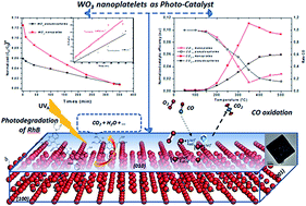
Two-dimensional nanoplatelets of tungsten trioxide (NP-WO3) were synthesized at room temperature, using a wet chemical method, without any surfactants or templates; aqueous mineralization was obtained by simply adjusting the pH. The resulting nanostructures were characterized using X-ray diffraction combined with Rietveld refinements, Raman and UV-Vis spectroscopies. Their morphologies and sizes were analyzed by scanning and electron microscopies. The electrical, optical, catalytic and photocatalytic properties of the NP-WO3 nanoplatelets were then determined and compared to the ones of pseudospherical (PS-WO3) standard samples. Nanoplatelets as well as pseudospherical particles crystallized in the single orthorhombic WO3 phase. The Rietveld refinement calculations and HRTEM analyses revealed a strong distortion of the WO6 octahedra, according to the W–O splitting. The electrical conductivity of WO3 compact pellets showed that both samples were semi-conducting with a weak difference in activation energies. Using a homemade photocatalytic device, the NP-WO3 particles used as photocatalyst in an aqueous medium, exhibited a significant efficiency to decompose rhodamine B over their large exposed surface (010), compared to PS-WO3 particles. These NP-WO3 particles were also used as the catalytic material for oxidation in an air–CO gas flow. They exhibited catalytic activity higher than the one in the PS form.


I. Introduction

In recent years, various studies have clearly demonstrated the relevance of certain chemical syntheses to control the sizes and morphologies of nanomaterials, both in basic science and in industrial applications. The nanoparticles having low dimension morphologies, 1D and 2D, can present physical and chemical properties strongly differing from the ones of bulk materials. They can be utilized as high effective catalysts, and applied in nanodevices for electronic, magnetic, and optical applications.1–7

Tungsten trioxide WO3 is an important n-type semiconductor with high stability and wide tunable band gap, around 2.6 eV at room temperature.5,8,9 The gap of the structure is depending upon bonding–antibonding W–O interaction, which correlating to the overlap in each direction. As a semiconductor material, WO3 has a broad range of potential applications in various fields such as photocatalysis, heterogeneous catalyst,10,11 gas sensor,12 electrochromic devices,13 water splitting to produce H2 and O2 (ref. 14) and solar energy devices.15 The properties of WO3 are critically dependent on structure, size and morphology.16 Therefore, a great effort has been devoted to synthesize tungsten oxide with well controlled shapes and defined sizes with powerful performances. WO3 has many polymorphs depending on the synthesis method and the temperature range. The idealized structure of WO3 is cubic, with a three dimensional network of corner sharing octahedra. The polymorphs correspond to more or less distortions of this network, tilting of the octahedra or cation displacements, which lead then to different crystallographic structures of WO3.17 At temperature ranges between ambient and 500 °C, the monoclinic and orthorhombic phases are predominant.

In order to control the morphology and size of tungsten oxides, many efforts have been devoted to the syntheses route. Several methods were developed to obtain different morphologies of WO3 such as hydrothermal reaction,18 template assisted methods,19 chemical vapor deposition20 and electro-deposition.21 Tungsten oxide with particular grain shapes has been obtained, including one-dimensional nanoscale building blocks22 and other advanced shapes such as flower-like,23 urchin-like24 and hierarchical hollow architectures.25 In this case, Gimeno-Fabra et al. obtained tungsten oxide nanoplates using near- and super-critical water in a continuous flow system with tungsten(VI) ethoxide as precursor and calcination temperatures above 350 °C.26 Gehong Zhang et al. fabricated WO3 nanosheets of ∼200–500 nm via a fast and organic additives-free hydrothermal method.27 These methods require, however, complicated operating procedures and/or the addition of various surfactants, for a better control of the morphology. However, it is still a significant scientific challenge to develop simple and reliable synthetic methods with controllable morphologies and uniform sizes through mild and low cost chemical routes.

Among various nanostructures, two-dimensional inorganic nanomaterials have attracted considerable attention because they could offer new opportunities in applied surface materials. The 2D sheet structure generally exhibits high surface energies, provide active sites for catalysts and sensors and can be used as building blocks to construct complex nanostructures.28 In addition, due to their huge light exposed surface area, they show supreme advantages for photocatalysis compared to the 1D and 3D counterparts.27

In this work, we present for the first time a well-controlled synthesis of orthorhombic quadrangular nanoplates of WO3 (called NP-WO3), using a mineralization process free from any one-step template, without addition of surfactant. We compare the properties of these nanoplatelets to the ones of WO3 powders having pseudospherical form (called PS-WO3) and considered as standard samples. The samples were characterized by X-ray diffraction (XRD) and Raman spectroscopy. The morphological and local observations were obtained from scanning electron microscopy (SEM), transmission electron microscopy (TEM), high resolution transmission electron microscopy (HRTEM) coupled to the energy dispersive X-ray spectroscopy (EDS). Finally, a systematic comparison between the properties of the NP and PS WO3 samples was undertaken, with the studies of the electrical conductivity, the catalytic activity in presence of CO gas, the energy gap determination and finally the photocatalytic activity in presence of rhodamine B, in aqueous solution.

II. Experimental setup

1. Synthesis and structural characterization

The NP-WO3 particles were synthesized using sodium tungsten Na2WO4·2H2O as precursor by a simple free template precipitation method. In a typical synthesis, a given amount of precursor was dissolved in a 20 mL of distilled water under continuous stirring, and HCl (2 M) diluted solution was added until the formation of pale yellow precipitates. The solid was transferred into 60 mL of diluted HCl solution (2 M). After continuous stirring for 24 h, the mixed solution was aged at 80 °C for 96 h. The yellow precipitate was filtered, washed with distilled water several times and finally calcined at 500 °C for 2 h in air, with a heating rate of 5 °C min−1.

The PS-WO3 powders were synthesized by dissolving 6 g of ammonium tungstate hydrate (NH4)10(W12O41)·6H2O in 30 mL of absolute ethanol solution. 3 mL of HNO3 was added to the solution and then stirred by a magnetic stirrer at 70 °C.29 The solution was heated until the solvent was evaporated. The yellow precipitate was filtered, washed with distilled water, dried at 80 °C. The obtained sample was annealed at 500 °C for 2 h in air with a heating rate of 5 °C min−1.

The morphological characterizations of the powder were conducted by Scanning Electron Microscope (SUPRA 40Vp Colonne Gemini Zeiss SEM operated at 10 kV) and Transmission Electron Microscope (Tecnai G2 operating at 200 kV, with a point to point resolution of 0.25 nm). The crystal structure of WO3 was determined via X-ray diffraction XRD (EMPYREAN Panalytical diffractometer) with a Cu Kα source. X-ray patterns were compared with those of the International Centre for Diffraction Data (ICDD). The DBWS 2.16 software was used to refine the structural parameters of the different products.30,31 The crystal cell parameters of the as synthetized materials were calculated from the Rietveld method. The program uses the Newton–Raphson algorithm to refine and quantify the intensities and profile of the peaks. Diffraction peak profile adjustment is performed using the modified pseudo-Voigt function containing the mixtures of Lorentzian and Gaussian contributions. The minimization was carried out using the reliability index parameters such as the Bragg factor (RBragg), comparing to the calculated and observed intensities (Ical and Iobs), the expected factor (Rexp), the weighted profile factor (Rwp) and the goodness of fit χ. All these parameters were used as numerical criteria of the quality of refinement calculations. From the optimized profile, we used the Debye–Scherrer (DS) approach to calculate the particles size using the following relationship:32–34

 
image file: c6ra13500e-t1.tif(1)
where D is the crystallite size, K is the form factor (K = 0.9 in the case Gaussian profiles), λ is the X-ray radiation wavelength (λ = 0.15406 nm), Δ(2θ) is the angular broadening of Bragg peaks resulting from the size effect and θ is the Bragg angles in radians. The integral breadth β value was calculated using a Gaussian approximation of peak profiles such as β2 = Δ(2θ)samp2 − Δ(2θ)stand2. Δ(2θ)samp and Δ(2θ)stand are respectively the full width at half maximum (FWHM) of Bragg peak of the synthesized samples and the standard WO3 sample obtained after a thermal treatment of 24 h at 600 °C. The difference Δ(2θ) is the broadening resulting from size effect. A theoretical specific surface area SA was calculated using the approximation of particles having the form of square sheets, with an average thickness e, an average linear side size l, and having a density ρ (7.28 g cm−3):
 
SA = (1/e + 2/l)2/ρ (2)

To highlight the efficiency of the morphology, we compare the studied properties of the nanoplatelets to the pseudospherical nanoparticles. In the case of spherical particles, we use the classical formula35 of the specific surface area: SA = 6/ρd where d is the mean particle diameter (or coherence length). The apparent size (e, l and d) were determined from SEM and TEM images. Considering the NP geometry with defined dimensions (l and e), the percentage τ of each facet can be calculated as following: image file: c6ra13500e-t2.tif, where Si is the surface area of the i facet.

Raman spectroscopy was used to analyze the characteristic vibration modes associated to the bonds present in the obtained material according to the constituent's element. The equipment used to record the various vibration spectra was a spectrometer Horiba Jobin-Yvon HR800 LabRam, spatially resolved to 0.5 microns, by means of an optical microscope with a 100× objective. The 514.5 nm line of an Ar-ion laser was used as the excitation source; the photonic power applied to the samples was limited to 5 μW with an acquisition time of 30 seconds.

2. Properties

Optical analysis. The analysis of UV-visible diffuse reflectance spectra (DRS) of the different samples has been done using a LAMBDA 190s UV/Vis/NIR spectrometer along with 150 mm integrating sphere. A small volume powder sample was manually pressed into a 3.2 cm powder cup which was clamped (attached) on the external port of the integrating sphere. The measures were performed in the range of 250–800 nm at room temperature. The baseline was carried out using a calibrated spectral on reflectance standard.

Raman spectra were obtained using a spectrometer Horiba Jobin-Yvon HR800 LabRam, spatially resolved to 0.5 μm, by means of an optical microscope with a 100 objective.

Electrical analysis. The electrical measurements were performed using electrical impedance spectroscopy (EIS) under air at atmospheric pressure, in the same temperature range explored in catalytic experiments. The SOLATRON (SI 1260 AC) impedance analyzer was used in the frequency range of 1 to 106 Hz. For a given temperature, each measurement was recorded after stabilization of the heating process. The samples were compacted in the form of pellets at a pressure of 4 kbar, and then placed between two cylindrical platinum electrodes.
Catalytic properties. The catalytic studies were performed using a homemade device allowing the reaction of a powder catalyst with a gas flow containing a gas to be oxidized, at a fixed temperature. The product resulting from the gas–solid interaction was analyzed by Fourier Transform InfraRed spectroscopy (FTIR, Bruker-Tensor 27), coupled to a quadrupole mass spectrometer (MS, MKS – CIRRUS). This study was conducted with 1250 ppm of CO diluted in air and FTIR spectra were acquired every 30 s. For further information, the details of the experiment are reported in a previous work.36
Photocatalytic activity. The photocatalytic activity of samples was characterized from the UV irradiation of aqueous solutions in which rhodamine B (RhB) and NP or PS active particles of WO3 were present at fixed concentrations and at a stabilized temperature. The degradation of RhB was observed under UV light using an 80 W mercury lamp, operated at 254 nm (or 4.88 eV). For this purpose, 250 mg of WO3 powders was dissolved in 250 mL of RhB (10 mg L−1) and then exposed to ultrasound for 5 min to eliminate aggregates. Prior to the irradiation, the suspension was stirred for 60 min in darkness to reach an adsorption–desorption equilibrium. After this time, the light source was turned on. During the reaction, samples were taken from the reactor at different time intervals. Given their low values, the concentrations of RhB in these irradiated solutions can be considered as proportional to the observed intensity of the RhB absorption peaks at 554 nm. Thus, the degradation rate of RhB was analyzed using a UV-visible spectrophotometer (Shimadzu UV-24646) and expressed as Cn/C0, where Cn is the concentration of RhB for each irradiated time, and C0 is the initial concentration.

III. Results and discussion

1. Structural and morphological characterization

The synthesis method leads to well crystallized grains for both samples, though with different morphologies. The SEM images show that the powders consist either of large quantity of platelets (Fig. 1a) and particles without shape that can be considered as pseudo-spherical grains (Fig. 1b). The images show also that the grains with different morphologies tend to form a dense aggregate, particularly for PS particles. The insert TEM images show a quadrangular NP-WO3 with a mean lateral size of 175 nm and an average thickness of 40 nm. The PS-WO3 grains are smaller than the nanoplatelets, with a size distribution centered on 60 nm. The platelet sample presents a relative uniform size distribution compared to the pseudospherical powder.
image file: c6ra13500e-f1.tif
Fig. 1 SEM images of the WO3 powders: (a) NP-WO3 and (b) PS-WO3. The TEM pictures in insert show the size dispersion of the grains.

Fig. 2 shows the XRD patterns of the samples. Both patterns correspond to well crystallized tungsten oxide phase. The observed Bragg peaks of the diffractograms are characteristic of a single phase WO3. Moreover, no characteristic residual peaks from other crystalline impurities were detected. At the synthesis temperature used, WO3 can be either monoclinic or orthorhombic,37 with very closed lattice parameters. Thus, Rietveld refinements were done with the γ-WO3 monoclinic structure P121/C (no. 14)38 as well as the β-WO3 orthorhombic phases Pnma (no. 62)37 and Pmnb (no. 60).39


image file: c6ra13500e-f2.tif
Fig. 2 Rietveld analyses (space group Pnma no. 62): observed and calculated XRD profiles of the structures: NP-WO3 and PS-WO3.

The refinement is significantly better with the orthorhombic structure (reliability factors Ri < 10%) compared to the monoclinic phase. The results of the Rietveld refinements are summarized in Table 1, where the refined lattice parameters are reported. The initial atom coordinates have been exported from CIF datasheet of WO3 (836-ICSD database) structure which has a low shift of Bragg peaks compared to our experimental diffraction patterns. According to the Debye–Scherrer calculation, we obtained a mean size of 64.3 (±1.0) nm and 82.9 (±1.0) nm for NP-WO3 and PS-WO3 respectively.

Table 1 Refinement structural parameters and coordinates atoms of WO3 phase based on two octahedra structure (space group of Pnma). Refinement calculation based on CIF datasheet of ICSD (collection code 836)
Coordinates x y z x y z
Atoms Nanoplatelets Pseudospheres
W1 0.0276(1) 0.2500(0) 0.0260(5) 0.0276(0) 0.2500(0) 0.0285(4)
W2 0.0289(0) 0.2500(0) 0.5375(0) 0.0259(5) 0.2500(0) 0.5355(6)
O1 0.00000 0.00000 0.00000 0.00000 0.00000 0.00000
O2 0.00000 0.00000 0.00000 0.00000 0.00000 0.00000
O3 0.00000 0.00000 0.50000 0.00000 0.00000 0.50000
O4 0.00000 0.00000 0.50000 0.00000 0.00000 0.50000
O5 0.2573(3) 0.2500(0) 0.0633(1) 0.2598(3) 0.2500(0) 0.0565(1)
O6 0.2517(3) 0.2500(0) 0.5025(9) 0.2646(4) 0.2500(0) 0.5055(5)
O7 0.0324(8) 0.2500(0) 0.2458(7) 0.0522(5) 0.2500(0) 0.2460(8)
O8 0.004759 0.2500(0) 0.7792(1) 0.0003(0) 0.2500(0) 0.7719(7)
Structural parameters a = 7.5347(5) Å; b = 7.3131(3) Å; c = 7.6941(9) Å, α = γ = β = 90.0° a = 7.5239(0) Å; b = 7.3222(7) Å; c = 7.6892(2) Å, α = γ = β = 90.0°
Reliability factors Rp = 9.589%; Rwp = 12.668%; Rexp = 6.122%. Goodness of fit χ2 = 4.280 Rp = 7.962%; Rwp = 10.297%; Rexp = 6.728%. Goodness of fit χ2 = 2.169


Due to the specific Wyckoff positions, the coordinate's atoms were fixed to start the refinement procedure. We first refined the W coordinates then those oxygen atoms of the WO3 structures (due to their low scattering factors). The refinements were carried out with orientation factors, anisotropic and isotropic respectively for platelets and pseudospheres. Moreover, the difference between XRD pattern profiles associated with each morphology can be related to the degree of crystallization and to the local order of atoms. The refinement position gave set structural parameters with low deviation, but sufficient to distinguish the two structures. According to the of XRD pattern profile, the samples show different textures, which characterized by different intensities of the main peaks at 23.10°, 23.59° and 24.32° corresponding to (002), (200) and (020) plans. For the isotropic pseudospheres the intensities are similar, but for nanoplatelets, we obtained a higher intensity for (020) orientation than (002) and (200), confirming the anisotropic form.

The obtained refinement parameters were exploited by Carine software for the cell representation. The crystal structure of orthorhombic WO3 is shown in Fig. S2 (ESI). The schema presents a multilayer configuration of alternating octahedral groups WO6 connected in three space directions, which the atoms of W are located in the center of the octahedra and oxygens are at the vertices, thus each oxygen is forming a connection W–O–W.

Using Carine software and our refinement results, we extracted the main bond lengths and bond angles, reported in Table 2. It should be noted that the refinement was occurred with a multiplicity of order two (two octahedra Oct1 and Oct2), according to the agreement phase datasheet.

Table 2 Selected bond distances and angles in different nanostructure of WO3, with two optimized WO6 octahedral of the unit cella
WO6 octahedra groups Nanoplates Spheres
Oct1 Oct2 Oct1 Oct2
a Multiplicity; a, b and c indicate the three direction.
W–O bond (Å) error: 0.072 Å Axes  
a 1.692 1.700 1.683 1.811
1.754 1.864 1.760 1.828
b 1.851 1.864 1.855 1.861
1.851 1.869 1.855 1.861
c 1.907 2.188 1.983 2.124
2.090 2.244 1.996 2.235
O–W–O angle (°) 78.8 70.0 76.5(2) 76.0
79.4 80.2 82.6(2) 77.6
82.9(2) 80.6(2) 82.7(2) 81.5(2)
83.2(2) 81.2(2) 97.2(2) 82.1(2)
96.4(2) 95.2(2) 97.5(2) 94.9(2)
97.3(3) 98.0(2) 102.9 97.8(2)
104.6 104.9(2) 103.9 103.4(2)
162 150.1 161.3 153.2
176.1 157.6 179.6 159.2
176.6 175.1 179.5 179.0
O–O bond (Å) error = 0.055 Å 2.496 2.631 2.535 2.609
2.496 2.631 2.535 2.609
2.616 2.634 2.547 2.705
2.616 2.634 2.547 2.705
2.642 2.688 2.662 2.705
2.642 2.688 2.662 2.705
2.709 2.821 2.713 2.779
2.709 2.821 2.713 2.779
O–O corner distance (Å) Axes  
a 3.840 3.760
b 3.660 3.660
c 3.600 3.670
W–W distance (Å) a 3.79 3.81
b 3.70 3.71
c 3.94 3.79


In this case, we obtained a layered structure based on the alternating and distorted octahedra WO6. In WO6 regular octahedrons, two chemical bonds are perpendicular to a plane in which the four other chemical bonds are located. In the present structures, the two shorter bonds vary but are closed to 1.7 Å for Oct1 and Oct2. The four longer bonds strongly vary in the range 1.99 to 2.23 Å, for Oct1 and Oct2. The O–O distances to the vertices between nearest neighbors, vary slowly from 2.49 to 2.78 Å. The O–O corner distances of the octahedra vary from 3.6 to 3.84 Å while the W–W distance reaches 3.95 Å: all these values characterize flat irregular octahedra. These distortions were also observed with the variation of O–W–O angles, as summarized in Table 2.

Generally, WO3 exhibits a perovskite structure even in the orthorhombic phase at higher temperature. So, the irregular bond distances and angles of polyhedron are at the origin of the deformation and distortion. For both samples, the W positions shift from the midpoints of the octahedral to form zigzag chains in the a and b directions. In this case, the orthorhombic system shows alternation of long and short W–O bonds in both the a and c directions, but not in the b direction. However, the splitting in c direction is larger for platelets than spheres octahedral.

The transmission electron microscopy images and associated electron diffraction patterns showed that each nanoplatelet is a single crystal. Most encountered platelets appear as square, although rectangular ones can also be found (Fig. 3b). When the nanoplatelets lay flat, the corresponding zone axes show a quadratic symmetry for the strong spots, remaining of the ideal cubic structure of WO3. Fig. 3a and c can be distinguished by their superstructure spots (with regards to the cubic structure). Fig. 3a shows weak superstructure spots along two perpendicular directions as Fig. 3c has strong superstructures spots along one direction. These supplementary spots could only be indexed in the orthorhombic β-WO3 phase with space group 62 (Pnma), with two perpendicular zone axes [010] and [001] respectively. Nanoplatelets laying edge on brought information along the growth direction of the platelets. Again, the strong spots of the diffraction patterns (Fig. 4a and b) exhibit a quadratic symmetry, showing that the zone axis is perpendicular to those of Fig. 3a and c. The weak superstructure spots could be indexed in the β-WO3 structure and Fig. 4a and b correspond to [100] zone axis. Depending on the platelets, more (Fig. 4b) or less streaks (Fig. 4a) along b* can be observed in the diffraction patterns, indicating defects in the piling up of (0k0) planes, thus along the main growth direction of the nanoplatelets. HRTEM images taken along the same zone axis show the irregular piling up of (0k0) planes (Fig. 4c). Variations of more than 10% of the interreticular distances were measured. Dislocations are revealed in the inverse fast Fourier transform (Fig. 4d) (HRTEM images and diffraction patterns are in ESI).


image file: c6ra13500e-f3.tif
Fig. 3 TEM image and electronic diffraction patterns of flat laying WO3 platelets: (b) image of the dispersed nanoplates, (a) and (c) correspond respectively to perpendicular [010] and [001] zone axes of the orthorhombic β-WO3 structure.

image file: c6ra13500e-f4.tif
Fig. 4 HRTEM image and electron diffraction patterns of WO3 platelets laying edge on: (a) and (b) correspond to the [100] zone axis of the orthorhombic structure, (c) is an HRTEM image showing the piling up of (020) planes. The inverse fast Fourier transform (d) emphasizes the defects in the piling up of the plans, pointed by arrows.

According to the obtained results (Table 2), the interreticular distance can be identified as the heavy atoms distances W–W and they vary in three directions. So, the measured distance from the HRTEM image (Fig. 4c) in the c direction is in agreement with that deduced from refinement calculations: 3.94 Å. Based on the above TEM observation and structural analysis, we conclude that the top and bottom facets are (010) and lateral facets are (100) and (001). From Fig. S2b (ESI), we can see that (010) facets of the orthorhombic structure are O terminated planes. Compared with the (010) facets, there are more W atoms exposed on the surfaces of (100) and (001) planes (Fig. S2a and S2c). It's indicated that the (010) plan have more active oxygen sites. Therefore, the anisotropic property of the nanoplatelets will exhibit different physical/chemical properties than isotropic PS-WO3.

Raman analysis. According to previous research,40–42 the Raman activity of phonons is caused by the successive deformation of the ideal cubic lattice. Most peaks below 200 cm−1 are usually attributed to lattice modes, whereas the mid and high frequency regions correspond to deformation and stretching modes, respectively. Since inorganic compounds have vibration bands mainly below 1200 cm−1, an investigation of Raman spectroscopy of WO3 show mainly seven vibration bands in range of 50–1000 cm−1, as reported in Fig. 5. In the range of 50 to 150 cm−1, we observe a typical characteristic peaks of the orthorhombic crystalline phase at low frequencies, which are associated to lattice vibrational modes.43–45 The peaks at 273 and 330 cm−1 are assigned to the bending vibration O–W–O.44,46
image file: c6ra13500e-f5.tif
Fig. 5 Raman spectra of WO3 structures.

The bands in the range 700–850 cm−1 are attributed to either the antisymmetric stretch of W–O–W bonds or the symmetric stretch of O–W–O bonds.47,48 Thus, the intense peaks centered at 808 and 718 cm−1 are typical Raman peaks of crystalline phase of WO3, which correspond to the stretching vibrations of the bridging oxygen43,49 and these are assigned to W–O stretching (ν), W–O bending (δ) and O–W–O deformation (γ) modes, respectively.46,50 Close to the high frequency Raman bands of PS and NP samples, we also observe large undulations with two different aspects in PS and NP samples (maximum close to 640 nm): this could be ascribed to specific defects in the lattice, probably linked to a non-stoichiometry in oxygen associated with local distortions. In addition, the two high-frequency Raman bands of NP-WO3 particles are characterized by thinner profiles and higher maximum compared to the ones of PS-WO3 particles. These observations are correlated with the different profiles of the low frequency bands (lattice modes). In this case, the absorption band at 135 nm is higher for PS particles. As reported in the Table 2, the W–O bond is smaller for PS particles (1.68 Å) than NP, which the shorter bond rather promotes more overlap orbitals.

Generally, these differences observed for PS and NP samples could be due to a better crystallization level coupled to the anisotropy of the platelets for the NP samples. Taking into account to the WO6 distortions and the presence of the linear defects in the plane of the plates, nanoplates present deformation and stretching modes more intense than pseudospherical, in agreement to the bonds and angles changes deduced from XRD-refinement and observed defects from HRTEM images.

2. UV-Vis diffuse reflectance

As the values of optical band gap energies generally condition the photocatalytic activity of materials, it was necessary to characterize the influence of morphology on optical properties of the as prepared NP and PS WO3. Let us recall that the current values of band gaps of WO3 materials are found to be close to 2.6 eV. The UV-visible diffuse reflectance spectroscopy (DRS) at room temperature was used to determine the band gap energies, noted Eg, of NP and PS WO3.

The intrinsic absorption edge of the powders can be evaluated and discussed in terms of the indirect interband transition. The optical energy band gap is obtained by using the Kubelka–Munk method.51 This method consists in plotting F(R) versus photon energy and extracting Eg by a linear fit (see Fig. 6). R designates the absolute reflectance of the sample at infinite thickness and F(R) is the conversion of the diffuse reflectance measurements R to F(R) according to the following equation:

 
image file: c6ra13500e-t3.tif(3)
where R designates the absolute reflectance of the sample at infinite thickness. K represents the molar absorption coefficient and S is the scattering coefficient. F(R) of the different samples treated at 500 °C, are plotted in Fig. 6. It is expected to show a linear behavior in the higher energy region, which should correspond to a strong absorption near the absorption edge. Using linear fitting method, extrapolating the linear portion of this straight line to zero absorption edge gives the optical energy band gap of the powders.


image file: c6ra13500e-f6.tif
Fig. 6 Variation of F(R) as a function of irradiation energy, for the PS and NP samples, R being determined from UV-Vis absorbance spectra.

The band gap absorption of the WO3 with two morphologies was estimated to be 2.65 and 2.82 eV for pseudospheres and nanoplatelets, respectively. The difference between the gap can be attributed to different factors such shape, crystallite size,52 lattice parameters,53 degree of structural order–disorder in the lattice and the Moss–Burstein effect.54–56 The change of these factors depends on the distortion polyhedra as mentioned in the Table 2, which the bond length and angles vary from one morphology to another. In our case, it should be remarked that the band gap of NP particles is greater than the one of the PS particles: this could be ascribed to the difference in morphology and sizes of particles, keeping in mind that strong anisotropy and smaller sizes are observed for the NP particles. It is well known that the band gaps Eg generally increase as crystallite sizes decrease, in the case of semiconducting particles.52

Moreover, the electronic structures of pure WO3 phases may be interpreted in terms of W–O bond splitting, i.e. different bond length in the same direction. As reported by Chatten et al.,8 the presence of W–O bond splitting induces an increase in the band gap though the magnitude of the splitting in the three directions. In the case of the orthorhombic phase, the structure show fairly strong splitting in two directions. The magnitude of the band gap in our materials is dominated by the splitting in the c direction (1.907 to 2.244 Å) and also splitting in a direction (1.692 to 1.864 Å), in the same order to those obtained by DFT calculation. According to the data of the Table 2, the splitting is higher for NP than PS oxides, therefore a large gap for NP 2.82 eV. This behavior resulted in shorter W–O bond, increased overlap of O 2p and W 5d and increased bonding–antibonding interaction.57

3. Electrical impedance spectroscopy

Electrical measurements were obtained with a series of Nyquist representations for the optimized WO3 sample as a function of temperature. To interpret the semicircles of Fig. 7a, a specific electrical equivalent circuit was used to fit the experimental data. This involved a resistance R in parallel with a constant phase element ZCPE corresponding to the form ZCPE = (JAω)n; where A has the dimension of a capacity (Farad) only for n = 1:
 
1/Z = 1/R + (JAω)n (4)

image file: c6ra13500e-f7.tif
Fig. 7 (a) An example of Nyquist representation of the electrical impedance obtained for NP-WO3. (b) Conductivity σ of the samples as a function of the reciprocal temperature.

Generally, the exponent n characterizes grain heterogeneity and sample porosity. In the case of heterogeneous samples having a large distribution of grain sizes, the n values are lower than 1. However in the case of ionic diffusion and reaction, this CPE model could be used to represent the electrical signals in competition with the classical Warburg model mainly valid to represent diffusion at the electrodes.58 The obtained results show a unique main semicircle for both samples corresponding to grain core electrical behavior, as reported in the Fig. S5 (ESI). In the case of the nanoplatelets (Fig. S5a and S5d), a linear segment appears at a lower frequency, suggesting a typical Warburg-like behavior corresponding to electrodes signals. It should be recalled that, as the electrodes are metallic (Pt), they allow electron conduction, and behave as blocking electrodes for ionic conduction. In fact, the observation of such a signal is generally attributed to gas interaction with electron exchange at the electrodes. This is probably linked to the common reactions: O + e ↔ O and/or ½O2 + 2e ↔ O2. We also note that the diameter of the semicircles decreases according to the temperature. The linear segment disappears between 150 and 350 °C. At low temperature, the Warburg behavior is due to the adsorption and desorption of gases (oxygen and water molecules). However, at high temperature, the Warburg behavior is mainly caused by the conduction and the accumulation of electrons on the electrode surface.

The intersection of the semicircles and the horizontal axis Z′ corresponds to the R value. The temperature dependent activation energies have been calculated from the Arrhenius plot of data using the following equation:

 
image file: c6ra13500e-t4.tif(5)
where Ea is activation energy for conduction, K a pre-exponential factor and T the sample temperature in Kelvin. In this expression, the conductivity σ is obtained from the classical relation: σ = l/RS, where l and S are respectively the thickness and surface of cylindrical pellet in contact with electrodes. This conductivity depends on effective porosity and microstructure of the compacted pellet. It should be noted that this expression is only valid for pure electron conduction, and is generally used as a good approximation in the case of mix conduction. In fact, it was necessary to determine these activation energies in various temperature ranges. These variations of activation energies could be associated with electrical evolutions involved by lattice expansion or charges carriers modifications in solids. The activation energies have been calculated taking into account the total resistance R.

Fig. 7b shows the evolution of the logarithm of conductivity as a function of the reciprocal temperature. The conductivity curves can be divided into two parts depending on the temperature. At low temperature, we observe a first increase of log(σ) as T increases up to 75 °C: this can be associated with extrinsic transport of impurities including adsorbed gases. Then we observe a strong decrease of conductivity due to gas desorption and water molecules elimination up to 125 °C for PS sample and up to 200 °C for NP sample. The desorption process is faster for an isotropic system PS as compared to anisotropic nanoplatelets. Finally, the conductivity increases again, following a classical semiconductor behavior. Close to 300 °C, it appears a small change in slope, giving rise to a continuous electrical modification. This particular trend can be due to a modification in charge carriers (the intrinsic carriers playing a prominent role at high temperature) or to a structural transformation. A similar phenomenon has been reported by other group for dc resistance measurement of pure WO3.59,60 They have explained this change by a monoclinic → orthorhombic WO3 phase transition.61,62

The electrical transition could be associated with lattice expansion or charges carriers modifications in solids. The activation energies have been calculated taking into account the total resistance R. In Table S1 we have reported the activation energies at each step. At high temperature (T > 500 K), the activation energies can be connected with the formation of intrinsic defects (Schottky defects, oxygen vacancies) in the bulk. At low temperature T < 400 K, extrinsic defects resulting from adsorbed molecules or impurities from initial constituents, are dominant in transport properties. If the material is subjected to air atmosphere, the exchange with oxygen plays the major role in the composition of the solid at high temperature and its non-stoichiometry.

4. Catalytic applications

CO oxidation. Catalytic analyses were carried out by FTIR spectra acquisitions, every 30 s. In presence of active samples, the spectra are characterized by the appearance of a new absorption band corresponding to the emission of CO2 resulting from CO conversion, following the well-known conversion reaction CO + ½O2→ CO2.

Fig. 8a and b represent the time dependent evolutions of the CO2 FTIR band intensity at various temperatures, for NP-WO3 sample (data of PS-WO3 are in ESI). The decrease in CO band intensities is clearly correlated with the increase in CO2 band intensities. At 350 °C, the conversion reaches a maximum level (the CO band increases and the CO2 band reaches a maximum value) for NP. The solid–gas interactions are based on three main physicochemical steps: gas adsorption process, surface reactions and gas desorption process. This process was relative to reactions between adsorbed CO gases and adsorbed oxygen (O2) from air, an interaction described by the Langmuir–Hinshelwood mechanism.63


image file: c6ra13500e-f8.tif
Fig. 8 Catalytic activity of WO3 nanoplatelets versus time. Evolution of the intensities of FTIR absorption bands: (a) CO oxidation into (b) CO2.

The calculation of the surface area of the two NP and PS samples based on the XRD size effects (D values) delivered the values of 9 m2 g−1 for NP sample and 14 m2 g−1 for PS sample. According to these values, the (010) facets contribute about 70% of the surface area with respect to other facets. From these data, the catalytic efficiencies can be expressed per surface unit. As temperature increased, CO conversion occurred up to a maximum of oxidation activity. Fig. 9 reports the catalytic efficiency, normalized to the specific surface of each sample. These data clearly show that the conversion efficiency strongly increases for nanoplates than pseudospheres and remain stable until 500 °C. The catalytic performance of the platelets is at least two times higher than the spheres particles.


image file: c6ra13500e-f9.tif
Fig. 9 Normalized catalytic efficiency to the specific surface area.

Generally, the catalytic activity can be attributed to any increase in specific surface of samples, which is not the case for our samples. The catalytic reactivity normalized to the surface unit may be linked both to the morphology and the nature of exposed surfaces. As reported by ab initio calculation, the plan platelets (020) exhibit more active oxygen sites than other plan orientations, as shown by Fig. S2b.64 However, orientation (200) and (002) present a surface state conditioned by a mixture of sites of W and O atoms, thus less reactive. Therefore, the pseudospherical particles are more isotropic with equal distribution of active sites. As a consequence, they show less oxygen sites than nanoplates.

So regarding the electrical behavior, the conductivity of the fabricated WO3 samples increased with temperature, mainly due to high mobile electrons. For the same temperature range, the catalytic conversion of CO into CO2 was improved. The conduction is due to the charge carrier displacement in the oxide grains and occurs through the barriers at the generated interfaces. The increased capacity to exchange electrons with external molecules (CO and O2) of the anisotropic microstructure of thin platelets is at the origin of this improved conversion of CO into CO2.

Analyzes of the used samples after catalytic applications, show no structural changes. In addition to the general appearance of the powder, unchanged color, the samples were checked by XRD. A slight decrease of the peak intensities was observed, however the Bragg position remain identical (Fig. S1 of ESI), thus demonstrating the stability of the oxides. This stability is enhanced by the presence of air as an oxygen source for the regeneration of the active sites.

Photodegradation of RhB. The photocatalytic activities of nanoplates and pseudospherical oxides were evaluated from the degradation reaction of RhB in aqueous solution, under UV irradiation. Irradiation in the absence of WO3 samples shows that the degradation of RhB is extremely lower, lower than 5% during the experiment time. Fig. 10 shows the absorption spectra of the RhB solution for different times during UV lights irradiation in the presence of the catalyst. The characteristic peak intensity of RhB at 554 nm decreases progressively with irradiation times and the absorption peak almost disappears after 350 min irradiation for WO3 nanoplatelets, but still persists for the WO3 pseudospheres at the same irradiation time. The shift of the main absorbance band from 554 nm to 520 nm with irradiation time indicates the removal of ethyl groups one by one.65 Photocatalysis of RhB occurred under UV irradiation until complete degradation without altering the morphologies and powders remain yellow.
image file: c6ra13500e-f10.tif
Fig. 10 Absorption spectra of RhB solution with photocatalyst NP (left) and PS (right) of WO3 under UV irradiation.

As observed in Fig. 11, the photocatalytic efficiency of NP-WO3 and PS-WO3 reaches 93% and 87% respectively after irradiation for 350 min. The photodegradation rate constants k for the two catalysts were estimated from first-order reaction kinetics by using the classical relationship Cn/C0 = exp(−kt). The reaction rate constant are k = 0.0072 min−1 for NP-WO3 particles and k = 0.0050 min−1 for PS-WO3 particles (see insert Fig. 11). The higher photocatalytic activity observed for NP-WO3 particles can be ascribed to the large active surface areas (70% of SA), with large quadrangular faces (010) absorbing more UV light, small thicknesses allowing easy migration of electron–hole pairs to the surface, and more active adsorption and photocatalytic reaction sites.66


image file: c6ra13500e-f11.tif
Fig. 11 Normalized photocatalytic activity (Cn/C0)*. The insert corresponds to the Y = −ln(Cn/C0) function of time t delivering the constant k: k = 0.0072 min−1 for NP-WO3; k = 0.0050 min−1 for PS-WO3, correlation coefficient R = 0.976.

The absence of new absorption band during the reduction of RhB in the UV-Vis spectra (Fig. 10) indicates that RhB is decomposed thoroughly into CO2 and H2O according to the following mechanism.67 Under irradiation, photogenerated electrons would transfer from the valence band to the conduction band of WO3, allowing the formation of highly active electron–hole pairs according to the reaction WO3 + → h+ + e. The efficiency of this step depends particularly on the structural and electronic properties of the semiconductor.

Furthermore, the high platelet gap (2.82 eV) allows a longer residence time of the charge carriers in the conduction band, compared to spheres (2.65 eV). As a consequence, the photogenerated h+ and e then contribute to the oxidation and reduction reaction. The hole is quickly converted to the hydroxyl radical (OH*) upon oxidation of the adsorbed water. So, electrons most often react with dissolved O2 with formation of superoxide radical. They can further react and produce HO* radicals and thus contribute to oxidation of organic materials giving rise to water and CO2 gas. The formed hydroxyl radical is the major reactant, which is responsible for oxidation of RhB over WO3.68 The highest photodegradation of the nanoplatelets is due to their exposed crystal surfaces. Han et al.64 demonstrated that shape controlled WO3 nanocrystals with highly exposed (020) facets exhibit higher sensitivity compared to nanoparticles with other prominent facets or anisotropic particles. Similar trend was found in the case of TiO2 nanosheets and trapezohedron shaped In2O3 nanoparticles which exhibit high index facets.69,70

The differences in the photodegradation capability were attributed to the presence of unsaturated cations on the (020) surfaces, i.e. five and four-fold coordinated W ions, which could effectively chemisorb both oxygen species (e.g. O2, O2−, O) and the target molecules. Liu et al.71 indicated that the surface energy of crystal faces in shape controlled WO3 nanocrystals is in the following order of 1.56 J m−2 for (002) > 1.54 J m−2 for (020) > 1.43 J m−2 for (200) and suggested that (002) and (020) are the most active in surface mediated reactions.

A semiconductor with different crystal structures not only has different band gap but also has defects (as revealed for nanoplatelets) that can be affect the electron–hole recombination rate. Then, the reactivity of the photocatalyst is affected by both the morphology and the crystal structures.72 In addition to the state surface, the nanostructures with corners and edges as traps (like nanoplatelets) promote more adsorption than nanostructures without these traps (like nanospheres). Due to their low coordination numbers, corners and edges in the case of platelets or cubic shapes, have more catalytic activity in comparison with other flat surfaces, as reported by M. Farhadian et al.73 The NP-WO3 (with their corners and edges) in comparison to the PS-WO3 (with high surface area), have the most photocatalytic activity.

The photodegradation process is favored by the large surface area of the platelets, particularly the (010) facets (70% of the surface area), showing a high amount of catalytic reaction sites for the adsorption of reactant molecules and to more surface OH, therefore allows a high degradation rate of organic pollutant.

As reported in this last part of the CO oxidation, the oxides remain stable without color and structure alteration after rhodamine photodegradation. The XRD patterns occurs in a similar manner before applications.

IV. Conclusions

We have successfully synthesized well crystallized single phase WO3 platelets morphology, based on free template aqueous mineralization processes. The oxides were identified in the orthorhombic structure, close to monoclinic phase, with a large exposed (020) facet than (002) and (200). The microstructural analysis revealed the main orientation along the [020] plan with the presence of the linear defect parallel to (020). In addition, the distortion and deformation of the octahedra are critically dependent upon the W–O and O–O bonds. The splitting bonds are at the origin of the studied properties changes.

The photocatalytic performances of the as-prepared WO3 are investigated for the RhB degradation, which the photodegradation activity of nanoplatelets was significantly higher than WO3 with a spherical morphology. However, the CO transformation over tungsten material remains incomplete. According to the semiconductor behavior of the oxides, the CO oxidation based on the oxydo-reduction mechanism shows a favorable charge transfer for CO catalytic detection. The nanoplatelets morphology, with corners and edges, have the best catalytic activity in comparison with nanospheres. The large exposed (020) facets of the nanoplatelets show a high amount of catalytic reaction sites, for the conversion of reactant molecules and for photodegradation of organic pollutant with more surface OH.

Acknowledgements

The authors thank Pr. J. Ch. Valmalette for his assistance with the Raman measurements. We gratefully acknowledge the Regional Council of Provence-Alpes-Côte d'Azur, General Council of Var, and the agglomeration community of Toulon Provence Mediterranean for their financial supports in the framework of “M2D2” project.

References

  1. D. Chen, L. Gao, A. Yasumori, K. Kuroda and Y. Sugahara, Small, 2008, 4, 1813 CrossRef CAS PubMed.
  2. D. Chen, H. Wang, R. Zhang, L. Gao, Y. Sugahara and A. Yasumori, J. Ceram. Process. Res., 2008, 9, 596 Search PubMed.
  3. B. I. Kharisov, Recent Pat. Nanotechnol., 2008, 2, 190 CrossRef CAS PubMed.
  4. X. Shen, G. Wang and D. Wexler, Sens. Actuators, B, 2009, 143, 325 CrossRef.
  5. X. Li, G. Zhang, F. Cheng, B. Guo and J. Chen, J. Electrochem. Soc., 2006, 153, H133 CrossRef CAS.
  6. J. Su, X. Feng, J. D. Sloppy, L. Guo and C. A. Grimes, Nano Lett., 2010, 11, 203 CrossRef PubMed.
  7. D. Chen and J. Ye, Adv. Funct. Mater., 2008, 18, 1922 CrossRef CAS.
  8. R. Chatten, A. V. Chadwick, A. Rougier and P. J. Lindan, J. Phys. Chem. B, 2005, 109, 3146 CrossRef CAS PubMed.
  9. S. R. Bathe and P. Patil, Smart Mater. Struct., 2008, 18, 025004 CrossRef.
  10. M. Gondal, A. Hameed and Z. Yamani, J. Mol. Catal. A: Chem., 2004, 222, 259 CrossRef CAS.
  11. H. Liu, S. Huang, L. Zhang, S. Liu, W. Xin and L. Xu, Catal. Commun., 2009, 10, 544 CrossRef CAS.
  12. J. Ou, M. Yaacob, J. Campbell, M. Breedon, K. Kalantar-Zadeh and W. Wlodarski, Sens. Actuators, B, 2012, 166, 1 CrossRef.
  13. J. d. R. M. Neto, R. M. Torresi and S. I. C. de Torresi, J. Electroanal. Chem., 2016, 765, 11 Search PubMed.
  14. W. Zhao, Z. Wang, X. Shen, J. Li, C. Xu and Z. Gan, Int. J. Hydrogen Energy, 2012, 37, 908 CrossRef CAS.
  15. H. Zheng, Y. Tachibana and K. Kalantar-zadeh, Langmuir, 2010, 26, 19148 CrossRef CAS PubMed.
  16. M. Ahmadi, S. Sahoo, R. Younesi, A. P. Gaur, R. S. Katiyar and M. J. Guinel, J. Mater. Sci., 2014, 49, 5899 CrossRef CAS.
  17. C. Chacón, M. Rodríguez-Pérez, G. Oskam and G. Rodríguez-Gattorno, J. Mater. Sci.: Mater. Electron., 2015, 26, 5526 CrossRef.
  18. M. Szabó, P. Pusztai, A.-R. Leino, K. Kordás, Z. Kónya and Á. Kukovecz, J. Mol. Struct., 2013, 1044, 99 CrossRef.
  19. K. P. Musselman, G. J. Mulholland, A. P. Robinson, L. Schmidt-Mende and J. L. MacManus-Driscoll, Adv. Mater., 2008, 20, 4470 CrossRef CAS.
  20. S. Gubbala, J. Thangala and M. Sunkara, Sol. Energy Mater. Sol. Cells, 2007, 91, 813 CrossRef CAS.
  21. M. Deepa, A. Srivastava, S. Lauterbach, S. Shivaprasad and K. Sood, Acta Mater., 2007, 55, 6095 CrossRef CAS.
  22. F. Zheng, M. Zhang and M. Guo, Thin Solid Films, 2013, 534, 45 CrossRef CAS.
  23. Q.-H. Li, L.-M. Wang, D.-Q. Chu, X.-Z. Yang and Z.-Y. Zhang, Ceram. Int., 2014, 40, 4969 CrossRef CAS.
  24. Z. Gu, T. Zhai, B. Gao, X. Sheng, Y. Wang, H. Fu, Y. Ma and J. Yao, J. Phys. Chem. B, 2006, 110, 23829 CrossRef CAS PubMed.
  25. S. Q Guo, M. M Zhen, M. Q. Sun, X. Zhang, Y. P. Zhao and L. Liua, RSC Adv., 2015, 5, 16376 RSC.
  26. M. Gimeno-Fabra, P. Dunne, D. Grant, P. Gooden and E. Lester, Chem. Eng. J., 2013, 226, 22 CrossRef CAS.
  27. G. Zhang, W. Guan, H. Shen, X. Zhang, W. Fan, C. Lu, H. Bai, L. Xiao, W. Gu and W. Shi, Ind. Eng. Chem. Res., 2014, 53, 5443 CrossRef CAS.
  28. A. Gurio, Nanoscale, 2011, 3, 154 RSC.
  29. C. Gómez-Solís, D. Sánchez-Martínez, I. Juárez-Ramírez, A. Martínez-de la Cruz and L. M. Torres-Martínez, J. Photochem. Photobiol., A, 2013, 262, 28 CrossRef.
  30. R. A. Young, The Rietveld Method. I. U. Cr, Oxford University Press Inc, New York, 1995 Search PubMed.
  31. F. W. B. Lopes, M. Arab, H. P. Macedo, C. P. de Souza, J. F. de Souza and J. R. Gavarri, Powder Technol., 2012, 219, 186 CrossRef CAS.
  32. L. V. Azároff, Elements of X-Ray Crystallography, McGraw-Hill Book Company, New York, NY, USA, 1968 Search PubMed.
  33. R. Jenkins and R. Snyder, Introduction to X-Ray Powder Diffractometry, New York, NY, USA, 1996 Search PubMed.
  34. R. C. Pullar, M. D. Taylor and A. K. Bhattacharya, J. Eur. Ceram. Soc., 1998, 18, 1759 CrossRef CAS.
  35. A. K. Tripathi, M. K. Singh, M. C. Mathpal, S. K. Mishra and A. Agarwal, J. Alloys Compd., 2013, 549, 114 CrossRef CAS.
  36. M. David, M. Arab, F. Guinneton, E. Flahaut, B. Bakiz, P. Nowakowski and J. R. Gavarri, Chem. Eng. J., 2011, 171, 272 CrossRef CAS.
  37. E. Salje, Acta Crystallogr., Sect. B: Struct. Crystallogr. Cryst. Chem., 1977, 33, 574 CrossRef.
  38. B. Loopstra and H. Rietveld, Acta Crystallogr., Sect. B: Struct. Crystallogr. Cryst. Chem., 1969, 25, 1420 CrossRef CAS.
  39. T. Vogt, P. M. Woodward and B. A. Hunter, J. Solid State Chem., 1999, 144, 209 CrossRef CAS.
  40. J. Pfeifer, C. Guifang, P. Tekula-Buxbaum, B. Kiss, M. Farkas-Jahnke and K. Vadasdi, J. Solid State Chem., 1995, 119, 90 CrossRef CAS.
  41. I. Hargittai, M. Hargittai, V. Spiridonov and E. Erokhin, J. Mol. Struct., 1971, 8, 31 CrossRef CAS.
  42. U. O. Krašovec, A. Š. Vuk and B. Orel, Electrochim. Acta, 2001, 46, 1921 CrossRef.
  43. G. De Wijs and R. De Groot, Electrochim. Acta, 2001, 46, 1989 CrossRef CAS.
  44. A. Rougier, F. Portemer, A. Quede and M. El Marssi, Appl. Surf. Sci., 1999, 153, 1 CrossRef CAS.
  45. M. Regragui, M. Addou, A. Outzourhit, J. Bernede, E. El Idrissi, E. Benseddik and A. Kachouane, Thin Solid Films, 2000, 358, 40 CrossRef CAS.
  46. M. Daniel, B. Desbat, J. Lassegues, B. Gerand and M. Figlarz, J. Solid State Chem., 1987, 67, 235 CrossRef CAS.
  47. B. M. Weckhuysen, J.-M. Jehng and I. E. Wachs, J. Phys. Chem. B, 2000, 104, 7382 CrossRef CAS.
  48. T. Kubo and Y. Nishikitani, J. Electrochem. Soc., 1998, 145, 1729 CrossRef CAS.
  49. P. Tägtström and U. Jansson, Thin Solid Films, 1999, 352, 107 CrossRef.
  50. E. Salje, Acta Crystallogr., Sect. A: Cryst. Phys., Diffr., Theor. Gen. Crystallogr., 1975, 31, 360 CrossRef.
  51. A. Durairajan, D. Balaji, K. K. Rasu, S. M. Babu, Y. Hayakawa and M. Valente, J. Lumin., 2015, 157, 357 CrossRef CAS.
  52. A. P. Alivisatos, Science, 1996, 271, 933–937 CAS.
  53. X. Yang, Z. Fu, G. Liu, C. Zhang, Y. Wei, Z. Wu and T. Sheng, RSC Adv., 2015, 5, 70220–70228 RSC.
  54. I. L. Rosa, A. P. A. Marques, M. T. Tanaka, D. M. Melo, E. R. Leite, E. Longo and J. A. Varela, J. Fluoresc., 2008, 18, 239 CrossRef CAS PubMed.
  55. R. Lacomba-Perales, J. Ruiz-Fuertes, D. Errandonea, D. Martínez-García and A. Segura, Europhys. Lett., 2008, 83, 37002 CrossRef.
  56. V. Longo, E. Orhan, L. Cavalcante, S. Porto, J. Espinosa, J. A. Varela and E. Longo, Chem. Phys., 2007, 334, 180 CrossRef CAS.
  57. M. Boulova, N. Rosman, P. Bouvier and G. Lucazeau, J. Phys.: Condens. Matter, 2002, 14, 5849 CrossRef CAS.
  58. Z. Li, R. Liu, J. Wang, Z. Xu, Y. Xie and B. Wang, Sci. Technol. Adv. Mater., 2007, 8, 566 CrossRef CAS.
  59. G. Kiss, Z. Pintér, I. Perczel, Z. Sassi and F. Réti, Thin Solid Films, 2001, 391, 216 CrossRef CAS.
  60. A. Labidi, C. Jacolin, M. Bendahan, A. Abdelghani, J. Guerin, K. Aguir and M. Maaref, Sens. Actuators, B, 2005, 106, 713 CrossRef CAS.
  61. L. Depero, S. Groppelli, I. Natali-Sora, L. Sangaletti, G. Sberveglieri and E. Tondello, J. Solid State Chem., 1996, 121, 379 CrossRef CAS.
  62. P. Woodward, A. Sleight and T. Vogt, J. Phys. Chem. Solids, 1995, 56, 1305 CrossRef CAS.
  63. H. Over and M. Muhler, Prog. Surf. Sci., 2003, 72, 3 CrossRef CAS.
  64. X. Han, X. Han, L. Li and C. Wang, New J. Chem., 2012, 36, 2205 RSC.
  65. J. Huang, L. Xiao and X. Yang, Mater. Res. Bull., 2013, 48, 2782 CrossRef CAS.
  66. J. Yu and L. Qi, J. Hazard. Mater., 2009, 169, 221 CrossRef CAS PubMed.
  67. H. Zhang, J. Yang, D. Li, W. Guo, Q. Qin, L. Zhu and W. Zheng, Appl. Surf. Sci., 2014, 305, 274 CrossRef CAS.
  68. R. Gao, J. Stark, D. W. Bahnemann and J. Rabani, J. Photochem. Photobiol., A, 2002, 148, 387 CrossRef CAS.
  69. X. Han, Q. Kuang, M. Jin, Z. Xie and L. Zheng, J. Am. Chem. Soc., 2009, 131, 3152 CrossRef CAS PubMed.
  70. X. Han, X. Han, L. Sun, S. Gao, L. Li, Q. Kuang, Z. Xie and C. Wang, Chem. Commun., 2015, 51, 9612 RSC.
  71. Y. P. Xie, G. Liu, L. Yin and H.-M. Cheng, J. Mater. Chem., 2012, 22, 6746 RSC.
  72. Y. Zheng, C. Chen, Y. Zhan, X. Lin, Q. Zheng, K. Wei and J. Zhu, J. Phys. Chem. C, 2008, 112, 10773–10777 CAS.
  73. M. Farhadian, P. Sangpout and G. Hosseinzadeh, J. Energy Chem., 2015, 24, 171–177 CrossRef.

Footnote

Electronic supplementary information (ESI) available. See DOI: 10.1039/c6ra13500e

This journal is © The Royal Society of Chemistry 2016