A flexible lead-free piezoelectric nanogenerator based on vertically aligned BaTiO3 nanotube arrays on a Ti-mesh substrate

Ermias Libnedengel Tsegead, Gyu Han Kima, Venkateswarlu Annapureddyb, Beomkeun Kimc, Hyung-Kook Kim*a and Yoon-Hwae Hwang*a
aDepartment of Nano Energy Engineering and BK21 Plus Nanoconvergence Technology Division, Pusan National University, Miryang 627-706, South Korea. E-mail: hkkim@pusan.ac.kr; yhwang@pusan.ac.kr
bFunctional Ceramics Group, Korea Institute of Materials Science (KIMS), Changwon, Gyeongnam 51508, South Korea
cHigh Safety Vehicle Core Technology Research Center, Department of Electronic, Telecommunications, Mechanical & Automotive Engineering, Inje University, 197 Inje-ro, Gimhae, Gyeongnam 621-749, South Korea
dDepartment of Physics, School of Natural Sciences, Adama Science and Technology University, P.O.Box 1888, Adama, Ethiopia

Received 24th May 2016 , Accepted 19th August 2016

First published on 22nd August 2016


Abstract

A uniform piezoelectric film on a flexible substrate is highly desirable for the construction of mechanical energy harvesting devices and self-powered sensors. In this study, we synthesized piezoelectrically active tetragonal phase BaTiO3 (BTO) nanotube arrays uniformly coated on a flexible Ti-mesh substrate by in situ conversion of anodized TiO2 nanotubes using a low temperature hydrothermal process. The direct conversion of the TiO2 nanotube to tetragonal phase BTO provides an excellent way to make flexible composites with a uniform distribution and enhanced volume fraction of piezoelectrically active BTO film. Based on the merits of the tetragonal phase BTO film on a Ti-mesh substrate, a novel fully bendable and mechanically robust piezoelectric nanogenerator (PENG) was fabricated. The oriented tetragonal phase BTO nanotube film on the Ti-mesh substrate was encapsulated in a polydimethylsiloxane (PDMS) elastomeric layer and assembled between two indium tin oxide (ITO) coated polyethylene terephthalate (PET) electrodes to form a flexible PENG. The PENG device can harvest mechanical energy from repeated bending and releasing motions. The resulting output voltage and current reached up to 10.6 V and 1.1 μA, respectively. The output power generated was sufficient to instantaneously light a full screen liquid crystal display (LCD). The Ti-mesh/BTO-based PENG device is lead-free and does not have a toxic dispersion enhancer. It is a promising candidate for self-powered sensors and biomedical device applications.

1 Introduction

Recently, the harvesting of mechanical energy from the ambient environment has been achieved through piezoelectric nanogenerator (PENG) devices. PENGs are an emerging and attractive energy harvesting scheme because of their great promise for the fabrication of self-powered portable and bio-medical devices. In particular, flexible and bio-compatible PENGs have attracted increasing attention due to the limited life time, toxicity, and rigidity of commercially available batteries. Piezoelectric nanogenerator devices convert mechanical energy to electrical energy utilizing the piezoelectric properties of a material. In particular, flexible PENGs are advantageous in generating electricity by harvesting different types of accessible mechanical energy sources from the surrounding environment. Over the past few years, flexible PENGs have been used to harvest different types of mechanical energy, such as bending,1 pushing,2 acoustic waves,3 wind,4 and human activities.5 The electrical output from these nanogenerators ranges from milli to micro watts and has been implemented to realize self-powered sensors,6,7 implantable biomedical devices,8 and wearable devices.9 Flexible PENG devices are prepared by taking the advantage of the excellent mechanical and electrical property of nano-structured piezoelectric materials.10 Wide range of piezoelectric materials, such as ZnO,11,12 PbZ,13 BaTiO3 (BTO),14–16 ZnSnO3,17 and PVDF18 have been utilized for the fabrication of PENGs. Among them, BTO has been a desirable candidate for the fabrication of nanogenerator devices owing to its high piezoelectric property, environmental friendly, low cost, and simple preparation.19,20 In contrast to its strong merits, the application of BTO films for flexible energy harvesting devices has been limited by its inherent fragility property. To overcome this problem, BTO has been incorporated in different polymers, such as polydimethylsiloxane (PDMS)21 and polyvinylidene fluoride (PVDF),22 to form flexible piezoelectric nano-composites.

Graphitic carbon, such as reduced graphene oxide and carbon nanotubes, are also mixed with the polymers as an additive to enhance the dispersion and as stress reinforcement.23 The mixing of BTO nanostructures with polymers to make flexible nano-composites is a suitable approach because of its simplicity and remarkable piezoelectric property towards flexible and wearable energy harvesting applications. However, the incorporation of piezoelectric nanostructures with polymers is disadvantaged by the high viscosity of the polymers, which limits the dispersion of the piezoelectric nanostructures, resulting in a decrease in the total power density.

One dimensional (1D) perovskite, piezoelectric nanostructures with preferred orientations are advantageous for nanogenerator applications owing to their high piezoelectric coupling coefficient in the anisotropic direction.12,24–28 This indicates that a 1D perovskite ceramic with a preferred oriented structure is a key to enhancing the output power of PENGs.

The hydrothermal conversion of titanium dioxide (TiO2) nanostructures to similar structure perovskite BTO has been an attractive approach because it allows the direct synthesis BTO in the ferroelectric tetragonal phase without the need for a high temperature annealing process.28,29

Recently, 1D BTO nanotube21 and nanowire30 based flexible piezoelectric nano-composites were fabricated without the introduction of a dispersion enhancer for cost-effective and lead-free PENG applications. Although the proposed approach is scalable and non-toxic, the obtained electrical output was insufficient.

An anodized Ti-mesh substrate has been applied to electrode materials for flexible devices owing to its advantage of flexibility, transparency, and robust mechanical property.31,32 Titanium dioxide nanotubes grown radially in a three dimensional array on fine Ti-wires provide a high surface area and large aspect ratio, which has been applied for energy storage and conversion applications.32,33 However, the advantage of the in situ conversion of three dimensional TiO2 nanotube arrays to the corresponding BTO nanotube arrays for applications of flexible energy harvesting devices have not been studied.

This paper reports flexible and transparent PENG using oriented BTO nanotube arrays grown on Ti-mesh substrates. Vertically aligned BTO nanotube arrays/films on a Ti-mesh substrate (Ti-mesh/BTO) were synthesized by the direct conversion of anodized TiO2 nanotubes in a hydrothermal process in the presence of a Ba precursor solution. The morphology and the crystal phase of the obtained BTO nanotube arrays at different hydrothermal times were examined by scanning electron microscopy (SEM), X-ray diffraction (XRD), and Raman spectroscopy. Tetragonal phase BTO nanotubes grown on a Ti-mesh substrate were obtained after a sufficiently long hydrothermal time. The synthesized Ti-mesh/BTO was packed with PDMS and sandwiched between two indium tin oxide (ITO) coated polyethylene terephthalate (ITO-PET) electrodes to form a flexible PENG. The Ti-mesh/BTO combines the flexibility of a Ti-mesh with tetragonal phase, oriented BTO nanotube arrays. In addition, a uniform distribution of a nanotube film inside the PDMS matrix provide the deformation of a substantial amount of oriented BTO nanotube arrays under the periodic bending and releasing conditions, which enhance the overall piezoelectric output signal. As a result, the maximum output potential of 10.6 V and current of 1.1 μA was achieved due to the periodic bending and releasing of the PENG device. The output power obtained from the PENG device could instantaneously turn on a full scale LCD screen. This research demonstrates simple, environmentally benign and cost effective approach to fabricate an oriented BTO nanotube-based flexible PENG.

2 Experiments

2.1 Synthesis of Ti-mesh/BTO

The BTO nanotube films were prepared by a combination of anodization and subsequent hydrothermal processes. First, TiO2 nanotubes were synthesized on a Ti-mesh substrate using an anodization experiment based on a previous research protocol.32 Briefly, a well cleaned Ti-mesh (2.5 cm × 2 cm in size, mesh size of 0.16 μm2, and open area of 64%, Alfa Aesar) substrate and graphite electrode were immersed in an electrolyte solution for different growth times at a constant potential of 70 V and temperature of 5 °C. The resulting Ti-mesh substrate coated with the TiO2 nanotube film/array (Ti-mesh/TiO2) was sonicated for 5 min in methanol to remove the remaining electrolyte solution. In the second step, the conversion of TiO2 to BTO was carried out by immersing the anodized Ti-mesh substrates in a Teflon-lined autoclave, filled with 20 mL of an aqueous 0.02 M Ba(OH)2·H2O (Sigma-Aldrich) solution and treated thermally at a temperature of 210 °C for 8, 12, and 24 h growth time. Finally, the converted, Ti-mesh/BTO was washed with 0.2 M of dilute HCl, and DI water followed by drying at 80 °C.

2.2 Material characterization

The morphology of the samples was examined by SEM (Hitachi S-4700). The crystallinity and phase of the samples were characterized by XRD (PANalytical X'Pert PRO) using Cu Kα radiation. The phase of the sample was analyzed further by Raman spectroscopy (Ramboss 500i, Dongwoo Optron Inc., South Korea) with a 532 nm excitation laser source. A Ti-foil substrate was used during sample preparation for XRD and Raman analysis. Fig. S1 presents a photograph of the Ti-foil before and after the hydrothermal treatment. Elemental analysis of the samples was performed by energy dispersive X-ray spectroscopy (EDX, Horiba. 6853-H).

2.3 Fabrication process for the PENG device

Before fabrication of the PENG device, a PDMS (Sylgard 184, Dow Corning) solution was prepared by mixing the base monomers and the curing agent at a weight ratio of 10[thin space (1/6-em)]:[thin space (1/6-em)]1. Subsequently, the PDMS was degassed in a vacuum to remove the air formed inside the polymer. The flexible PENG device was fabricated by assembling the prepared Ti-mesh/BTO between two ITO-PET electrodes. In the first step, the Ti-mesh/BTO was attached inside of the Petri dish by a kepton tape and the PDMS solution was poured uniformly into it. Subsequently, the Petri dish was cured at 70 °C for 1 hour (Fig. 4). The dried PDMS encapsulated Ti-mesh/BTO composite film was peeled off from the Petri dish and cut into the appropriate dimensions (2.5 cm × 2 cm) to be suitable for nanogeneration preparation. Finally, the prepared composite film was sandwiched between two PDMS-coated ITO-PET electrodes and sealed with kapton tape to realize a fully flexible PENG device. A high voltage of 5–15 kV DC source was implemented for electrical poling at room temperature for 4 h.

2.4 Output signal measurement from the PENG device

The piezoelectric output voltage signals were measured by applying periodic bending and releasing conditions under constant strain rates using a linear motor (LS Mechapion APM-SB02ADK). A computer interfaced oscilloscope (Agilent DSO-X-2014A) was used for the low-noise voltage and current measurements during the bending and releasing conditions. The output power was measured by connecting the PENG device with an external load ranging from 10 kΩ to 100 MΩ. A bridge rectifier circuit was used to measure the capacitor charging ability of the PENG device.

3 Result and discussion

3.1 Preparation of flexible Ti-mesh/BTO

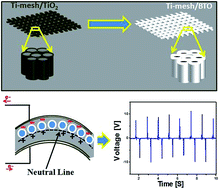
The preparation of a Ti-mesh/BTO was conducted by a straight forward, two step anodization and hydrothermal process, as shown schematically in Fig. 1a. First, well aligned TiO2 nanotube arrays were prepared on a Ti-mesh substrate using an anodization reaction (Fig. 1b(i)). Subsequently, the anodized samples were treated hydrothermally in an alkaline solution containing Ba precursor. After a sufficient hydrothermal time had elapsed, the anodized TiO2 nanotube samples were converted to a BTO perovskite film and attached firmly to the Ti-mesh substrate, as shown in the optical image of Fig. 1b(ii).
image file: c6ra13482c-f1.tif
Fig. 1 (a) Schematic representation for the fabrication process of BTO nanotube arrays on flexible Ti-mesh substrate. (b) Photographic image of TiO2 (i) and BTO (ii) nanotube film on Ti-mesh substrate. (iii) Ti-mesh/BTO bent by finger with dimensions of 2 cm × 2.5 cm.

The morphology of the samples before and after the hydrothermal treatment was examined by SEM. Fig. 2a–c presents the surface and cross-sectional morphology of the prepared TiO2 nanotubes before the hydrothermal treatment. The nanotubes had an approximate length and diameter of ∼7 μm and ∼50 nm, respectively, after an 8 h anodization time. During the transformation process, the TiO2 nanotube samples, which were prepared for an 8 h anodization time, were treated hydrothermally for different times (8, 12, and 24 h) at 210 °C. After heat treatment, the smooth nanotube structure of TiO2 was changed to a similar nanostructured BTO nanotube array following the morphology of the TiO2 nanotube arrays as a template, as shown in Fig. 2d–f. The length of the converted BTO nanotubes remained approximately the same, where as the diameter decreased significantly. The decrease in diameter of the BTO nanotubes was attributed to the volume expansion during the phase change from rutile titanium oxide to cubic/tetragonal BTO (Fig. 2e).


image file: c6ra13482c-f2.tif
Fig. 2 Cross-sectional (a), surface (b) and magnified cross-sectional (c) SEM image of TiO2 nanotube arrays synthesized at 8 h anodization time. Cross-sectional (d) surface (e) and magnified cross-sectional (f) SEM image of BTO nanotube arrays on Ti-mesh substrate, after hydrothermal conversion of the TiO2 nanotube for 24 h (g) EDX analysis of Ti-mesh/BTO prepared at 24 h hydrothermal time.

The formation of BTO occurs due to the dissolution of TiO2 and the subsequent reaction with Ba ions through Ostwald ripening.34,35 The porosity and the spacing between the nanotubes allow the reaction between Ba ions and the dissolution of TiO2 nanotubes during the hydrothermal process. The reaction steps are expressed in chemical eqn (1) and (2).36,37 In the first step, the Ti–O bonds from TiO2 are broken due to hydrothermal attack, which results in the formation of soluble [Ti(OH)6]2−. In the next step, Ba2+ ions react with [Ti(OH)6]2− to produce BTO nuclei in the vicinity of the TiO2 nanotube surface. After a sufficient growth time, the TiO2 nanotube is transformed to a nanostructured BTO nanotube array.

 
TiO2 + 2OH + 2H2O → [Ti(OH)6]2− (1)
 
Ba2+ + [Ti(OH)6]2− → BaTiO3 + H2O (2)

The elemental profile of the converted sample was examined by EDX, as shown in Fig. 2g. The peaks originating from Ti (L-edge) and O (k-edge), as well as the peaks of Ti (k-edge) and Ba (L-edge) appeared and overlapped with each other at 4–5 eV and 0–1 eV, respectively. EDX also revealed the existence of O, Ba, and Ti with a relative concentration of 24.11, 36.94 and 37.23 wt%, respectively.

X-ray diffraction (XRD) is used to examine the formation of BTO perovskite crystals, as shown in Fig. 3a. The XRD patterns of the as-grown anodized TiO2 nanotube prepared at 8 h anodization time revealed peaks originating from the Ti-substrate (Fig. 3a(i)), which are the characteristic peaks for amorphous TiO2 nanotubes.38 Fig. 3a(ii) and (iii) indicate XRD peaks of the BTO film prepared for an 8 and 12 h hydrothermal time, respectively. The majority of the peaks matched the peaks of BTO (JCPDS no. 350757) and peaks observed around 23° and 65° were indexed to the (101) and (204) peaks of TiO2 nanotubes, respectively.38 This clearly indicates the transformation of TiO2 nanotubes to BTO perovskite structure with a trace amount of TiO2. The strong intensity peaks at (001) and (002) of the BTO nanotube film suggests a strong 〈00L〉 orientation of the converted samples. Generally, the tetragonal phase of BTO is piezoelectrically active and is identified by peak splitting around 2θ = 45°.39 As shown in the inset of Fig. 3a, the expected peak splitting was not observed for the samples prepared at an 8 and 12 h hydrothermal growth time. This suggests that the majority of the peaks are due to cubic phase BTO nanotube film. Raman spectroscopy was performed to further investigate the transformed sample and its phase, as shown in Fig. 3b. Three Raman active modes of BTO at 154 [A1(TO1)], 250 [A1(TO2), E(LO)], and 520 cm−1 [A1(TO), E(TO)] were identified for all hydrothermally treated samples. According to the literature, the tetragonal phase of BTO are known by the Raman peaks around 308 [B1, E(TO + LO)] and 720 cm−1 [A1(LO), E(LO)].40 As shown from the Raman spectrum, the samples prepared at 8 and 12 h hydrothermal time show a weak peak at 310 cm−1 and no peak at 720 cm−1. Therefore, from XRD and Raman spectroscopy both the samples prepared at 8 and 12 h hydrothermal reaction time were not in the tetragonal phase. To obtain tetragonal phase BTO was prepared for a longer hydrothermal time.40 Fig. 3a(iv) and b show the XRD pattern and Raman spectrum for the sample prepared for a 24 h hydrothermal time, respectively. The XRD pattern and the inserted magnified view indicate that the peak at 45° shows (002)/(200) splitting. Therefore, both XRD analysis and the Raman peaks at 310 and 725 cm−1 suggest that the sample obtained was in the tetragonal phase. The result also revealed the disappearance of peaks from the TiO2 nanotube for the samples prepared for a 24 h hydrothermal time, indicating the complete conversion of the sample to the BTO nanotube array. The peak at 2θ = 27.5° is the (111) peak of BaCO3 (JCPDS 41-0373), which indicates the existence of trace amount of BaCO3.


image file: c6ra13482c-f3.tif
Fig. 3 (a) XRD patterns of the as-grown TiO2 nanotube (i) and BTO nanotube film for hydrothermal time of 8 (ii), 12 (iii) and 24 h (iv). Inset: XRD peaks at 2θ ∼ 45° indicating peak splitting for the sample prepared at 24 h hydrothermal time. (b) Raman spectrum of the as-grown TiO2 nanotube (Ti–TiO2 NT) and BTO samples for hydrothermal time of 8, 12 and 24 h. Inset: Raman peaks for the sample prepared at 24 h hydrothermal time showing the peaks around 310 and 725 cm−1 indicating tetragonal phase. TEM image of the BTO nanotubes for 12 (c) and 24 h (d) hydrothermal time.

TEM analysis also highlighted the transformation of TiO2 nanotubes to irregularly shaped BTO nanotube arrays, suggesting a phase change due to the hydrothermal treatment (Fig. 3c). This is due the dissolution and recrystallization process occurring around the TiO2 nanotubes wall that affects the starting tubular morphology.40

The grain size of the converted BTO film depends on the size of the TiO2 nanotubes, which itself depends on the anodization time. This was confirmed experimentally by the growing TiO2 nanotubes for different anodization times and hydrothermally converting it to BTO nanotube films. Fig. S2 and S3 present the cross-section SEM images of the individual films, before and after the hydrothermal treatment, respectively. The BTO nanotube film, which was prepared for an 8 h anodization time, was selected to obtain a high grain size and mechanically strong nanotube film, which is crucial for piezoelectric applications.41

3.2 Fabrication and performance of flexible Ti-mesh/BTO-based PENG

Fig. 4a presents a schematic diagram of the PENG device fabrication steps. The oriented tetragonal phase BTO nanotubes arrays grown on the Ti-mesh substrates were used as a piezoelectrically active material for energy generation. Fig. 4b and c present cross-sectional SEM images of Ti-mesh/BTO encapsulated by PDMS, the elastomeric layer. As shown in the schematic diagram, the BTO coated Ti-mesh–PDMS composite was assembled between two ITO-PET electrodes to realize a fully flexible and bendable PENG. The PDMS layer increases the mechanical durability of the PENG device and protects the BTO film from detaching from the Ti-mesh substrate during repeated bending and releasing actions. Fig. 4d presents a photograph of the final PENG device. The image confirms that the device is fully bendable and flexible. Fig. 4e shows the poling process of the Ti-mesh/BTO-based PENG device. During the poling process, a high electric field was applied along the perpendicular direction of the Ti-mesh/BTO; the ferroelectric domains (dipole moments) inside the Ti-mesh/BTO would rotate in the direction of the electric field to enhance the polarization of the composite film.
image file: c6ra13482c-f4.tif
Fig. 4 (a) Schematic illustration for the fabrication procedure for Ti-mesh/BTO-based PENG device. (b) Cross-sectional SEM image of Ti-mesh/BTO encapsulated with PDMS. (C) Magnified SEM image of single Ti-wire coated with BTO and PDMS films. (d) Photographic image of flexible Ti-mesh/BTO-based PENG. (e) Cross-sectional schematic illustration of Ti-mesh/BTO-based PENG showing alignment of the dipoles before and after poling.

3.3 Power generation mechanism

The electrical output and power generation mechanism of the as-poled PENG device due to the bending and releasing motions were examined, as shown in Fig. 5. The structure of PENG was designed by arranging the piezoelectrically active, Ti-mesh/BTO layer unsymmetrically inside the PDMS encapsulating layer (Fig. 5b and S4). This will produce a maximum tensile or compressive strain on the Ti-mesh/BTO layer to enhance the electrical output. A detail theoretical explanation of the relationship between the position of the active layer with strain and stress of the PENG device is given in eqn (5) and (11) in the ESI.
image file: c6ra13482c-f5.tif
Fig. 5 Cross-sectional schematic diagram of Ti-mesh/BTO-based PENG device and its power generation mechanism when the PENG is at (a) original (b), bending and (c) releasing conditions. (d) Measured output voltage (d) and current (e) for Ti-mesh/BTO-based PENG during bending and releasing mode. Inset shows measured output voltage and current for one cycle. (f) Photographic image of LCD screen before plugged into the PENG device (i). Photographic image of Ti-mesh/BTO-based PENG device showing full scale turned on LCD screen, during bending condition (ii) and when the LCD is turned off, during releasing condition (iii).

During operation of the PENG device, the PDMS encapsulated Ti-mesh/BTO composite film undergoes periodic tensile strain and produces a piezoelectric potential across the top and bottom electrodes. As a result, the electrons are forced to flow back and forth in the external circuit following the bending and releasing of the PENG device, as shown in Fig. 5b and c. Fig. 5d and e presents the resulting open circuit voltage and short-circuit current. A maximum output current of 1.1 μA and voltage of 10.6 V were obtained as result of periodic bending and releasing at a frequency of ∼0.7 Hz. The output voltage is obtained at a strain and strain rate of 0.59%, 0.65 s−1, respectively (calculated using eqn (1), ESI). The resulting open circuit voltage by Ti-mesh/BTO-based nanogenerator is higher than other reported flexible lead-free composite-based nanogenerators, as indicated in Table S1. The output signal obtained from the PENG was sufficient to instantly turn on a full screen LCD with the impact from finger tapping (Fig. 5f(ii) and video file). The poling process was conducted to align the dipoles inside the piezoelectric layer in the same direction to enhance the output voltage and current of the PENG device. The electrical output signals from Ti-mesh/BTO-based PENG under external poling voltage range from 5 to 15 kV is shown in Fig. S5. The maximum output voltage and current reached up to 10.6 V and 1.1 μA, respectively when the poling voltage increases from 5 to 15 kV keeping all other parameters constant. Poling voltage above 15 kV created an electric spark across the poling electrodes due to dielectric break down. This suggests that 15 kV is the optimum poling voltages for our piezoelectric nanogenerator device.

The grain size dependence of the Ti-mesh/BTO-based PENG was evaluated by fabricating different grain sized (anodization time) BTO nanotube films at a fixed (24 h) hydrothermal time. As shown in Fig. 6a, the mean voltage and current increased with increasing grain size at a constant strain rate and bending curvature. This was attributed to the increase in the ferroelectric or polarization property of the Ti-mesh/BTO with the grain size or film thickness.41,42 The relationship between bending angle and the output potential was studied for different bending angles, as shown in Fig. 6b. The Ti-mesh/BTO-based PENG showed excellent flexibility and the generated output signal increased as the bending angle decreased at a given strain rate. This is because of the linear dependence of the output potential on magnitude of deformation (strain) of the piezoelectric active layer (eqn (5) and (11) of ESI).14,30


image file: c6ra13482c-f6.tif
Fig. 6 (a) Output voltage and current signals of Ti-mesh/BTO based PENG according to grain size. (b) Generated voltage signals as a function bending angel (70–120°) measured at a constant strain rate. (c) Stable output voltage generation test conducted to assess mechanical durability of the Ti-mesh/BTO based PENG device both with finger bending for 160 cycles (i) and by repeated bending and releasing using linear motor for 700 cycles (ii). (d) Generated voltage and power density for different values of load resistance due to repeated bending and releasing conditions. The inset shows the circuit diagram used.

A polarity switching test was conducted to confirm the origin of the nanogenerators's output signal, as shown in Fig. S6. The switching of the negative and positive output potential peaks following the polarity change confirmed that the output signal comes from piezoelectric property of the BTO arrays not from any other cause. The PENG device without the Ti-mesh/BTO active layer was also prepared under the same fabrication conditions. A very small output voltage (∼0.38 V) was obtained due to the bending and releasing (Fig. S7), confirming that the origin of the output signal is from the piezoelectric property of the Ti-mesh/BTO.

For a PENG to be practically viable, its stability and output power are both indispensable. To check this, we investigated the stability of the PENG output due to bending and releasing condition driven by a human finger (Fig. 6c(i)) and linear motor (Fig. 6c(ii)) oscillating at a frequency of 2 and 1.4 Hz, respectively. The output voltage maintained a constant value of around ∼10 V for up to 700 cycles, confirming the negligible electrical degradation of the PENG device after repeated operation. Additionally, stable voltage is maintained for 4 days for a total of 2800 cycles (Fig. S8). This high stability of the Ti-mesh/BTO-based PENG is attributed to the robust characteristic of the Ti-mesh BTO composite layer.

To examine the performance of the PENG device, the maximum output voltage was recorded when the PENG device was connected to variable resistors. The output power (P) of the PENG, connected to different external load resistors was calculated using eqn (3):

 
image file: c6ra13482c-t1.tif(3)
where R is the load resistance and V is the maximum output voltage measured at different load resistance. Fig. 6d presents the relationship between the output power and external load resistance. According to the result, the maximum power density of the PENG device was ∼1 μW cm−2 at a load resistance of ∼5.2 MΩ operating under repeated bending and releasing conditions at a frequency, strain and strain rate of 0.7 Hz, 0.59% and 0.65 s−1, respectively.

The output power of the Ti-mesh/BTO-based PENG was higher than other previously reported flexible PDMS-based composite nanogenerators fabricated using oriented monolayer43 and nanowire30 BTO nanostructures. The improvement was attributed to the uniform distribution of oriented BTO nanotube arrays inside the PDMS matrix, rendering effective deformation of the piezoelectrically active layer. Moreover, hydrothermal conversion of anodized TiO2 nanotube film provides up to ∼7 μm thick oriented BTO film that enhances the total energy density of the PENG device.

Although the generated output power was still lower than other flexible BTO nanoparticle-based composite nanogenerators,15,22 the obtained electrical output is still feasible. In addition, the strategy of enhancing the piezoelectric output power by manipulating the BTO nanotube film thickness in the preferred orientation is of significance for improving the performance of the BTO-based, piezoelectric energy harvesting devices. Currently, the authors are working on growing oriented BTO nanotube films on flexible Ti-foil to avoid the inherent void region in the mesh structure without a piezoelectric active layer and enhance the total output power density.

To prove the practical applications of the Ti-mesh/BTO-based PENG, the output voltage was rectified using a bridge circuit and used to charge a commercially available capacitor with a maximum capacitance of 10 μF. The Ti-mesh/BTO PENG could charge the capacitor to ∼3 V after 20[thin space (1/6-em)]000 bending and releasing cycles using a linear motor (Fig. S9). This highlights the practicability of Ti-mesh/BTO-based PENG as a constant current source for small electronic devices.

Overall, the Ti-mesh/BTO-based PENG is advantageous in terms of flexibility, lower toxicity, and electrical stability. Moreover, the in situ conversion of 1D TiO2 to an oriented tetragonal phase BTO provides excellent way to make uniformly distributed BTO film with a tunable thickness on a flexible substrate, without the need for a dispersion enhancer and complicated self-assembly process.

4 Conclusion

A uniform BTO nanotube film is synthesized directly on a Ti-mesh substrate using a two-step anodization and subsequent hydrothermal process. The morphological and crystallographic structure of the samples was analyzed, confirming the in situ conversion of anodized Ti-mesh/TiO2 to a similar structured Ti-mesh/BTO. The obtained BTO film was in the tetragonal phase and piezoelectrically active monolayer film. The Ti-mesh/BTO was encapsulated in PDMS and assembled between two ITO coated PET electrodes to form a flexible PENG. The electrical output from the flexible PENG device reached up to 10.6 V and 1.1 μA due to bending and releasing motion. The output power of the PENG device was sufficient to instantaneously light a full scale LCD screen by harvesting energy from the finger bending and releasing action. This study also addresses the dispersion problem of BTO nanoparticles inside the PDMS matrix by the direct utilization of an oriented 1D BTO nanotube film on a transparent Ti-mesh substrate to make a flexible mechanical energy harvester.

Acknowledgements

This work was supported by the National Research Foundation of Korea (NRF) grant funded by the Korea government (MSIP) (No. 2014R1A2A1A11051146).

References

  1. K. I. Park, M. Lee, Y. Liu, S. Moon, G. T. Hwang, G. Zhu, J. E. Kim, S. O. Kim, D. K. Kim, Z. L. Wang and K. J. Lee, Adv. Mater., 2012, 24, 2999–3004 CrossRef CAS PubMed.
  2. X. Chen, S. Y. Xu, N. Yao and Y. Shi, Nano Lett., 2010, 10, 2133–2137 CrossRef CAS PubMed.
  3. S. N. Cha, J. S. Seo, S. M. Kim, H. J. Kim, Y. J. Park, S. W. Kim and J. M. Kim, Adv. Mater., 2010, 22, 4726–47730 CrossRef CAS PubMed.
  4. Z. Li and Z. L. Wang, Adv. Mater., 2011, 23, 84–89 CrossRef CAS PubMed.
  5. R. Yang, Y. Qin, C. Li, G. Zhu and Z. L. Wang, Nano Lett., 2009, 9, 1201–1205 CrossRef CAS PubMed.
  6. S. Xu, Y. Qin, C. Xu, Y. G. Wei, R. S. Yang and Z. L. Wang, Nat. Nanotechnol., 2010, 5, 366–373 CrossRef CAS PubMed.
  7. L. Lin, Y. F. Hu, C. Xu, Y. Zhang, R. Zhang, X. N. Wen and Z. L. Wang, Nano Energy, 2013, 2, 75–81 CrossRef CAS.
  8. Z. Li, G. Zhu, R. Yang, A. C. Wang and Z. L. Wang, Adv. Mater., 2010, 22, 2534–2537 CrossRef CAS PubMed.
  9. M. Zhang, T. Gao, J. Wang, J. Liao, Y. Qiu, Q. Yang, H. Xue, Z. Shi, Y. Zhao, Z. Xiong and L. Chen, Nano Energy, 2015, 13, 298–305 CrossRef CAS.
  10. J. Briscoe and S. Dunn, Nano Energy, 2015, 14, 15–29 CrossRef CAS.
  11. G. Zhu, R. Yang, S. Wang and Z. L. Wang, Nano Lett., 2010, 10, 3151–3155 CrossRef CAS PubMed.
  12. B. Kumar and S. W. Kim, Nano Energy, 2012, 1, 342–355 CrossRef CAS.
  13. J. Kwon, W. Seung, B. K. Sharma, S. W. Kim and J. H. Ahn, Energy Environ. Sci., 2012, 5, 8970–8975 CAS.
  14. C. K. Jeong, I. Kim, K. I. Park, M. H. Oh, H. Paik, G. T. Hwang, K. No, Y. S. Nam and K. J. Lee, ACS Nano, 2013, 7, 11016–11025 CrossRef CAS PubMed.
  15. S. H. Shin, Y. H. Kim, M. H. Lee, J. Y. Jung and J. Nah, ACS Nano, 2014, 8, 2766–2773 CrossRef CAS PubMed.
  16. K.-I. Park, S. Xu, Y. Liu, G.-T. Hwang, S.-J. L. Kang, Z. L. Wang and K. J. Lee, Nano Lett., 2010, 10, 4939–4943 CrossRef CAS PubMed.
  17. M. Wu, C. Xu, Y. Zhang and Z. L. Wang, ACS Nano, 2012, 6, 4335–4340 CrossRef PubMed.
  18. J. Chang, M. Dommer, C. Chang and L. Lin, Nano Energy, 2012, 1, 356–371 CrossRef CAS.
  19. Z. H. Lin, Y. Yang, J. M. Wu, Y. Liu, F. Zhang and Z. L. Wang, Appl. Phys. Lett., 2003, 83, 440–442 CrossRef.
  20. Y. Saito, H. Takao, T. Tani, T. Nonoyama, K. Takatori, T. Homma, T. Nagaya and M. Nakamura, Nature, 2004, 432, 4–87 CrossRef PubMed.
  21. Z.-H. Lin, Y. Yang, J. M. Wu, Y. Liu, F. Zhang and Z. L. Wang, J. Phys. Chem. Lett., 2012, 3, 3599–3604 CrossRef CAS PubMed.
  22. Y. Zhao, Q. Liao, G. Zhang, Z. Zhang, Q. Liang, X. Liao and Y. Zhang, Nano Energy, 2015, 11, 719–727 CrossRef CAS.
  23. K.-I. Park, M. Lee, Y. Liu, S. Moon, G.-T. Hwang, G. Zhu, J. E. Kim, S. O. Kim, D. K. Kim, Z. L. Wang and K. J. Lee, Adv. Mater., 2012, 24, 2999–3004 CrossRef CAS PubMed.
  24. W. Wu, S. Bai, M. Yuan, Y. Qin, Z. L. Wang and T. Jing, ACS Nano, 2012, 6, 6231–6235 CrossRef CAS PubMed.
  25. S. Y. Xu, Y. W. Yeh, G. Poirier, M. C. Mc Alpine, R. A. Register and N. Yao, Nano Lett., 2013, 13, 2393–2398 CrossRef CAS PubMed.
  26. M. Zhang, T. Gao, J. Wang, J. Liao, Y. Qiu, H. Xue, Z. Shi, Z. Xiong and L. Chen, Nano Energy, 2015, 11, 510–517 CrossRef CAS.
  27. Z.-H. Lin, Y. Yang, J. M. Wu, Y. Liu, F. Zhang and Z. L. Wang, J. Phys. Chem. Lett., 2012, 3, 3599–3604 CrossRef CAS PubMed.
  28. Z. Zhou, Y. Lin, H. Tang and H. A. Sodano, Nanotechnology, 2013, 24, 095602 CrossRef PubMed.
  29. S. Moon, H.-W. Lee, C.-H. Choi and D. K. Kim, J. Am. Ceram. Soc., 2012, 95, 2248–2253 CrossRef CAS.
  30. K.-I. Park, S. B. Bae, S. H. Yang, H. I. Lee, K. Lee and S. J. Lee, Nanoscale, 2014, 6, 8962–8968 RSC.
  31. Z. Liu, V. (Ravi) Subramania and M. Misra, J. Phys. Chem. C, 2009, 113, 14028–14033 CAS.
  32. W. He, J. Qiu, F. Zhuge, X. Li, J. H. Lee, Y. D. Kim, H.-K. Kim and Y.-H. Hwang, Nanotechnology, 2012, 23, 225602 CrossRef PubMed.
  33. Z.-J. Zhang, Q.-Y. Zeng, S.-L. Chou, X.-J. Li, H.-J. Li, K. Ozaw, H.-K. Liu and J.-Z. Wang, Electrochim. Acta, 2014, 133, 570–577 CrossRef CAS.
  34. J. O. Eckert Jr, C. C. Hung-Houston, L. Gersten, M. M. Lencka and R. E. Riman, J. Am. Ceram. Soc., 1996, 79, 29–39 CrossRef.
  35. J. Q. Qi, T. Peng, Y. M. Hu, L. Sun, Y. Wang, W. P. Chen, L. T. Li, C. W. Nan and H. L. Chan, Nanoscale Res. Lett., 2011, 6, 466 CrossRef PubMed.
  36. L. Qi, B. I. Lee, P. Badheka, D.-H. Yoon, W. D. Samuels and G. J. Exarhos, J. Eur. Ceram. Soc., 2004, 24, 3553–3557 CrossRef CAS.
  37. Y. Xin, J. Jiang, K. Huo, T. Hu and P. K. Chu, ACS Nano, 2009, 3, 3228–3234 CrossRef CAS PubMed.
  38. J. H. Yang, C. W. Bark, K. H. Kim and H. W. Choi, Materials, 2014, 7, 3522–3532 CrossRef CAS.
  39. P. Sa, J. Barbosa, I. Bdikin, B. Almeida, A. G. Rolo, E. M. Gomes, M. Belsley, A. L. Kholkin and D. Isakov, J. Phys. D: Appl. Phys., 2013, 46, 105304 CrossRef.
  40. A. Lamberti, N. Garino, K. Bejtk, S. Bianco, S. Stassi, A. Chiodoni, G. Canavese, C. F. Pirriab and M. Quaglio, New J. Chem., 2014, 38, 2024–2030 RSC.
  41. Z. Zhao, V. Buscaglia, M. Viviani, M. T. Buscaglia, L. Mitoseriu, A. Testino, M. Nygren, M. Johnsson and P. Nanni, Phys. Rev. B: Condens. Matter Mater. Phys., 2004, 70, 024107 CrossRef.
  42. Y. Hu, Y. Zhang, C. Xu, G. Zhu and Z. L. Wang, Nano Lett., 2010, 10, 5025–5031 CrossRef CAS PubMed.
  43. T. Gao, J. Liao, J. Wang, Y. Qiu, Q. Yang, M. Zhang, Y. Zhao, L. Qin, H. Xue, Z. Xiong, L. Chena and Q.-M. Wang, J. Mater. Chem. A, 2015, 3, 9965–9971 CAS.

Footnote

Electronic supplementary information (ESI) available. See DOI: 10.1039/c6ra13482c

This journal is © The Royal Society of Chemistry 2016