DOI:
10.1039/C6RA13430K
(Paper)
RSC Adv., 2016,
6, 69027-69032
Highly conductive air-stable ZnO thin film formation under in situ UV illumination for an indium-free transparent electrode†
Received
24th May 2016
, Accepted 14th July 2016
First published on 14th July 2016
Abstract
Zinc oxide (ZnO) is considered as the strongest alternative to tin doped indium oxide (ITO) – a commonly used, but an expensive state-of-the-art material for transparent conducting electrodes. This work reports the low temperature atomic layer deposition (ALD) of a highly transparent, and highly conductive air-stable thin film of ZnO under in situ UV irradiation of the growing film. X-ray photoelectron spectroscopy (XPS) reveals that the UV irradiation generates oxygen vacancies, partially removes O–H bonds, and thereby improves the electrical conductivity. Thus, in contrast to 0.25 Ω cm resistivity of the pristine ZnO film, the in situ UV irradiated ZnO film shows an electrical resistivity of 5.5 × 10⁻⁴ Ω cm, and an optical transparency of nearly 90%, which are closer to that of ITO. In addition, even on prolonged exposure of the film to air, it demonstrates high stability against the degradation of the electrical conductivity.
1. Introduction
Materials having high optical transparency and high electrical conductivity have received great attention for designing transparent conducting electrodes, which are widely used in various optoelectronic devices for transparent electronics and sustainable energy generation, such as light-emitting diodes, smart electronic windows, displays, touch screen panels, and solar cells.1–10 To date, the most common materials for transparent conducting electrodes are transparent conductive oxides having a wide band gap to transmit the visible spectrum of light. In particular, tin doped indium oxide (ITO) is considered as a state-of-the-art material for a transparent conducting electrode11 owing to its outstanding conductivity of ∼10−4 Ω cm at a high transparency of 85–90% transmittance for visible light. However, indium being a rare metal, ITO suffers from high cost of production. Moreover, fabrication of ITO film is a high temperature process, and ITO has inherent brittleness, which limits to use ITO freely in flexible electronics. To overcome these limitations, various alternative inexpensive materials, which are abundantly available and could be supplied sustainably are gaining importance.11–17 Among them, transparent conducting ZnO thin films are emerging as the strongest alternative to ITO due to its synthesis form earth abundant metal, biocompatible, and easy to fabricate.11,17,18 However, despite being transparent to visible light, intrinsically pure ZnO exhibits only semiconductor level of electrical conductivity. Basically, the electrical conductivity (σ = neμ) of an oxide film depends mainly on the carrier concentration (n) and carrier mobility (μ).19 Any phenomena that enhance these two key factors can essentially improve the conductivity of the oxide. The intrinsic carrier concentration of ZnO lies in between 1018 to 1019 cm−3, which is not enough to provide satisfactory level of conductivity to be used in transparent conducting electrodes. Therefore, doping of impurities is essential, and this strategy has already become a well-established and indispensable approach to meet the high conductivity requirements. Variety of metal ions, particularly from the group III such as Al, In, Ga, etc. are doped within the ZnO film.11,17–22 These trivalent dopants substitute Zn ions and thereby generate free electrons. As a result, the carrier concentration of the doped ZnO is increased.19 Note that the concentration of the dopants should be critically optimized in order to obtain the utmost optoelectronic properties of the doped film. For example, doping with higher concentration of dopant leads to enhance the carrier concentration, and thereby it enhances the conductivity correspondingly. Meanwhile, it inevitably yields the film with poorer optical transmission. As discussed above, the conductivity of ZnO film can also be enhanced by improving the carrier mobility. It is known that the negatively charged oxygen species at grain boundaries act as trapping centers that suppress electron transfer. Thus, the grain boundary defects decrease carrier mobility. Passivation of grain boundary by thermal treatment of ZnO in reducing atmosphere such as in hydrogen can simply reduce the potential barrier for electron transfer at grain boundaries.19
Apart from the hetero atom doping, a second strategy to enhance carrier concentration by UV irradiation has also been reported.19,23–25 The importance of UV irradiation relies in the strategy to create oxygen vacancies in ZnO lattice in order to enhance the free electron concentration, thereby improving the electrical conductivity of the ZnO film. In fact, the influence of illumination on improvement of conductivity of ZnO was first reported in 1957,26 and this phenomenon has been used in applications of gas sensors and photocatalysis.27–29 Generally, the UV light induced conductivity of ZnO called as “persistent photoconductivity” decays constantly when exposed to air in dark, and retains the original conductivity of the ZnO over a timescale of hours to days. However, recently Vai et al. have demonstrated that the in situ UV irradiation during the deposition of ZnO film by spray pyrolysis can prolong the stability of the UV induced conductivity.30 It should be noted that the ZnO film deposited at 334 °C in their work exhibited the lowest electrical resistivity of 6.13 × 10⁻² Ω cm with the maximum optical transparency of 73.6%. Meanwhile, the resistivity and the optical transparency increased to 117.65 Ω cm and 87%, respectively when they reduced the deposition temperature to 250 °C. The electrical conductivity and the optical transparency of their ZnO films are poor to be used as transparent conductive film. Based on the above fact that the in situ UV irradiation can induce an enhanced conductivity that can last for longer time even when the film is exposed to air, herein we perform the in situ UV irradiation during atomic layer deposition (ALD) of ZnO film at 65 °C. This enabled us to obtain highly transparent and conductive ZnO film without any external aid of doping impurities. Large varieties of methods are available to fabricate transparent conductive ZnO films.11,17,18,22 Despite the high investment costs associated with the instrumental complexity, and the availability of low-cost of non-vacuum based methods, vacuum based routes particularly ALD method is largely employed on industrial scale to grow transparent conductive ZnO thin films. This is due to the fact that the ALD is superior than other vacuum based methods in producing homogeneous and nanocrystalline high quality thin films having high conductivity and transparency, together with the advantage on close control of doping concentration and film thickness in nanometer scale of the method.17 In addition, among the other vacuum based deposition techniques, ALD method is a versatile technique enabling deposition of conformal and uniform films over large-area even on very complex substrates at low temperatures. Therefore, we employed the ALD method in the present work. In contrast to the normal ALD growth of ZnO film, when in situ irradiation of the growing ZnO film was performed with UV light in a typical ALD process as shown in Fig. 1, highly air-stable thin film having transparent and conducting performance similar to the benchmark ITO electrode was achieved.
 |
| | Fig. 1 Schematic diagram of UV-enhanced ZnO film deposition in ALD reactor. | |
2. Experimental
All chemicals were reagent grade, and were used as obtained from the suppliers without further purification. As substrate, borosilicate non-conducting glass as well as chemically cleaned p-type Si(100) were used. To deposit ZnO film, diethylzinc (DEZ, Zn 52 wt% Aldrich) and water were used as zinc and oxygen precursors, respectively. These precursors were vaporized at 20 °C, and delivered with argon as carrier gas to the ALD reactor at the rate of 50 sccm. The detailed ALD sequence is shown in Scheme S1 of the ESI† section. Briefly, each ALD cycle was consisted of 2 s exposure of the substrate to DEZ vapor at 20 mTorr followed by purging out the non-physisorbed DEZ by pure argon gas for 20 s, then 2 s exposure of the substrate to water vapor at 20 mTorr followed by purging out the non-reacted water vapor by pure argon gas for 60 s. The deposition of ZnO films was performed at 65 °C. As illustrated in Fig. 1 and Scheme S1,† in situ UV irradiation to the growing ZnO film was carried out during feeding and purging the water vapor out from the ALD chamber. The UV source was a 1 kW UV lamp (LH-100/100-A, 365 nm UV emission), and the irradiation was performed by illuminating the substrate through the quartz glass window coated with CYTOP polymer at the ALD chamber.
The film thickness was measured using an ellipsometer. Optical transmission of the film was measured using an UV-visible spectrophotometer (Agilent 8453 UV-visible Spectroscopy), and the electrical resistivity of the film was measured using a four-probe measuring device (HP 4155C, Agilent Technologies). Film morphology was investigated using field emission scanning electron microscope (Hitachi, S4800). X-ray photoelectron spectra were recorded on a VG scientific ESCALAB MK II spectrometer using Al kα source operated at 15 kV and 10 mA, and the spectra were calibrated using the C 1s peak (284.6 eV).
3. Results and discussion
The reaction for the formation of ZnO thin films using DEZ and water vapor as zinc and oxygen precursors in ALD process is given below in eqn (i).| | |
Zn(C2H5)2 + H2O → ZnO + 2C2H6
| (i) |
The above surface reactions must be self-terminating and complementary to yield uniform and conformal thin film of ZnO. In order to make the above reaction surface saturated self-limiting, the reaction should be completed at the substrate surface in one ALD cycle. For this, we investigated the growth rate of the ZnO films at various feeding time for DEZ and water at constant temperature of 65 °C. Fig. 2a and b show the growth rate of the ZnO film with respect to the feeding time of DEZ and water, respectively. In both cases, the growth increased sharply up to 1 s, and thereafter it became more gradual. Finally, the growth attended the saturation level, when the feeding time of the precursors reached 2 s. Thus, by manipulating the feeding time of the precursors, self-limiting surface reaction was achieved, which is generally supposed to yield the highly conformal film. In addition, this self-limiting surface reactions afford a great deal of control over the film growth as shown in Fig. 2c, whereby the film with desirable thickness can be obtained. The setup for in situ irradiation of the growing ZnO film with UV light is shown in Fig. 1, which consists of a quartz glass window in a typical ALD setup for UV irradiation facility. As illustrated in Fig. 1, the quartz window is coated with CYTOP polymer film. The role of the CYTOP coat is to prevent the deposition of ZnO on the window, and thereby avoiding the blockage of the UV radiations to be penetrated and reach at the growing ZnO film. Therefore, before studying the influence of UV light irradiation to the growing film, the efficiency of the CYTOP coat for prevention of the ZnO deposition on the ALD quartz glass window was investigated. For this, ALD cycles ware performed to deposit several ZnO films having approximately 160 nm thick, and subsequently the CYTOP coated quartz was investigated using an UV-visible spectrophotometer. Fig. S1a and b† show the optical transmittance spectra of the CYTOP coated quartz before and after the ALD reaction, which exhibited almost the similar transmittance. The small difference of about 5% optical transmission observed at the mean 365 nm wavelength of the UV source in Fig. S1a and b† could be due to the deposition of very small amount of ZnO on the CYTOP surface. This finding confirms the effective penetration of the UV light during ALD process through the quartz window coated with CYTOP.
 |
| | Fig. 2 Dosing time of precursors to achieve self-limiting surface reaction for formation of ZnO. (a) DEZ and (b) H2O. (c) Growth rate of ZnO film as a function of ALD cycle number. | |
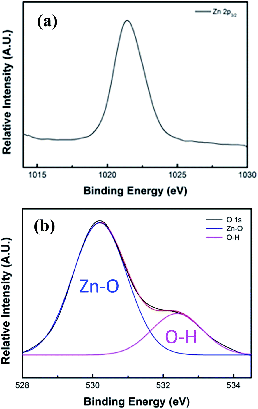
As a transparent electronic material, the primary requirement is that the film should have high electrical conductivity. Fig. 3 shows the variation on the electrical resistivity of the approximately 160 nm thick ZnO film grown on a non-conducting borosilicate glass substrate with respect to the UV irradiation time per ALD cycle. Initially, the film without UV irradiation exhibited the resistivity of about 0.25 Ω cm. However, the resistivity dropped dramatically with the irradiation time up to 4 s, and subsequently the variation of the resistivity became more gradual. Finally, the resistivity remained almost unchanged beyond 42 s of irradiation. Based on this characteristics, the UV irradiation time per ALD cycle was optimized to 62 s (i.e., 2 s during water vapor exposure + 60 s during water vapor purging out), and under this irradiation condition, the ZnO film achieved the resistivity of as low as 5.5 × 10⁻⁴ Ω cm. Note that the resistivity of the film obtained at this condition is closer to the benchmark ITO film. For further characterization of the film, approximately 160 nm thick ZnO films with and without (pristine – ZnO) UV irradiation were deposited on the non-conducting glass substrates. Fig. 4 shows the SEM side view of the pristine – ZnO film, and the film grown with in situ UV irradiation for 62 s per ALD cycle, which reveals the uniform deposition of the ZnO throughout the film. As in generally obtained ALD ZnO film, columnar growth of the ZnO can be observed in both cases. However, the in situ UV irradiated film exhibited rougher surface. A similar work reported previously on deposition of ZnO by the ALD with DEZ/water vapor precursors demonstrated the wurtzite structured crystalline ZnO at low deposition temperatures ranging from room temperature of 23 °C up to 70 °C.31 This suggests that the ZnO films of the current work have wurtzite crystalline structure. In order to understand the influence of UV irradiation on the enhanced electrical conductivity observed in Fig. 3, XPS investigation of the ZnO films was performed. Fig. 5a and b show Zn 2p3/2 and O 1s XPS spectra of the in situ UV irradiated film. The Zn 2p3/2 XPS spectrum has a well-defined peak positioned at the binding energy of 1021.81 eV, which can be assigned to Zn–O bonding. However, the shape of O 1s XPS spectrum suggests that the spectrum should be deconvolated. As has been reported previously, the O 1s peak was deconvolated into 2 splitting peaks.32 The peak at 532.4 eV can be assigned to residual O–H bonding caused by the introduction of O–H− ions from water vapor used as oxygen precursor in the ALD process, while the other peak positioned at the binding energy of 530.20 eV can be assigned to Zn–O bonding. In contrast to the XPS spectra of the pristine ZnO film shown in Fig. S2 (ESI†), slightly binding energy shift towards lower binding energy are observed in the case of in situ UV irradiated film. The binding energy shifts in Zn 2p3/2 and O 1s XPS spectra of the UV irradiated film can be attributed to the generation of oxygen vacancy in the film. By integrating the area under the peaks, the relative quantity of oxygen and zinc was estimated. The detail ratios of O/Zn and O–H/Zn–O in the pristine and UV irradiated ZnO films are tabulated in Table 1. As evident in the Table 1, the O/Zn ratio of the UV irradiated ZnO film is significantly smaller as compared to that of the pristine ZnO film. This implies that the irradiation of UV light can generate large number of oxygen vacancies to ZnO lattice. These oxygen vacancies act as donor in the ZnO film, and thereby increases the electron concentration in the film.33 As a result, the irradiation of UV light to the growing ZnO increased the electrical conductivity as demonstrated in Fig. 3. Vai et al. have suggested that the effects of in situ UV irradiation and the persistent photoconductivity act simultaneously, and thereby determine the level of donor/acceptor density in ZnO film.30 Further, theoretical calculations of Li et al. suggest that oxygen vacancies at ZnO surface lead to the formation of surface donor states.34 Meanwhile, the experimental observations of Gurwitz et al. suggest that a substantive population of surface oxygen vacancies could be formed under the hole-rich conditions of UV irradiation.35 Hence, the enhanced population of surface donors generated by the in situ UV irradiation partially compensate the acceptors, and thereby leads to a higher electrical conductivity. On the other hand, the O–H/Zn–O ratio of the UV irradiated film is comparatively very smaller than the ratio on the pristine ZnO film. The residual O–H bonds located in the intestinal defect sites act as trap, and thereby decrease the carrier mobility, whereas the O–H bonds located in the oxygen vacancy sites decrease the oxygen vacancies, and hence decrease the carrier concentration.32 Thus, these overall mechanisms contribute in enhancing the electrical conductivity of the in situ UV irradiated ZnO film.
 |
| | Fig. 3 Variation on resistivity of the ZnO film deposited on a glass substrate with respect to in situ UV irradiation time during ALD cycles. | |
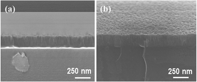 |
| | Fig. 4 SEM side view of ZnO film obtained by ALD method. (a) Pristine ZnO film, and (b) ZnO film under in situ UV irradiation during ALD cycles. | |
 |
| | Fig. 5 (a) Zn 2p3/2 and (b) O 1s XPS spectra of the ZnO film obtained under in situ UV irradiation during ALD cycles. | |
Table 1 Relative ratios of O/Zn and O–H/Zn–O in pristine and in situ UV irradiated ZnO films
| Sample |
Atomic percentage |
O/Zn ratio |
Area under peaks |
O–H/Zn–O ratio |
| O 1s |
Zn 2p3/2 |
Zn–O |
O–H |
| Pristine – ZnO |
42.7 |
57.3 |
0.74 |
66.0 |
34.0 |
0.51 |
| UV – ZnO |
22.4 |
77.6 |
0.29 |
77.2 |
22.8 |
0.29 |
In addition to the high electrical conductivity of the film, optical transparency is another key factor to be considered for the transparent conducting electrode materials. As a transparent electronic material, the film should be transparent enough to transmit visible spectrum of light without any hindrance. Fig. 6 shows the optical transmittance spectra of the above ZnO films deposited on the non-conducting glass substrates. As evident from the spectra, transparency of nearly 90% transmittance for visible and near IR region of light was achieved in all three samples. In line with the transmittance spectrum, the photo image shown in the inset of Fig. 6 also supports the high optical transparency of the UV irradiated ZnO film. In general, extrinsic doping of impurities increases the electrical conductivity of ZnO film up to some level. Meanwhile, it decreases the optical transparency.36 However, in some cases of extrinsic doping, blue-shift in optical gap of ZnO films has also been reported.37,38 Such blue-shift is usually caused by the Burstein–Moss effect.39,40 In any cases, the compromise between the conductivity and the transparency of the ZnO film should be established, and an ideal transparent conducting ZnO film would be the one in which the introduction of defects would have minimum influence on the degradation of optical transparency. The above findings in the current case of in situ UV irradiation suggest that, in contrast to the general case of extrinsic doping, UV irradiation of the growing ZnO films does not have influence on the transparency of the films. Moreover, it should be noted that the degree of transparency of all the films is comparable to that of the ITO film.
 |
| | Fig. 6 Optical transmission spectra of pristine and in situ UV irradiated ZnO film on a glass substrate. | |
Apart from the high electrical conductivity and high optical transparency, stability of the transparent conducting electrode particularly against the degradation on the conductivity is also very important issue. To investigate if the modification on electrical conductivity of the ZnO film caused by the UV light induced oxygen vacancies can be reversed back on prolong exposure of the film to air, the UV irradiated ZnO films were stored for 5 months at room temperature, pressure and humidity in air. The change in electrical resistivity before and after storing the films for 5 months is shown in Fig. 7, which reveals very little change in resistivity. The closer values of resistivity of the fresh and the stored films in air demonstrate the high stability of the films against the degradation on the electrical conductivity. The observed high stability of the films in air is due to the fact that the enhanced population of surface donors generated by the in situ UV irradiation partially compensate for the acceptors that form upon subsequent air exposure, and thereby maintains higher electrical conductivity. Finally, it should be noted that the highly transparent and conductive ZnO film is achieved at very low temperature regime (65 °C), which is a crucial issue for many novel applications such as 3-D nonvolatile memories and for temperature sensitive organic electronics.
 |
| | Fig. 7 Resistivity of the in situ UV irradiated ZnO films on a glass substrate before and after storing for 5 months in air. | |
4. Conclusions
The present work demonstrates that the in situ UV irradiation to the growing ZnO film can significantly enhance the electrical conductivity of the film without degrading the optical transparency. The XPS investigation of the film suggests that the improvement on the electrical conductivity is related to the oxygen vacancies, and partial removal of O–H bonds, which provide the free charge carriers with enhanced mobility for electrical conduction in the oxide layer. More importantly, the prolong exposure of the film to air demonstrated the high stability of the film against the degradation of conductivity. Unlike the general case in extrinsic doping of the ZnO film with various dopants, the deliberate use of in situ UV light to enhance the population of surface donors in ZnO film represents a new strategy that can offer exciting possibilities to tune the selectivity on conductivity with minimal or without compromising the transparency of the film. In this respect, the currently proposed in situ UV irradiation strategy of the low temperature ALD method could be of immense interest and significance for thin film formation of ZnO with highly transparent, conductive, and air-stable characteristics.
Acknowledgements
This work was supported by the Nano Material Technology Development Program (2012M3A7B4034985), and by Creative Materials Discovery Program (2015M3D1A1068061) through the National Research Foundation of Korea (NRF) funded by the Ministry of Science, ICT & Future Planning. This work was also supported by a grant from the National Research Foundation of Korea (NRF), funded by the Korea government (MIST) (No. 2014R1A2A1A10050257).
References
- H. V. Liu, V. Avrutin, N. Izyumskaya, U. Özgür and H. Morkoç, Superlattices Microstruct., 2010, 48, 458 CrossRef CAS.
- X. W. Sun, J. Z. Huang, J. X. Wang and Z. Xu, Nano Lett., 2008, 8, 1219 CrossRef CAS PubMed.
- A. Nadarajah, R. C. Word, J. Meiss and R. Konenkamp, Nano Lett., 2008, 8, 5354 CrossRef PubMed.
- C. G. Granqvist, Sol. Energy Mater. Sol. Cells, 2012, 99, 1 CrossRef CAS.
- A. Stadler, Materials, 2012, 5, 661 CrossRef.
- C. G. Granqvist, Sol. Energy Mater. Sol. Cells, 2007, 91, 1529 CrossRef CAS.
- H. Zeng, X. Xu, Y. Bando, U. K. Gautam, T. Zhai, X. Fang, B. Liu and D. Golberg, Adv. Funct. Mater., 2009, 19, 3165 CrossRef CAS.
- I. Lim, H. T. Bui, N. K. Shrestha, J. K. Lee and S.-H. Han, ACS Appl. Mater. Interfaces, 2016, 8, 8637 CAS.
- J. Muller, B. Rech, J. Springer and M. Vanecek, Sol. Energy, 2004, 77, 917 CrossRef.
- I. Lim, E.-K. Kim, S. A. Patil, D. Y. Ahn, W. Lee, N. K. Shrestha, J. K. Lee, W. K. Seok, C.-G. Cho and S.-H. Han, RSC Adv., 2015, 5, 55321 RSC.
- T. Minami, Semicond. Sci. Technol., 2005, 20, S35 CrossRef CAS.
- P. Liu, T. P. Chen, X. D. Li, Z. Liu, J. I. Wong, Y. Liu and K. C. Leong, ECS Solid State Lett., 2013, 2, Q21 CrossRef CAS.
- D. Lee, H. Lee, Y. Ahn and Y. Lee, Carbon, 2015, 81, 439 CrossRef CAS.
- J. Jang and J. H. Oh, Adv. Funct. Mater., 2005, 15, 494 CrossRef CAS.
- C. Preston, Z. Fang, J. Murray, H. Zhu, J. Dai, J. N. Munday and L. Hu, J. Mater. Chem. C, 2014, 2, 1248 RSC.
- G. Fu, G. Yan, L. Sun, H. Zhang, H. Guo, J. Wang and S. Wang, RSC Adv., 2015, 5, 26383 RSC.
- T. Tynell and M. Karppinen, Semicond. Sci. Technol., 2014, 29, 043001 CrossRef.
- Y. Liu, Y. Li and H. Zeng, J. Nanomater., 2013, 2013, 196521 Search PubMed.
- J. Hong, K. Katsumata and N. Matsushita, Acta Mater., 2016, 103, 844 CrossRef CAS.
- H. Hagendorfer, K. Lienau, S. Nishiwaki, C. M. Fella, L. Kranz, A. R. Uhl, D. Jaeger, L. Luo, C. Gretener, S. Buecheler, Y. E. Romanyuk and A. N. Tiwari, Adv. Mater., 2014, 26, 632 CrossRef CAS PubMed.
- A. R. Babar, P. R. Deshamukh, R. J. Deokate, D. Haranath, C. H. Bhosale and K. Y. Rajpure, J. Phys. D: Appl. Phys., 2008, 41, 135404 CrossRef.
- A. Janotti and C. G. Van de Walle, Rep. Prog. Phys., 2009, 72, 126501 CrossRef.
- J. Gong, Y. Li and Y. Deng, Phys. Chem. Chem. Phys., 2010, 12, 14864 RSC.
- H. Hagendorfer, K. Lienau, S. Nishiwaki, C. M. Fella, L. Kranz, A. R. Uhl, D. Jaeger, L. Luo, C. Gretener, S. Buecheler, Y. E. Romanyuk and A. N. Tiwari, Adv. Mater., 2014, 26, 632 CrossRef CAS PubMed.
- H. Wagata, N. Ohashi, K. Katsumata, H. Segawa, Y. Wada, H. Yoshikawa, S. Ueda, K. Okada and N. Matsushita, J. Mater. Chem., 2012, 22, 20706 RSC.
- D. A. Melnick, J. Chem. Phys., 1957, 26, 1136 CrossRef CAS.
- R. Martins, E. Fortunato, P. Nunes, I. Ferreira, A. Marques, M. Bender, N. Katsarakis, V. Cimalla and G. Kiriakidis, J. Appl. Phys., 2004, 96, 1398 CrossRef CAS.
- G. Gonçalves, A. Pimentel, E. Fortunato, R. Martins, E. L. Queiroz, R. F. Bianchi and R. M. Faria, J. Non-Cryst. Solids, 2006, 352, 1444 CrossRef.
- J. Gong, Y. Li, X. Chai, Z. Hu and Y. Deng, J. Phys. Chem. C, 2010, 114, 1293 CAS.
- A. T. Vai, V. L. Kuznetsov, J. R. Dilworth and P. P. Edwards, J. Mater. Chem. C, 2014, 2, 9643 RSC.
- J. Malm, E. Sahramo, J. Perälä, T. Sajavaara and M. Karppinen, Thin Solid Films, 2011, 519, 5319 CrossRef CAS.
- S. Kwon, S. Ban, S. Lee, S. Jeon, W. Jeong, H. Kim, S. C. Gong, H. J. Chang, H.-H. Park and H. Jeon, Semicond. Sci. Technol., 2009, 24, 035015 CrossRef.
- P. Liu, T. P. Chen, X. D. Li, Z. Liu, J. I. Wong, Y. Liu and K. C. Leong, ECS Solid State Lett., 2013, 2, Q21 CrossRef CAS.
- H. Li, L. K. Schirra, J. Shim, H. Cheun, B. Kippelen, O. L. A. Monti and J.-L. Bredas, Chem. Mater., 2012, 24, 3044 CrossRef CAS.
- R. Gurwitz, R. Cohen and I. Shalish, J. Appl. Phys., 2014, 115, 033701 CrossRef.
- P. M. Ratheesh Kumar, C. S. Kartha, K. P. Vijayakumar, T. Abe, Y. Kashiwaba, F. Singh and D. K. Avasthi, Semicond. Sci. Technol., 2005, 20, 120 CrossRef.
- V. Bhosle, A. Tiwari and J. Narayan, J. Appl. Phys., 2006, 100, 033713 CrossRef.
- R. K. Shukla, A. Srivastava, A. Srivastava and K. C. Dubey, J. Cryst. Growth, 2006, 294, 427 CrossRef CAS.
- E. Burstein, Phys. Rev., 1954, 93, 632 CrossRef CAS.
- T. S. Moss, Proc. Phys. Soc., London, Sect. B, 1954, 67, 775 CrossRef.
Footnotes |
| † Electronic supplementary information (ESI) available. See DOI: 10.1039/c6ra13430k |
| ‡ These authors contributed equally to this work. |
|
| This journal is © The Royal Society of Chemistry 2016 |
Click here to see how this site uses Cookies. View our privacy policy here.