
 Open Access Article
 This Open Access Article is licensed under a Creative Commons Attribution-Non Commercial 3.0 Unported Licence
Spectroscopic ellipsometry for compositionally induced bandgap tuning of combinatorial niobium–tantalum anodic oxides†
Wolfgang
Limberger
a,
Cezarina Cela
Mardare
ab,
Christoph
Cobet
c,
Juan
Zuo
de,
Achim Walter
Hassel
ab and
Andrei Ionut
Mardare
*a
aInstitute for Chemical Technology of Inorganic Materials, Johannes Kepler University Linz, Altenberger Str. 69, 4040 Linz, Austria. E-mail: andrei.mardare@jku.at
bChristian Doppler Laboratory for Combinatorial Oxide Chemistry, Institute for Chemical Technology of Inorganic Materials, Johannes Kepler University Linz, Altenberger Str. 69, 4040 Linz, Austria
cCenter of Surface and Nanoanalytics (ZONA), Johannes Kepler University Linz, Altenberger Str. 69, 4040 Linz, Austria
dInstitute of Advanced Energy Materials, School of Materials Science and Engineering, Xiamen University of Technology, 600 Ligong Road, Jimei District, Xiamen 361024, Fujian, China
eKey Laboratory of Functional Materials and Applications of Fujian Province, 600 Ligong Road, Jimei District, Xiamen 361024, Fujian, China
First published on 8th August 2016
Abstract
Variable angle spectroscopic ellipsometry (VASE) was used for optical property mapping of anodic oxides grown on a wide spread Nb–Ta thin film combinatorial library (Nb content ranging between 8 and 84 at%) with 2 at% resolution. The microstructure of the parent metal alloys was tuned by modifying the library deposition conditions in order to avoid compositionally induced microstructure dissimilarities between the alloys. This allowed an interpretation of the mixed oxides properties based on a single Tauc–Lorentz oscillator for data fitting. Upon anodization up to 10 V vs. SHE, VASE was used to fit the oxide thickness in order to map the oxide formation factors with the results showing a good agreement with the electrochemical data. The measured bandgap values of the Nb–Ta oxides show a deviation from the linear model based on mixing individual Nb and Ta electronegativities proportional to their atomic fractions. This behavior was explained via an in-depth compositional gradient in the oxides. Minority species are depleted at the metal/oxide interface triggering a non-linear shift in the resulting alloy electronegativity. The Nb–Ta mixed oxides bandgap tuning via compositional tuning of the parent metal has been demonstrated and absorption close to the edge of the visible spectrum was identified above 30 at% Nb.
1. Introduction
The continuous search for oxides with improved properties has reached various fields in materials science, chemistry and physics. A special attention has been lately given to Nb and Ta oxides due to their promising capabilities of nanocomposite formation enhancing photocatalytic activities in electrochemical energy production and/or storage applications including highly relevant modern research topics such as CO2 reduction or water splitting.1–4 A vast range of techniques used for oxide formation is available each having advantages and disadvantages depending on the final desired property. Ellipsometry represents a useful and convenient approach for characterizing the optical properties of Nb2O5 and Ta2O5. Such studies confirm that the refractive index and bandgap of Nb2O5 may increase if the annealing temperature reaches 500 °C while good stability of their optical properties was demonstrated below 300 and 400 °C for Nb2O5 and Ta2O5, respectively.5,6 In the case of Nb2O5, the electrochromic properties were demonstrated for both amorphous and crystalline films due to the splitting of Nb–O or Nb3–O stretching modes.7 Even though thin amorphous Nb and Ta oxide films can be obtained (e.g. using sputtering), electrochemical formation of Nb2O5 and Ta2O5via anodization of the parent metals is regularly the choice when thin and dense oxides with high dielectric constants and breakdown fields are required.8–10 Mixing Nb and Ta in their oxidized form during anodization results in extremely interesting behaviors under UV irradiation.11 Anodic oxides on most valve metals (e.g. Nb and Ta) are amorphous and their crystallization may affect their final properties. Field crystallization of Nb–Ta mixed anodic oxides revealed an almost linear dependence between the alloy composition and oxide properties, i.e. oxide formation factor, density and permittivity.12In the present study a Nb–Ta thin film combinatorial library was deposited using co-sputtering. After a complete crystallographic and microstructural analysis of the metallic alloys obtained, the library was step-wise anodized at various potentials and the resulting oxide libraries were investigated. Variable angle spectroscopic ellipsometry was used for mapping the optical properties of the oxides as a function of their parent metal composition. Additionally, the oxide thickness influence on their final optical properties is discussed.
2. Experimental details
2.1 Thin film Nb–Ta library deposition
In order to investigate the optical properties of mixed Nb–Ta anodic oxides, a thin film parent metal compositional spread was deposited using a co-sputtering system (Mantis Deposition Ltd) with a base pressure of 10−10 hPa and 130 mm deposition distance. Two opposite DC powered sputtering guns (50 mm in diameter) hosting high purity Nb (99.95%, MaTeck Material-Technologie & Kristalle GmbH) and Ta (99.95%, ITL-Vacuum-Components) targets were concomitantly operated at room temperature for this purpose in 5 × 10⁻³ hPa Ar. Borosilicate glass slides (26 × 76 mm2) were used as substrates for the deposition of the Nb–Ta library. During film formation the substrates were not rotated. Prior to each deposition, the substrates were ultrasonically cleaned using acetone, iso-propanol and deionized water followed by high purity nitrogen drying. Three separate substrate batches were used for representing the overall Nb–Ta combinatorial library. The varying composition of each sample within one batch was tuned by modifying the power of each sputtering gun for obtaining a wide spread Nb–Ta thin film library. A self-developed software based on a mixed matter theory model was used to calculate the necessary powers for each sputtering gun. The three Nb–Ta samples were intentionally prepared with a partial overlap in the compositional gradient. The deposition rates of Nb and Ta (calculated from the thickness measured using contact profilometry) were 2.268 nm W−1 h−1 and 2.664 nm W−1 h−1, respectively. The values of the DC powers used for Nb and Ta during the library deposition were 33, 67, 80 W and 84, 56, 22 W, respectively. The thickness of the obtained Nb–Ta films was approximately 300 nm. Pure Nb and Ta thin films were additionally deposited on identical substrates to serve as reference samples.2.2 Anodic oxide formation on Nb–Ta library
Anodic oxide layers were electrochemically grown along the entire Nb–Ta compositional spread. The library was stepwise anodized to allow for the determination of the oxide properties at different thicknesses. All single metal and alloy films were anodized in a pH 6.0 CH3COOH/CH3COONa buffer solution in an electrochemical cell designed to allow for controlled sample dipping before applying the anodizing potential. The anodizations were carried out at potentials ranging between 1 and 10 V vs. standard hydrogen electrode (SHE) using a 1287 Solartron electrochemical interface in a three-electrode configuration. For this purpose a Hg/Hg2(CH3COO)2 μ-reference electrode was fabricated (as described elsewhere) while a Pt mesh was used as the counter electrode.13,14 Starting from 0 V vs. SHE, potentiodynamic anodizations with a potential increase rate of 100 mV s−1 were followed by 200 s potentiostatic polarizations at the maximum achieved potential. An additional potentiostatic anodization step was applied as an electrochemical oxide healing process to ensure complete oxide growth. Each sample was dipped in the electrolyte in a stepwise manner (approximately 4 mm each step) in the direction perpendicular to the compositional gradient to allowing for anodic oxide formation along the entire Nb–Ta library during each step. An anodization potential of 10 V vs. SHE was applied during the first dip step followed by a 1 V potential decrease at each subsequent step. In this way, along the entire Nb–Ta thin film library sufficiently wide anodic oxide stripes with different thicknesses were formed. Exemplifying images of the setup used and of the resulting anodized stripes are presented as ESI.† Two identical samples from each batch were used in order to obtain oxide stripes with thickness corresponding to 10 different anodic potentials between 1 and 10 V (SHE).2.3 Metallic and oxide thin films characterization
The microstructure of the Nb–Ta metallic thin film alloys was investigated prior to anodization using a field emission Zeiss Gemini 1540 XB SEM with 20 kV acceleration voltage and in-lens detection. Compositional mapping of each deposited sample was performed using an EDX analyzer integrated in the SEM system (INCA X-sight, Oxford Instruments). A careful calibration of the EDX-detector was performed prior to each series of measurements using a high purity Co standard (Micro-Analysis Consultants, United Kingdom) and the obtained data were processed using INCA-software. Crystallographic analysis of the Nb–Ta thin film combinatorial library was performed using grazing incidence X-ray diffraction (GIXRD) with a Cu-Kα source (PANalytical X'pert Pro). To minimize the substrate influence, the optimized incident angles ranged between 1.1 and 1.9°.After anodization of the Nb–Ta compositional spread, variable angle spectroscopic ellipsometric (VASE) measurements were carried out on a J. A. Woollam M-2000 DI ellipsometer equipped with a deuterium lamp, a quartz tungsten halogen lamp, a rotating compensator and two spectrographs, which allow for the simultaneous measurement of 700 wavelengths with photon energies ranging between 0.75 and 6.5 eV. Measurements were carried out along the entire anodized Nb–Ta thin film library with a compositional resolution of 2 at% for the various oxide thicknesses. In order to obtain the complex dielectric function of the studied oxide films, a simple two-layer model consisting of an oxide layer on top of a metal substrate was applied. As the metal alloys and the pure metals were 300 nm thick they can be assumed as non-transparent. Therefore, the metal films underneath the oxides were considered as substrates in the model and the borosilicate glass underneath was neglected. For the pure metals, a Kramers–Kronig consistent general B-spline layer represented the metal substrates in the model while the pure oxide film dielectric functions were described by a single Tauc–Lorentz (TL) oscillator, which has been proven suitable for modeling amorphous semiconducting and dielectric materials.15,16 The accuracy of the model was successfully tested for both pure metals and their oxides. In the case of the Nb–Ta alloys, the parent metal was modeled by a Bruggeman effective medium approximation (EMA) using the B-spline fit data of the pure metals, which were linearly mixed according to the compositional information obtained from the EDX analysis. This approximation was necessary due to the valve metal character of Nb–Ta alloys, which passivate in air rendering the pure metal surface experimentally inaccessible. The mixed oxide layers were also approximated using a single TL oscillator. This oscillator model calculates the imaginary part of the dielectric function being dependent on the photon energy E as shown in eqn (1).
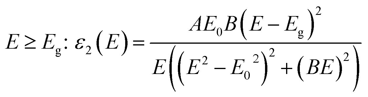 | (1) |
| E < Eg: ε2(E) = 0 |
The factor A in eqn (1) describes the amplitude of the function, E0 represents the peak transition energy, B accounts for the peak broadening while Eg is the band gap energy. Subsequently, ε1 is Kramers–Kronig consistently calculated by integrating ε2:
 | (2) |
3. Results and discussion
The composition of the Nb–Ta thin film combinatorial library was mapped by EDX immediately after the sample deposition. This is a necessary step preceding further properties mappings since it provides the spatial distribution of various alloys along the compositional spread. In Fig. 1 the EDX mapping of the investigated library is presented. The three samples forming the library are separated in the figure by vertical dashed lines and the horizontal axis describes the total cumulative length. The composition of each sample varies approximately linearly with the distance suggesting a weak effect of the cosine law (governing the film thickness spatial distribution) on the composition. This is mainly due to the sputtering geometry used during thin film deposition. Two regions of overlapping composition of at least 5 at% can be observed at the sample boundaries marked in Fig. 1. These regions were further used for checking the continuity of the properties. The composition of the Nb–Ta thin film combinatorial library ranged between Nb–92 at% Ta and Nb–16 at% Ta resulting in a compositional resolution of 0.3 at% mm−1. This wide range spread of Nb–Ta alloys allows further investigations (e.g. XRD, ellipsometry, etc.) with good spatial/compositional resolution. | ||
| Fig. 1 EDX compositional mapping of the Nb–Ta thin film combinatorial library. | ||
The microstructure of the Nb–Ta thin film combinatorial library was investigated using SEM, previous to anodic oxides growth and their optical characterization, in order to observe compositionally induced changes. In previous work, a similar library was characterized and significant changes were observed depending on the Nb–Ta alloy composition.17 The declared aim to investigate the dielectric properties of the anodic oxides grown on the Nb–Ta parent metal alloys by ellipsometry requires a surface as smooth as possible. Surface roughness increases the complexity of the required optical layer model by the need of additional surface layers and can induce depolarization effects, which are difficult to model. Moreover, since the maximum anodization potential used in this study was only 10 V vs. SHE, the anodic oxide is not expected to decrease the overall roughness due to the Nb and Ta oxide formation factors being below 3 nm V−1.10,18 In an attempt to minimize the roughness variation of the Nb–Ta parent metal alloys, the deposition rates of both elements were drastically decreased when compared to the previous study while the Nb and Ta sources were now placed at 180°.
In Fig. 2 a table of selected SEM images is presented describing the current library under study. The surfaces of pure Nb and Ta films produced under similar conditions are shown as references. The amount of Nb in at% is given in each image (pure Ta is indicated by 0 at%). Additionally, the microstructure of the areas with overlapping Nb–Ta composition at the edges of the three samples (30 and 60 at% Nb) is presented. The decrease in the deposition rates did not affect the microstructure of the pure metallic thin films, both Nb and Ta showing grains approximately 30 nm in diameter. If the Nb surface shows one type of surface grain, on Ta two types may be identified. Apart from the round grains forming most of the Ta surface, characteristic pyramidal grains can also be observed. The addition of small amounts of Nb led to surface changes similar to those previously reported.17 An initially smoother surface may be observed for 10 at% of Nb. Increasing the Nb content resulted in less pronounced microstructural changes along the entire Nb–Ta library. One exception can be observed at the first overlapping region between the first two samples (30 at% Nb). Using 33 W for Nb during the library deposition (top row of Fig. 2) resulted in the formation of elongated grain clusters at 30 at% Nb (as suggested by the joined grain boundaries), which did not form when using 67 W during the deposition of the second sample (middle row of Fig. 2). The reason for this is likely related to the individual power densities used in both cases directly influencing the thin film formation. Moreover, the edges of each sample typically suffer from microstructural changes induced by the decreased deposition distance, which locally affects the Nb/Ta atomic ratio. At higher Nb contents, an uneventful transition between the second and third sample was observed (see Fig. 2, middle and bottom row, respectively). In this case 60 at% Nb produced no observable differences between the microstructures visualized on both samples. At the highest Nb concentration, the microstructure of the Nb–Ta thin film resembles the surface of the pure Nb films. Overall, the SEM mapping presented in Fig. 2 reveals very similar surface features along the compositional spread (especially above 30 at% Nb) suggesting that the current Nb–Ta library was suitable for further ellipsometric investigations. For all the analyzed compositions, the grain size average was between 30 and 50 nm, which supports the initial idea of the anodic oxide replicating the parent metal roughness. The previously reported grain elongations and domain formation were successfully avoided here by decreasing the individual deposition rates and maximizing the energy loss per atom.17 This is due to the chosen geometry, which allows for a head-on collision between the Nb and Ta species.
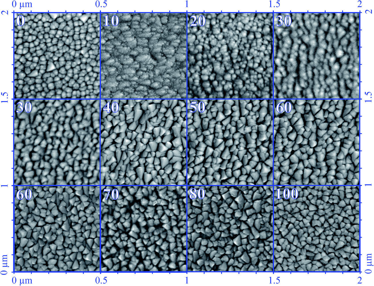 | ||
| Fig. 2 SEM surface microstructure mapping of Nb–Ta thin film compositional spread. The amount of Nb is given in each image in at%. | ||
The crystallography of the Nb–Ta thin film compositional spread under study was characterized using GIXRD at various positions along the library. In Fig. 3 are presented selected diffractograms corresponding to the alloys and reference Nb and Ta films previously imaged in Fig. 2. Pure Nb films are cubic while pure Ta films show tetragonal symmetry. The crystallographic evolution along the Nb–Ta thin film combinatorial library was in agreement with those previously reported.17 Increasing the amount of Nb in Ta resulted in a tetragonal symmetry of the alloys for compositions containing less than 40 at% Nb. Additionally, the presence of a minority cubic phase may be argued here due to the position of the cubic (220) peak, which was shifted by at least 1° when compared to the tetragonal (404) peak. The strong overlapping of the cubic (211) and tetragonal (513) peaks does not help in solving the issue. However, the complete lack of a (513) peak in the diffractogram of tetragonal Ta thin film may indicate that amounts of Nb as small as 10 at% are enough for triggering a minority cubic phase. This was not observed before and may be a direct result of the decrease in the deposition rate. At higher Nb concentrations the alloys are stabilized in the cubic phase. This is clearly observable in Fig. 3, where at low Nb contents the tetragonal phase is mainly identified by the presence of the (002) and (413) peaks. The tetragonal multi-peak centered approximately at 38.5° unfortunately coincides with the cubic (110) peak. Analysis of this peak alone may not be conclusive, but its shape clearly suggests tetragonal peaks overlapping below 30 at% Nb while the full transition to the cubic phase resulted in a much sharper peak. Moreover, the presence of the cubic (310) peak (together with a weak (200) peak) above the mentioned compositional threshold reinforces this conclusion in spite of its coincidence with the tetragonal (513) peak. Tuning the microstructure of the Nb–Ta thin films in the present study did not significantly affect the expected compositionally induced behavior of individual alloys crystalline properties.
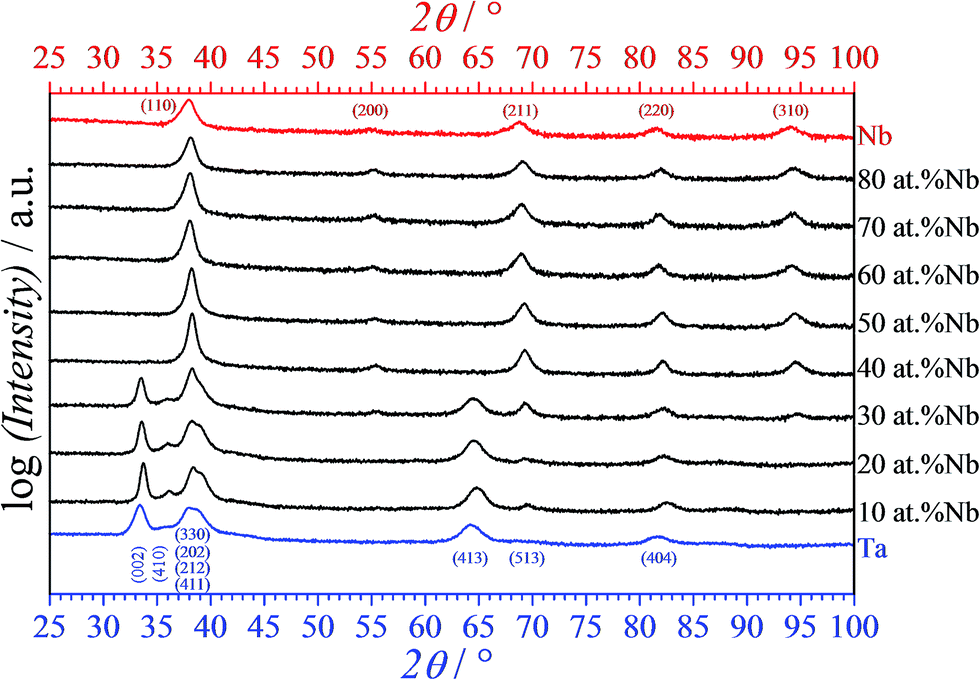 | ||
| Fig. 3 Selected X-ray diffractograms measured in grazing incidence geometry along the Nb–Ta compositional spread. | ||
Anodic oxides were grown along the entire Nb–Ta thin film combinatorial library at once by sequentially dipping the samples in the electrolyte while applying anodic potentials up to 10 V vs. SHE. For this purpose potentiodynamic followed by potentiostatic regimes were used. In Fig. 4 a typical series of cyclic voltammograms (CV) is presented as measured for the middle range sample of the Nb–Ta compositional spread. A clear valve metal behavior was shown by the presence of the oxidation current plateaus, which are visible during the potential increase up to each maximum value. The behavior of the CVs with increasing potential is indicated in Fig. 4 by an arrow pointing in the direction of the highest maximum potential. Moreover, the presence of a current overshoot at the beginning of each anodization step is characteristic to valve metals describing the ion hopping and space charge formation before new oxide is formed.18 For such curves usually the current density is plotted against potential. In the present study this was not possible due to the uncontrolled electrocapillarity effects related to the dipping of the samples in electrolyte during oxide formation. The precise value of the wetted area at each dipping step was difficult to measure precisely. Its increase with the anodization potential was clearly demonstrated by the increase in the oxidation current plateaus with the maximum applied potential. However, an electrochemical interpretation of the CVs with the purpose of mapping the oxide formation factors was inappropriate here (and has been carried out before) since the entire compositional spread was anodized at once. The declared aim of the present study was to controllably grow anodic oxides for further ellipsometric investigations. For this purpose a precise potential control was sufficient. In order to ensure that no ionic species remained trapped in the oxide, a potentiostatic anodization step was applied after each CV. In the inset of Fig. 4, a typical curve is presented. A clear exponential decay (fitted line) of the current with time indicates the charge removal combined with growth of small additional oxides.
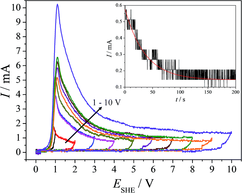 | ||
| Fig. 4 A typical series of cyclic voltammograms (with a step-wise increase in the maximum potential) as measured at the middle range of the Nb–Ta compositional spread. Inlet: the typical potentiostatic anodization performed at the end of each voltammogram. | ||
The anodized Nb–Ta combinatorial library was investigated using VASE in order to characterize the optical properties of the various Nb–Ta oxides. For this purpose, the optical data as sequentially measured for different oxide thicknesses formed up to 10 V (SHE) were simultaneously evaluated. In addition, the thickness of the anodic oxides was obtained using the layer model described in the Experimental section. The imaginary part of the dielectric function (ε2) describing the electronic excitations in the Nb–Ta oxides (i.e. absorption process) was approximated by fitting the VASE data with a single TL oscillator dispersion. A compositional mapping of the TL absorption is presented in Fig. 5 for selected oxide alloys together with the data obtained from anodic oxides grown on the pure metals. Below 2.8 eV all the oxide films along the entire compositional spread are transparent. The oxides grown on alloys containing more than 30 at% Nb possess an absorption onset (Eg) around 3 eV (410 nm; close to the UV limit of the visible spectrum), which shifts for lower Nb concentrations further into the UV region. Above 4 eV (below 300 nm) light absorption can be observed for all analyzed oxides. The absorption maximum of the TL resonance was also shifted to higher photon energies upon increasing the Ta concentration. Both the absorption onset as well as the general line shape (broadening) of the TL resonance changed significantly in the range of 30 to 40 at% Nb. This interesting aspect may be related to the full cubic phase stabilization of the Nb–Ta thin film alloys. Even though, the formed anodic oxides are expected to be amorphous their behavior is dictated by the properties of their parent metals, which directly affect the anodization process.19,20 The mappings of the imaginary part of the dielectric function present peaks located immediately below 30 at% Nb observable at high energies/low wavelengths. This can be related to the transition between the first and second sample as discussed in the SEM analysis (see Fig. 2). The microstructural differences observed in the region of the compositional overlap between these samples contribute only small variations to the measured dielectric properties. However, the distinct trend in the optical properties of the anodized Nb–Ta compositional spread clearly relates to changes in the composition and crystal structure of the parent metal alloy.
 | ||
| Fig. 5 The imaginary part of the dielectric function presented for selected compositions as measured along the anodized Nb–Ta library. | ||
Correlating the optically determined thicknesses of the oxide films with the known anodization potentials allows a direct calculation of the oxide formation factors. In Fig. 6 the compositional mapping of the oxide formation factor is presented for the entire Nb–Ta thin film combinatorial library. Similar to previous cases, the measurements obtained for the pure oxides were added as references. Additionally, experimental points describing the overlapping compositional regions were added and measurements from each investigated sample are color and shape coded. The optically determined oxide formation factors show a compositional behavior similar to the one electrochemically measured in previous investigations.17 However, small discrepancies between the optical and electrochemical data may be expected due to the different natures of both methods. Above 35 at% Nb the current data matches extremely well the oxide formation factors measured electrochemically (not shown here), which indicates the viability of the spectroscopic ellipsometry approach. Values ranging between approximately 1.8 and 2.6 nm V−1 were calculated from the VASE data. An exception was found when analyzing the compositional range below 30 at% Nb where the optical data indicate a decrease in the oxide formation factor with increasing Nb content. This may be triggered by the microstructure tuning present in the current study as shown and discussed in Fig. 2. Additionally, the transition between the first and second sample of the Nb–Ta library resulted in a discontinuity of the oxide formation factors observable between 25 and 35 at% Nb where the experimental data measured on identical compositions have different values. This may be related to the different parent metal microstructures induced by edge effects as observed during the SEM analysis (see Fig. 2). If the optically determined oxide formation factor of pure Ta oxide matches well with the literature values, the pure Nb oxide formation factor was slightly smaller.18
 | ||
| Fig. 6 Compositional mappings of the oxide formation factors as measured by VASE along the anodized Nb–Ta library. | ||
One of the main goals of VASE was the determination of the optical bandgap of materials. Similar to previous mappings, information was obtained by fitting together all optical data corresponding to oxide thicknesses up to 10 V (SHE). This approach was a compromise necessary in order to reduce the fitting errors as much as possible. For exemplifying this aspect, part (a) of Fig. 7 shows first the compositional mappings of the optical bandgap as fitted for extreme cases using only thin oxides (2 to 4 V) or only thick ones (8 to 10 V). As expected, larger fitting errors were observable for the thin oxides (mainly due to the substrate approximation) while the thick ones resulted in more stabile fitted values. The experimental points in Fig. 7(a) were fitted using multi-peak Lorentzian functions for a simple visualization of the trends of the compositionally induced bandgap variations. For low Nb contents below 30 at% where the cubic phase was not yet stable, both fitted curves indicate an almost identical behavior. However, for higher Nb amounts the bandgaps of thin and thick anodic oxides show differences of up to 0.4 eV as observed at 60 at% Nb. This may suggest that the composition of the mixed anodic oxides changes with the thickness (for a given Nb/Ta ratio) in spite of the cubic phase stabilization of the parent metal alloys. The latter in-depth compositional changes also explain the strong broadening in the TL absorption shown in Fig. 5 where thin and thick oxide films were simultaneously evaluated.
 | ||
| Fig. 7 Nb–Ta anodic oxides optical bandgap mappings for extreme cases of thin and thick oxides (a) and bandgap mapping obtained by fitting the optical dataset for all thicknesses (b). | ||
The optical bandgaps of the anodic oxides grown along the Nb–Ta thin film library obtained by fitting all available optical data (compare Fig. 5) are plotted in Fig. 7(b). The bandgap values measured on the anodized pure Nb and Ta films are also presented. Experimental data obtained from each sample are color and shape coded, and the compositionally overlapping regions are visible. The bandgaps measured for the oxides grown on low Nb content alloys had smaller values when compared with the pure Ta oxide. This decrease by approximately 0.2 eV remains almost constant up to 30 at% Nb. At this compositional threshold the anodic oxide bandgap decreases dramatically reaching values below 3 eV. Even though a discontinuity can still be observed between the first and second sample, the bandgap values indicate clearly a decaying trend upon increasing the Nb content up to 40 at%. Further increasing the Nb concentration in the parent metal alloys did not produce any substantial change with the bandgap having values scattered around 2.9 eV until about 80 at% Nb. At the Nb-rich side of the thin film library, the anodic oxides show an increase in the bandgap values towards the pure Nb oxide value slightly above 3.2 eV. The entire bandgap behavior along the Nb–Ta compositional spread reveals the bandgap tuning possibilities by choosing the right Nb–Ta mixture. Such tuning capabilities were addressed in previous investigations regarding discreet Nb–Ta alloys when a linear dependence between the bandgaps and Nb content was found.11 This is not the case in the present study in spite of the expectations based on the mixed matter theory. Several detailed studies indicate that for amorphous d-metal oxides an empirical equation may be applied:21,22
| Eg − Eam = 1.35(χM − χO)2 − 1.49 | (3) |
In an attempt to correlate the current findings with previously reported results indicating a linear anodic oxide bandgap tuning, from eqn (3) the χM was calculated using the current bandgap values measured by ellipsometry (and plotted in Fig. 7(b)). Since the previously determined value of Eam for Nb–Ta alloys was carried out using a much thinner anodic oxide film, this lattice distortion induced bandgap perturbation will also be considered here. The Eam value obtained for the Nb–Ta alloys was correctly determined before since the mixed matter theory perfectly fitted the experimental findings possibly due to the thinner oxides triggering less pronounced/observable in-depth compositional gradients.11 In Fig. 8 the results are plotted against the composition for the entire analyzed Nb–Ta compositional spread. In addition, the theoretical values of χM calculated using mixed matter theory are also plotted. For this purpose it was considered χNb = 1.60 and χTa = 1.50, both with an absolute error in the range of 0.05 as accepted by Pauling.28 If at Nb contents below the cubic threshold of 30 at% Nb both curves are somehow correlating, above this composition the value of the parent metal electronegativity was much higher than the theoretical value, but still remain in the approximate error range of the Nb value. This difference may be related to the compositional deviation of the anodic oxide when compared to its metallic parent alloy. Literature values are plotted in Fig. 8 describing the behavior of both Nb and Ta in the oxidized state as a function of the parent metal alloy.17 The right side vertical scale in % describes this relative deviation. Below 30 at% Nb a surface enrichment of Nb of up to 40% (together with a depletion of Ta) was detected in the anodic oxides. At higher Nb concentrations this situation changes when a surface depletion of Nb (with a complementary Ta enrichment) was observed. A surface enrichment with one species could imply a depletion of that species at the oxide/metal interface for any given Nb/Ta cationic fractions (therefore triggering the mentioned in-depth compositional gradient). This may explain the position of the calculated χM values (based on bandgap experimental points) in Fig. 8 as reported to the theoretic curve. Surface enrichment of Nb will shift the overall χM downwards and towards the χTa value whereas surface enrichment of Ta will shift the overall χM upwards and towards the χNb value. The region where both the Nb and Ta oxide compositional deviation curves are crossing each other coincides with the tetragonal to cubic transition composition (around 30 at% Nb) and corresponds to an approximately 0% deviation for both oxides. In this region the χM experimental points are crossing the theoretical line since only here the oxide composition reproduces the composition of the parent metal alloys. Therefore, even though the mixed matter theory is the correct and convenient approach for modeling the χM its use requires special attention if the anodic oxide is thick enough (grown up to 10 V in the present work) for triggering an observable in-depth compositional gradient, which may be safely averaged for thinner oxides.
 | ||
| Fig. 8 Compositional mapping of theoretical and experimental electronegativities combined with mapping of mixed oxide compositional deviations from the parent metal composition (data from ref. 17). | ||
4. Conclusions
In the present study, the optical properties of anodic oxides grown on a Nb–Ta thin film combinatorial library were mapped with high resolution along the compositional gradient using spectroscopic ellipsometry. More than 40 different alloys were analyzed and the results indicate compositionally induced trends. The microstructure of the Nb–Ta alloys was tuned to avoid strong surface dissimilarities between the alloys facilitating the use of a single ellipsometric model along the library based on a single Tauc–Lorentz oscillator. Fitting of the optical data revealed anodic oxide formation factors matching the electrochemical data. A relevant compositional threshold was identified at 30 at% Nb where full stabilization of the cubic metal phase coincides with the oxide stoichiometry preservation (when compared to the parent metal alloys) and was related to several changes in the anodic oxides. Above this threshold the mixed oxides showed absorption close to visible photon energies (due to a decrease in the bandgap of about 0.5 eV) and presented indications that an in-depth compositional gradient may be present. The individual bandgaps of the Nb–Ta mixed oxides were mapped as a function of composition and a non-linear behavior was identified. The deviation from the linear model predicted by the mixed matter theory when applied for calculating the metal alloys electronegativities was explained by an in-depth compositional gradient in the mixed oxides. Surface enrichment of minority species in their oxidized form triggered a depletion of that species at the metal/oxide interface, which shifts the metal alloys electronegativities in a non-linear manner. Compositional tuning of the parent metals revealed the possibility of mixed oxides bandgap tuning. However, before considering such oxides for actual applications the influence of their thickness on the compositions still needs to be fully understood.Acknowledgements
The financial support by the Austrian Federal Ministry of Economy, Family and Youth and the National Foundation for Research, Technology and Development for the Christian Doppler Laboratory for Combinatorial Oxide Chemistry (COMBOX) is gratefully acknowledged. Also, the financial support form Nature Science Foundation of China (No. 21303148) is gratefully acknowledged.References
- L. F. Paula, R. C. Amaral, N. Y. Murakami Iha, R. M. Paniago, A. E. H. Machado and A. O. T. Patrocinio, RSC Adv., 2014, 4, 10310–10316 RSC.
- P. Arunkumar, A. G. Ashish, B. Babu, S. Sarang, A. Suresh, C. H. Sharma, M. Thalakulam and M. M. Shaijumon, RSC Adv., 2015, 5, 59997–60004 RSC.
- X.-J. Lv, W.-F. Fu, C.-Y. Hu, Y. Chen and W.-B. Zhou, RSC Adv., 2013, 3, 1753–1757 RSC.
- S. Y. Moon, B. Naik, K. An, S. M. Kim and J. Y. Park, RSC Adv., 2016, 6, 18198–18203 RSC.
- S. Venkataraj, R. Drese, Ch. Liesch, O. Kappertz and M. Wuttig, J. Appl. Phys., 2002, 91, 4863–4871 CrossRef CAS.
- J.-P. Masse, H. Szymanowski, O. Zabeida, A. Amassian, J. E. Klemberg-Sapieha and L. Martinu, Thin Solid Films, 2006, 515, 1674–1682 CrossRef CAS.
- B. Orel, M. Macek, J. Grdadolnik and A. Meden, J. Solid State Electrochem., 1998, 2, 221–236 CrossRef CAS.
- G. Ramírez, S. E. Rodil, S. Muhl, D. Turcio-Ortega, J. J. Olaya, M. Rivera, E. Camps and L. Escobar-Alarcón, J. Non-Cryst. Solids, 2010, 356, 2714–2721 CrossRef.
- E. Franke, C. L. Trimble, M. J. DeVries, J. A. Woollam, M. Schubert and F. Frost, J. Appl. Phys., 2000, 88, 5166–5174 CrossRef CAS.
- A. W. Hassel and D. Diesing, Thin Solid Films, 2002, 414, 296–303 CrossRef CAS.
- F. Di Franco, G. Zampardi, M. Santamaria, F. Di Quarto and H. Habazaki, J. Electrochem. Soc., 2012, 159, C33–C39 CrossRef CAS.
- S. Komiyama, E. Tsuji, Y. Aoki, H. Habazaki, M. Santamaria, F. Di Quarto, P. Skeldon and G. E. Thompson, J. Solid State Electrochem., 2012, 16, 1595–1604 CrossRef CAS.
- A. W. Hassel, K. Fushimi and M. Seo, Electrochem. Commun., 1999, 1, 180–183 CrossRef CAS.
- K. A. Lill and A. W. Hassel, J. Solid State Electrochem., 2006, 10, 941–946 CrossRef CAS.
- B. von Blanckenhagen, D. Tonova and J. Ullmann, Appl. Opt., 2002, 41, 3137–3141 CrossRef CAS PubMed.
- G. E. Jellison and F. A. Modine, Appl. Phys. Lett., 1996, 69, 371–373 CrossRef CAS.
- A. I. Mardare, A. Ludwig, A. Savan and A. W. Hassel, Electrochim. Acta, 2014, 140, 366–375 CrossRef CAS.
- M. M. Lohrengel, Mater. Sci. Eng., R, 1993, 11, 243–294 CrossRef.
- H. Habazaki, T. Ogasawara, H. Konno, K. Shimizu, S. Nagata, P. Skeldon and G. E. Thompson, Corros. Sci., 2007, 49, 580–593 CrossRef CAS.
- H. Habazaki, K. Shimizu, P. Skeldon, G. E. Thompson and G. C. Wood, Proc.–R. Soc. Edinburgh, Sect. A: Math., 1997, 453, 1593–1609 CrossRef CAS.
- F. Di Quarto, S. Piazza, M. Santamaria and C. Sunseri, in Handbook of Thin Film Materials, ed. H. S. Nalwa, Academic Press, S. Diego, 2002, vol. 2, p. 373 Search PubMed.
- F. Di Quarto, M. Santamaria and C. Sunseri, Photoelectrochemical techniques in corrosion studies, in Analytical Methods in Corrosion Science and Technology, ed. P. Marcus and F. Mansfeld, Taylor and Francis, Boca-Raton, 2006, p. 697 Search PubMed.
- N. F. Mott and E. A. Davis, Electronic Processes in Non-crystalline Materials, Clarendon Press, Oxford, 2nd edn, 1979 Search PubMed.
- A. I. Mardare, A. Ludwig, A. Savan, A. D. Wieck and A. W. Hassel, Sci. Technol. Adv. Mater., 2014, 15, 015006 CrossRef.
- A. I. Mardare, A. Ludwig, A. Savan and A. W. Hassel, Electrochim. Acta, 2013, 110, 539–549 CrossRef CAS.
- A. I. Mardare, A. Savan, A. Ludwig, A. D. Wieck and A. W. Hassel, Corros. Sci., 2009, 51, 1519–1527 CrossRef CAS.
- A. I. Mardare, A. Savan, A. Ludwig, A. D. Wieck and A. W. Hassel, Electrochim. Acta, 2009, 54, 5973–5980 CrossRef CAS.
- L. Pauling, The Nature of Chemical Bond, Cornell University Press, Ithaca, NY, 1960, ch. 3 Search PubMed.
Footnote |
| † Electronic supplementary information (ESI) available. See DOI: 10.1039/c6ra13157c |
| This journal is © The Royal Society of Chemistry 2016 |