Photo-doping of plasma-deposited polyaniline (PAni)

Sait Elmas*a, Wesley Beeldersa, Joseph Nasha, Thomas J. Macdonaldb, Marek Jasieniaka, Hans J. Griessera and Thomas Nannac
aFuture Industries Institute, University of South Australia, Mawson Lakes Campus, Adelaide, SA 5095, Australia. E-mail: sait.elmas@unisa.edu.au
bDepartment of Chemistry, University College London, London, England, UK
cMacDiarmid Institute, Victoria University of Wellington, Wellington 6140, New Zealand

Received 18th May 2016 , Accepted 19th July 2016

First published on 19th July 2016


Abstract

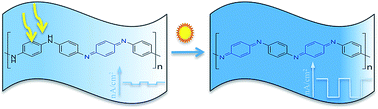
Although polyaniline (PAni) has been studied extensively in the past, little work has been done on producing films of this material via plasma deposition. We have synthesized and analysed the photoresponse behavior of plasma-deposited polyaniline films and proceeded to dope the films using light and with various metal ions. Upon illumination, the photocurrent responses of the thin plasma films increased over time, and the response was dependent on the film thickness. On doping the film with metal ions, the photocurrent densities were enhanced from nano- to micro-amperes per square centimeters. Doping seemed, however, to cause the films to become unstable. Despite this setback, which requires further research, the drastic increase in current shows great promise for the development of plasma-deposited polyaniline films for application in the area of organic electronics and photovoltaics.


Introduction

The development of photosensitive materials based on organic semiconductors has been an attractive approach for energy conversion that uses cheap, abundant and non-toxic materials.1–6 Using organic semiconductors as opposed to their in-organic counterparts,7–10 opens up many options for flexible and robust devices for a fraction of the cost. Organic semiconductors are being pursued to potentially replace the common silicon photovoltaic devices (PV), which currently dominate the market,11,12 or to find use in niche applications.

Polyaniline (PAni) is a conducting polymer and a promising candidate for use in organic opto-/electronics13–17 due to its low production cost, semi-flexibility, bio stability and high conductivity.18–22 To date, polyaniline was most commonly prepared through wet chemical23,24 or electrochemical processes.25–28 Other synthesis methods include inverse emulsion,29 autocatalysis,30 enzymatic31 and photochemical polymerization.32 Many of polyaniline's properties depend on the polymerization process, such as redox state, film thickness and conductivity.

The neutral form of polyaniline has three distinguishable redox states, namely the leucomeraldine base (LB), the emeraldine base (EB) and the pernigraniline base (PNB). As highlighted in Fig. 1 the PNB displays the fully oxidized state of polyaniline, which consists of alternating quinonoid and aromatic aniline units. All nitrogen atoms are deprotonated, with quinonoid and aromatic aniline units alternately linked through the imine bond. The LB is the fully reduced and protonated form, which acts as an insulator. The EB is the half-oxidized form of polyaniline, where half of the nitrogen atoms in the polymer chains are deprotonated (Fig. 1). In principle, there is an infinite number of redox states in between LB, EB and LNB, which explains why polyaniline is a complex material and displays a wide range of properties.4,33


image file: c6ra12886f-f1.tif
Fig. 1 Chemical structures of the main distinguishable redox states of polyaniline in their neutral form: the leucomeraldine base (LB), the emeraldine base (EB) and the pernigraniline base (PNB).

As synthesized, polyaniline usually requires further doping to enhance the conductivity.34–36 Conventional doping methods include acid treatment (known as non-redox doping) and iodine doping (oxidation).35,36 Photo-doping occurs when light with a greater energy than the band gap is used to promote electrons from the valence band into the conduction band, causing subsequent oxidation.

Plasma-enhanced chemical vapour deposition (PECVD) is an alternative method to deposit thin films directly from the vapour phase onto a solid-state substrate.37 When depositing polymeric thin films, the terminology “plasma polymerization” is often used.38 The process is initiated by the application of an alternating electric field across a process vapour comprising volatile organic molecules, which, via a series of chemical reactions in the plasma gas phase, form molecular radicals and ions39 that react with each other to give thin films deposition. PECVD has a distinct advantage over wet chemical methods by producing thin, cohesive homogenous films40 that are highly adherent on a variety of surfaces including glass, metals and a variety of other substrates.41 Plasma polymers are often used as protective coatings.42–45

Plasma polymerization has been used previously in a few studies to deposit thin polyaniline films18,46–48 but the resulting films had inferior properties compared with conventionally synthesized ones. In this article we first optimized the plasma deposition conditions towards improved conductance and then show for the first time that PECVD polyaniline can be photo-doped by exposing the films to one sun equivalent of solar light, responding with enhanced photocurrent densities.

In-depth analysis of the PECVD film by X-ray Photoelectron Spectroscopy (XPS) revealed that the photo-induced doping of plasma-polymerized polyaniline was caused by trans-formation from an originally reduced species of polyaniline to another form with a high extent of oxidation. We also incorporated various metal ions within the film matrix to further enhance or modify the electronic and optical properties.

Materials and methods

Chemicals

Aniline (99.5%), copper(II) chloride hexahydrate, copper(II) sulfate pentahydrate, manganese(II) nitrate tetrahydrate and cobalt(II) nitrate hexahydrate were purchased from Sigma Aldrich and used without further purification. Fluorinated tin oxide (FTO) and gold slides (200 nm Au with 40 nm Ti sublayer on microscope slides, DRLI Inc. USA) were cut into 2.5 × 2.5 cm substrates and cleaned with ethanol (99.5%) and subsequently rinsed with acetone (99.8%) before use.

Methods

Photocurrent measurements were recorded on a PG 310 potentiostat (HEKA, Germany) in a three electrode configured photo electrochemical cell (PEC) using an Abet Solar simulator (Solar Simulator, Abet Technologies, Milford, CT, USA) as artificial light source. The artificial solar light was calibrated against a silicon solar cell (Newport) to 1.5 equivalent of air mass (AM 1.5). The PEC, a homemade Teflon block with integrated quartz window, was filled with a 0.1 M phosphate buffered saline (PBS) electrolyte solution (pH 7.4) and the plasma-polymerized films deposited on conducting substrates (fluorinated tin oxide, FTO, or 100 nm gold on microscope slides) acted as working electrodes (WE). A platinum rod was used as counter electrode (CE); all recorded current densities were referred to Ag|AgCl (3 M KCl). The working electrodes were illuminated with light intensity of 100 mW cm−2 for 12 s dark and 12 s light intervals at their open circuit potentials (OCP).

ToF-SIMS measurements were performed with a PHI TRIFT V nanoTOF instrument (PHI Electronics Ltd, USA). A 30 keV, pulsed primary 197Au+ ion beam was used to sputter and ionize species from each sample surface. PHI's patented dual beam charge neutralization system using a combination of low energy argon ions (up to 10 eV) and electrons (up to 25 eV) was employed to provide charge neutralization. Positive mass axis calibration was done with CH3+, C2H5+ and C3H7+. Spectra were acquired in the bunched mode for 60 seconds from an area of 100 μm × 100 μm. The corresponding total primary ion dose was less than 1 × 10¹² ions cm−2, and thus met the static SIMS regime.49 A mass resolution mm of >7000 at nominal m/z = 27 amu (C2H3+) was typically achieved.

Some samples were characterized by multiple recording of positive ion mass spectra, which were collected from sample areas that did not overlap. All recognizable, clear (i.e. unobscured by overlaps) fragment ions from 2 up to 175 amu were used in calculations. The peaks were normalized to the total intensity of all selected peaks. Multiple mass spectra were processed with the aid of principal component analysis, PCA.50 PCA was performed using PLS_Toolbox version 3.0 (Eigenvector Research, Inc., Manson, WA) along with MATLAB software v. 6.5 (MathWorks Inc., Natick, MA).

X-ray photoelectron spectroscopy was performed with a Kratos AXIS Ultra DLD spectrometer, using monochromatic AlKα radiation ( = 1486.7 eV). The system is equipped with a magnetically confined charge compensation system (low energy electrons are confined and transported to the sample surface by a magnetic field). Spectra were recorded using an acceleration voltage of 15 keV at a power of 225 W. Survey spectra were collected with a pass energy of 160 eV and an analysis area of 300 × 700 μm. High-resolution spectra were obtained using a 20 eV pass energy and an analysis area of 300 × 700 μm. Data analysis was performed with CasaXPS software (Casa Software Ltd). All binding energies were referenced to the “neutral” C 1s peak at 285.0 eV. Core level envelopes were curve-fitted with the minimum number of mixed Gaussian–Lorentzian component profiles. The Gaussian–Lorentzian mixing ratio (typically 30% Lorentzian and 70% Gaussian functions); the full width at half maximum, and the positions and intensities of peaks were left unconstrained to result in a best fit.

The polyaniline coating thicknesses were determined by coating silicon wafers with aniline plasma polymer films in parallel with Au/Ti/glass slides. The measurements were accomplished by using a variable-angle spectroscopic ellipsometer (VASE, J.A. Woolam Co. Inc. NE, USA). Scans over the wavelength region 400–800 nm were performed at three incident angles, viz., 65°, 70° and 75°. The thicknesses of the transparent plasma polymer films were calculated by applying a Cauchy model (silicon + one Cauchy overlayer) using the WVASE32 software (J. A. Woollam Co., Inc., USA).

Synthesis of plasma polymer films

The experimental set-up for the preparation of RF plasma polymerized aniline thin films has been described elsewhere.51,52 In brief, the reactor chamber was defined by a Pyrex glass cylinder with a height of 35 cm and a diameter of 17 cm. It comprised an upper, U-shaped brass electrode and a lower electrode that was a copper disc of 10 cm diameter. The distance between the electrodes was 12.5 cm. The upper electrode was powered by a commercial RF generator (Advanced Energy, RFX 600) connected to a manually operated matching network box to minimize the reflected power. Samples were placed on the lower, grounded electrode. The monomer aniline was placed in a round-bottom flask and connected to the reactor chamber by a stainless steel line via a flow control needle valve. The pumping system consisted of a rotary pump connected to the reactor via a LN2 cold trap and an isolation valve. A base pressure lower than 2 × 10⁻² Torr was achieved in the reactor prior to adding process vapour. The pressure of the monomer vapour prior to initiation of the glow discharge was set at 0.2 Torr. Plasma-deposited polyaniline thin films were synthesized via both continuous and pulsed plasma power settings. The duty cycle during pulsed mode was 1 ms/20 ms. Peak power (P) was varied between 20, 40 and 60 W. Deposition times in the pulsed and continuous modes were 40 and 5 min respectively. The plasma apparatus was placed in a thermostatically controlled laminar flowhood and kept at a temperature of 25–27 °C to maintain a constant pressure and flow of the monomer at 0.2 Torr.

Results and discussion

Preparation of PECVD polyaniline

PECVD has the advantage over conventional chemical vapour deposition (CVD) methods that it generates reactive species (radicals and ions) in the gas phase at low temperatures, thus allowing the deposition of thin films onto temperature-sensitive substrates,53 such as semiconductors for photovoltaics. In principle, increased temperatures also affect the quality of the de-posited film itself, which can result in poor adhesion properties or inhomogeneous surface topology of films. Here we conducted a systematic study of the photo-physical properties of plasma-polymerized polyaniline (PAni-pp) by modifying the deposition mode, film thickness, and time of light exposure to achieve the highest effect of photo-doping. Good control over reproducible deposition of polyaniline thin films was essential and was achieved with a reactor base pressure of 20 mTorr and a monomer temperature of 25–27 °C. We also explored plasma deposition of aniline with the entire plasma system heated to 40 °C inside a flowhood, but this did not result in marked improvements.
Plasma deposition mode. The plasma polymerization of the monomer aniline was found to be highly dependent on the experimental parameters. It is well known that physical and chemical processes in the plasma gas phase can result in extensive fragmentation of the monomer molecule, thus yielding films with scrambled chemical structures that are quite different to conventional polymers from the same monomer.23 Pulsed plasma polymerization often results in marked improvements of retention of monomer structural elements in the film, since in the “on” period the plasma activates radical reactions, which then proceed in a conventional addition mode during the “off” time. One of the objectives of this study was to optimize plasma polymerization process parameters such as duty cycle to achieve maximum retention of the monomer moieties in PAni-pp coatings, since this would be expected to enhance conductivity. In a preliminary study it was established that good control over reproducible film thicknesses was achieved at a plasma power of 20 W. Application of higher powers (40 and 60 W) resulted in the deposition of thicker films but with lesser control of thicknesses. The effect of duty cycle was therefore investigated by applying constant wave (cw) and pulsed (DC = 1 ms/20 ms) modes at 20 W plasma power. The surface chemistry of the resultant polyaniline plasma polymer (PAni-pp) coatings was studied using ToF-SIMS.

Fig. 2 shows positively charged ions, wide range (0–200 amu) static mass spectra for PAni-pp films that were produced using cw (trace a) and pulsed (trace b) plasmas. The spectra were complex and they showed distinct differences, attesting to substantial compositional differences upon using different plasma conditions. Both spectra contain a peak at m/z = 77 amu, which can be assigned to the C6H5+ fragment ion, a fingerprint ion originating from aniline in ToF-SIMS. This is the major fragment in the spectrum for the PAni-pp film obtained using pulsed mode, whilst the spectrum for the constant wave plasma polymer is dominated by multiple low molecular weight fragment ions, mostly assignable to hydrocarbon species.


image file: c6ra12886f-f2.tif
Fig. 2 Positive ion static mass spectra recorded with PAni-pp films generated using: (a) continuous plasma and (b) pulsed plasma, both at plasma power input of 20 W.

Direct comparison of polyaniline coatings is difficult, as the spectral differences are not related to unique peaks but to changes in relative intensities of common peaks. The univariate comparison could be ambiguous, thus we used multivariate principal component analysis (PCA) to aid in the interpretation of the static positive ToF-SIMS spectra. Fig. 3a shows the scores plot on PC1 and PC2 for the positive mass spectra of Fig. 2. The spectra form two well-separated clusters along PC1, which retains almost 99% of the original data variance, making it unnecessary to consider PC2 for further analysis. The specimens are clearly different, but their surfaces are quite uniform/homogeneous, as indicated by the low scatter of the experimental points in each group.


image file: c6ra12886f-f3.tif
Fig. 3 PCA of positive ion static mass spectra for PAni-pp films generated using continuous plasma (cw) and pulsed plasma (DC) at power of 20 W: (a) scores plot on PC1 and PC2; (b) loadings of positive fragment ions on PC1.

Fig. 3b displays loadings of positive fragment ions on PC1, which reveal the causes of observed differences between the samples. The surface of the PAni-pp film prepared with constant wave plasma mode is characterized by positively loaded hydrocarbon fragment ions like CH3+, C2H3+, C3H3+, C3H5+ and also by an aromatic C7H7+ tropylium ion. The surface of PAni-pp films prepared using pulsed plasma, on the other hand, is dominated by fragment ions including C6H5+, C6H8N+, C6H4N2+, C12H12N+ and C12H11N2+ that are indicative of polyaniline. The latter two reflect the presence of aniline dimers. Clearly, under continuous plasma excitation, there is significant loss of amine groups from aniline in the plasma and the resultant film has a higher extent of hydrocarbon character. Thus, pulsed plasma conditions appear to be essential for the optimization of polyaniline-like composition in plasma-deposited polyaniline films. Low power continuous plasmas, such as the 20 W used in this study, have often been used to attempt to reduce monomer fragmentation; for example Cruz et al.46 and Gong et al.47 showed that plasma conditions affected the composition of aniline plasma polymers but did not investigate pulsing. Pulsing in aniline plasma deposition was used by Ameen et al.,48 but they also used higher power (120 W) and did not compare pulsing with continuous plasma operation.

As the ToF-SIMS results indicate that the application of pulsed plasma resulted in higher retention of the monomer structure and thus in less scrambled, more polyaniline-like coatings, PAni-pp films for the photophysical investigations were generated using pulsed 20 W power plasma.

Photo-doping of polyaniline

The effect of photo-induced “self-doping” – or photo-doping – has not been reported with PAni-pp films. It can be understood as a light-induced transformation from a less oxidized form of polyaniline to another form with a higher grade of oxidation.

In our initial studies, transparent PAni-pp films were deposited onto a FTO substrate and observed to possess grain type surface topology with irregular sizes by Scanning Electron Microscopy (SEM, Fig. 4a). Initial photophysical investigations of the PAni-pp films revealed that the films responded with increased negative current densities the more they were exposed to artificial sunlight. Although the FTO substrate itself was intrinsically an electron-donating layer (n-type, Fig. 4b), the photocurrent experiments on the plasma films showed a faint p-type photocurrent response indicating that PAni-pp is a photoactive material. In the course of the chronoamperometric experiments it was noticed that the p-type photocurrent behavior (electron acceptor) became more pronounced when the films were illuminated for longer periods of times. After 30 min total illumination the photocurrent density increased by a factor of 10 (blue, Fig. 4c) at the open-circuit potential (OCP).


image file: c6ra12886f-f4.tif
Fig. 4 (a) SEM image of 160 nm thick PAni-pp deposited onto a FTO substrate via pulsed plasma technique; (b) chronoamperogram of the bare FTO substrate showing FTO as intrinsically n-type material; (c) chronoamperograms of the same PAni-pp film showing increasing p-type photocurrent responses within increasing times (5, 10 and 15 min) of light exposure under 1.5 AM artificial solar light. The photocurrent densities were recorded repetitively under dark and 1.5 AM (100 mW cm−2) solar light for 12 s intervals, where the first, third and fifth 12 seconds record the dark current. All photocurrent responses were recorded at their open-circuit potentials (OCP); (d) photographic picture of the PAni-pp film showing a “dark stain” caused by irradiation with light.

Artificial sunlight enhanced the photophysical properties of the PAni-pp film as a p-type semiconductor, causing doping effects in the thin polyaniline film (photo-doping). The photo-oxidation of the PAni-pp film could be observed with the naked eye. The area of the initially semi-transparent PAni-pp film that was exposed to light during chronoamperometric measurements underwent a visible change in colour (dark stain), as shown in Fig. 4d.

IR spectroscopic investigations could not provide clear insights into the photo-oxidation at a molecular level when we compared the illuminated and non-illuminated areas by ATR-IR spectroscopy (Fig. 5).

Both areas showed under ATR-IR spectroscopy two dominant vibrational bands at 1596 cm−1 and 1495 cm−1 accompanied by weak C–C bending modes at 748 and 605 cm−1, two weak bands at 1309 and 1250 cm−1 and C–H, N–H as well as absorbed water molecules in the range 2800–3500 cm−1. A clear discrimination between the different redox states of the as-synthesised PAni-pp film under ATR-IR was difficult, and we infer that our PAni-pp contained both forms. For the assignments of the detected vibrational bands different species of PAni-pp came into consideration. Both major bands at 1596 and 1495 cm−1 are reported to originate from the benzene (N–benzene–N) and (N[double bond, length as m-dash]quinonoid[double bond, length as m-dash]N) rings of the EB structures (EB, Fig. 1).54 On the other hand, the presence of short LB oligomers is reported to cause the vibrational bands at 1596, 1495 and 1309 cm−1.55 It is likely that the PECVD method caused trapping of reactive intermediates of the LB oligomer in the polymer matrix. As additional complexity the LB polymer itself is known to show intense vibrational bands at 1596 cm−1 and, the two weak bands at 1309 cm−1 (CAr–N) and 1250 cm−1 (C–N˙+) are assigned to bipolaron structures.54,56


image file: c6ra12886f-f5.tif
Fig. 5 ATR-IR spectra of the illuminated and non-illuminated areas of the PAni-pp film. Insets with different frame colors represent expanded ranges in the full IR spectrum.

X-ray photoelectron spectroscopy (XPS) was used to unravel the effect of photo-induced doping on plasma polymerized polyaniline films and it was also investigated whether the film thickness plays a role.

Film thickness. The vapour pressure of aniline is low compared to conventional monomers used in plasma polymerization. Consequently, when plasma is initiated the base pressure decreases, which is indicative of monomer consumption. Since the pulsed plasma technique allowed good control over the monomer consumption (see experimental details), the film thickness could be controlled by adjusting the deposition time. PAni-pp films with thicknesses of 25 nm, 40 nm, 80 nm and 160–200 nm were produced. Since FTO behaved as an intrinsically n-type substrate, all films were deposited onto a 100 nm gold layer (above 40 nm Ti on microscope slides), as a p-type material due to its photoelectric effect. All films were exposed to artificial solar light for 5 minutes before chronoamperometric measurements were undertaken.

Fig. 6a shows the photocurrent responses upon illumination with artificial solar light (AM 1.5). The thinner films with 25 and 40 nm thicknesses responded with higher current densities, where the highest photocurrent responses were achieved with −540 nA cm−2 with the 40 nm PAni-pp layer. The thicker layers of PAni-pp, however, responded with lower current densities, well below −100 nA cm−2, suggesting that limiting penetration depth of light and increasing ohmic resistance with increasing film thicknesses were causing a drop of electron mobility that resulted in poorer photocurrent responses. The ideal film thickness was found to be 25–40 nm to obtain a high-performing organic semiconductor based on plasma polymerized polyaniline films.


image file: c6ra12886f-f6.tif
Fig. 6 (a) Chronoamperograms of four different PAni-pp films with 25, 40, 80 and 160 nm thickness. The photocurrent densities were recorded repetitively under dark and 1.5 AM (100 mW cm−2) solar light in 12 second intervals, where the first, third and fifth 12 seconds record the dark currents. All photocurrent responses were recorded at their open-circuit potentials (OCP) vs. Ag/AgCl (3 M KCl); (b) photocurrent responses of four different PAni-pp films with 25, 40, 100 and 160 nm thicknesses under continuous exposure to 100 mW cm−2 (1.5 AM) for up to 4 hours; the current densities were recorded at their OCP against Ag|AgCl (3 M KCl) in 0.1 M PBS solution.

For comparisons, an electropolymerised PAni film (PAni-ep) was grown on a gold substrate under acidic conditions and its photocurrent behaviour was analysed towards exposure to artificial sunlight. The cyclic voltammogram of the PAni-ep film growth and its chronoamperogram are depicted in Fig. S1 (ESI). The PAni-ep responded with lower and less consistent p-type photocurrents ranging between −175 and −183 nA cm−2. Additional OCP drifts of PAni-ep during photocurrent measurements and prolonged times required for both steady states in the dark- and photocurrents clearly highlight the advantage of PAni-pp thin films obtained via our PECVD technique.

Long-term exposure of PAni-pp to solar light. The photo-induced doping of PAni-pp was initiated once the film was exposed to 1.5 AM artificial solar light, resulting in an organic semiconductor with p-type behavior. As a consequence of these observations, we conducted long-term expo-sure experiments of PAni-pp with four different film thicknesses for up to four hours. The PAni-pp films were deposited on gold substrates and their thicknesses were ellipsometrically determined to be 25, 40, 100 and 160 nm.

Fig. 6b shows the chronoamperograms of selected films under continuous irradiation. Again, the thicker films, 160 and 100 nm, responded with lower current densities under continuous exposure to light whilst the 100 nm film showed notable current responses of more than −400 nA cm−2 after 2.5 hours. Note, that the steady state was still not achieved, suggesting that longer times of light exposure are needed. In contrast, steady state was already achieved after 100 min with the 25 nm film, resulting in similar photocurrent densities. The highest photocurrent responses were obtained from 40 nm films, with highest current densities of −800 nA cm−2 after 2.5 h. Again, the 40 nm PAni-pp film showed the best performance among the series showing no significant loss after 4 h in total. Hence, all PAni-pp films subjected to further analysis were produced with 40 nm thicknesses.

X-ray photoelectron spectroscopy analysis. To understand the photo-induced doping effect of PAni-pp films on a molecular level, 40 nm PAni-pp films were deposited onto Au/Ti/glass and subjected to surface analysis by XPS. The untreated sample and its homologues after exposure to 1.5 AM artificial sunlight in the photoelectrochemical cell for 5 min and 3 h were examined. The survey spectra before and after illumination revealed differences in elemental compositions, as summarized in Table 1.
Table 1 XPS elemental composition for 40 nm PAni-pp films on Au/Ti/glass slide prior to and after 5 and 180 min of irradiation with 1.5 AM artificial sunlight, respectively
Irradiation time, min Composition, at%
O N C
a 5 min and 180 min irradiated specimens showed also presence of 1.0 at% of Si and 0.5 at% of Au respectively.
0 3.5 10.1 86.4
5a 7.1 8.6 83.3
180a 10.9 8.1 80.4


The control sample showed 3.5 at% of oxygen, which doubled upon the first 5 min of irradiation. Prolonged exposure to artificial sunlight resulted in a further increase in the oxygen content, which reached a value of 11.0 at% after 3 h. The XPS results thus revealed oxygen incorporation into the PAni-pp coating upon irradiation. The rate of the reaction changed with time. The initial irradiation period resulted in fast initial oxidation, whose rate dropped distinctly, likely exponentially, with time. Fig. 7 shows high-resolution C 1s core level spectra prior to (trace a) and after 3 hours of illumination (trace b).


image file: c6ra12886f-f7.tif
Fig. 7 High resolution component fitted C 1s and N 1s core level spectra for 40 nm PAni-pp film on Au/Ti/glass slide: (a) C 1s for untreated coating; (b) C 1s for coating irradiated for 3 h with 1.5 AM artificial sunlight; (c) N 1s for untreated coating; (d) N 1s for coating irradiated for 3 h with 1.5 AM artificial sunlight.

The assignments of the fitted components and the compositions of the C 1s levels are summarized in Table 2. The untreated PAni-pp control consisted of four types of carbon environments. The CC/CH (sp3) and C–N components accounted for 69.5 and 21.8% of the total C 1s envelope respectively. The values diverged from the theoretical stoichiometry of polyaniline due to the complexity of propagating species present in a gas discharge during plasma polymerization. The presence of C–O and C[double bond, length as m-dash]O components, at 6.9 and 1.9% respectively, indicates that the surface was lightly oxidized during the plasma coating fabrication and (or) after that, upon exposure to air, as has been observed for other amine plasma-deposited coatings.57–59

Table 2 Compositions of C 1s and N 1s core level spectra for untreated 40 nm PAni-pp film on Au/Ti/glass slide and after its irradiation with 1.5 AM artificial sunlight for 180 min
Irradiation time (min)  
C 1s peaks assignment (BE, eV)
  284.0 285.0 286.0 286.6 288.0 289.8
  C[double bond, length as m-dash]C C–C/C–H C–N C–O C[double bond, length as m-dash]O O–C[double bond, length as m-dash]O
[thin space (1/6-em)]
C 1s envelope composition, % (total = 100)
0 0 69.5 21.8 6.9 1.9 0
180 24.9 41.9 14.5 11.1 4.9 2.6

Irradiation time (min)  
N 1s peaks assignment (BE, eV)
  398.0 399.8 400.8
  –N[double bond, length as m-dash] –NH– –HN+
[thin space (1/6-em)]
N 1s envelope composition, % (total = 100)
0 9.0 79.5 11.5
180 28.2 51.2 20.6


After three hours of illumination the chemical composition of PAni-pp had changed. The C 1s spectrum showed 6 components which were assigned (Table 2) to C[double bond, length as m-dash]C (sp2), C–C/C–H, C–N, C[double bond, length as m-dash]O and COO environments. The appearance of a peak at 284.0 eV, which corresponded to an unsaturated carbon environment (sp2), was likely to be primarily responsible for the PAni-pp coating's conductivity.

Since nitrogen plays the key role in PAni structures, being the bridging atom in the polymer chain and the redox mediator between polymer units, the N 1s core level spectra are of particular value. Fig. 7c shows that prior to illumination, nitrogen was mainly present in the form of amine bonds (79.5% in Table 2) with small amounts of imine and amine polaron components. The composition of the N 1s spectrum reflects the insulating benzenoid/aromatic character of the PAni-pp coating.60–63 It appears that prior to illumination the PAni-pp film mainly comprised a structure similar to leucoemeraldine base with admixtures of the emeraldine base (Fig. 1). After 3 hours of irradiation the content of insulating amine bonds had decreased by ∼30% and that phenomenon was accompanied by increased formation of imine N and amine polarons. An increase in amine polarons content from 11.5 to 20.6% implies a more conductive polymer. A marked increase in the amount of imine present reinforced the idea that unsaturation led to higher conductivity, meaning the irradiated Pani-pp films could be classed as alike to an emeraldine base. The composition ratio between imine bonds and amines groups (including polarons) in Table 2 is 28.2/71.8 approaching the highest conductive state of PAni, which typically consists of 25/75 quinonoid to benzoid components.

Doping PECVD polyaniline with metal ions

Doping polyaniline with metal salts has already been systematically studied and used in manifold applications.64–67 However, there is little known on the photophysical behavior on polyaniline doped with metal salts. More precisely, doping PAni-pp with transition metal salts and investigating the photocurrent behavior of the resulting metallopolymers has, to the best of our knowledge, not been reported yet.

Incorporation of various metal ions into the polymeric matrix was achieved through incubating the thin films in a 0.01 M solution of Mn(NO3)2, Co(NO3)2, CuSO4 or CuCl2 for three days. These metals were chosen as they display interesting redox chemistry, which potentially can be exploited for catalytic activity. These metals are cheap and abundant and are known to have a high affinity for nitrogen-containing ligands. The solutions were kept in the dark for the duration of binding. Enhanced photocurrents were observed with all samples, as shown in Fig. 8. The highest photocurrent response results from CuCl2 doping, with a current density more than −3 μA cm−2, which is almost double that of its sulfate analogue. The nitrate salts of Co(II) and Mn(II) both showed a photocurrent response at −1 μA cm−2.


image file: c6ra12886f-f8.tif
Fig. 8 Chronoamperograms of four different 40–45 nm PAni-pp samples decorated with 0.01 M aqueous solution of Mn(NO3)2, Co(NO3)2, CuSO4 and CuCl2 for 3 days. The photocurrent responses were recorded at their OCP in 0.1 M phosphate buffered saline solution in a three-electrode configured electrochemical cells using PAni/M substrate as working electrode, a Pt rod as counter electrode and Ag/AgCl (3 M KCl) as reference electrode. The first, third and fifth 12 s record the dark current.

All of the transition metal ions used in this study have different stable oxidation states (for example, cobalt is relatively stable in the oxidation states II and III). A possible explanation for the increase in photocurrent density is photo-activated electron transfer from the metal ions to the polyaniline backbone. Also, the metals centres could act as relays for electrons “hopping” between polyaniline fragments, thus increasing the overall conductivity and photocurrent density. Most likely, a combination of these two effects is the reason for the observed effect.

Ellipsometry results (Table 3) showed that the films degraded with time. Film thicknesses changed and delamination occurred. While photo-oxidation increased the conductivity of the films as discussed above, it resulted in degradation of the polyaniline when doped with transition metal centres. Further study is needed to investigate how this might be overcome or a suitable compromise in performance achieved.

Table 3 Ellipsometry data showing the effect of illumination on PAni film thickness
Treatment Substrate Average thickness (nm)
Control Silicon 40.8
Sample 1 – untreated Gold 44.9
Sample 1 – 5 mins Gold 40.5
Sample 2 – untreated Gold 43.5
Sample 2 – 3 hours Gold 16.9


Conclusions

We successfully plasma polymerized polyaniline (PAni-pp) films with high structural retention when pulsing was used for the plasma excitation, and explored the thin films as potential candidates as organic semiconductor with p-type properties (electron acceptor). Chronoamperometric investigations revealed that these films increase their performances as photoactive semiconductor when irradiated with artificial sunlight (photo-doping or photo-induced doping). Analysis by XPS prior to illumination and after long-term exposure to one equivalent of sunlight allowed us to understand the photo-doping effect as light-triggered transformation from a reduced form of polyaniline to another form with higher grades of oxidation. These unique properties of thin PAni-pp films becoming active just by switching on light offers promise for applications in sensor, photocatalysis, adhesive interlayers for immobilized photocatalysts68 or optoelectronic materials where light plays a crucial role. Usually, chemical modification or harsh chemical conditions such as strong acids and oxidants are required to dope polyaniline films. Here, exposure to light suffices to achieve the film doping by itself, which has never been described before.

After doping the PECVD polyaniline with various transition metals, the films displayed an enhanced photocurrent response; however, the long-term stability of films was drastically decreased. Transition metal doped PECVD polyaniline would have huge potential as an inexpensive and efficient photocatalytic materials for many applications, if a solution to increase the long-term stability can be found in future research.

Acknowledgements

This work was performed (in part) at the South Australian node of the Australian National fabrication Facility (ANFF-SA) under the National Collaborative Research Infrastructure Strategy to provide nano and microfabrication facilities for Australia's researcher.

Notes and references

  1. T. P. Yoon, M. A. Ischay and J. Du, Nat. Chem., 2010, 2, 527–532 CrossRef CAS PubMed.
  2. L. Schmidt-Mende, A. Fechtenkotter, K. Mullen, E. Moons, R. H. Friend and J. D. MacKenzie, Science, 2001, 293, 1119–1122 CrossRef CAS PubMed.
  3. J. Yan, T. Wei, B. Shao, Z. Fan, W. Qian, M. Zhang and F. Wei, Carbon, 2010, 48, 487–493 CrossRef CAS.
  4. E. Song and J.-W. Choi, Nanomaterials, 2013, 3, 498 CrossRef CAS.
  5. A. G. MacDiarmid, Angew. Chem., Int. Ed., 2001, 40, 2581–2590 CrossRef CAS.
  6. S. R. Forrest, Nature, 2004, 428, 911–918 CrossRef CAS PubMed.
  7. W.-T. Sun, Y. Yu, H.-Y. Pan, X.-F. Gao, Q. Chen and L.-M. Peng, J. Am. Chem. Soc., 2008, 130, 1124–1125 CrossRef CAS PubMed.
  8. S. Chandrasekaran, T. J. Macdonald, Y. J. Mange, N. H. Voelcker and T. Nann, J. Mater. Chem. A, 2014, 2, 9478–9481 CAS.
  9. T. J. Macdonald, J. Xu, S. Elmas, Y. J. Mange, W. M. Skinner, H. Xu and T. Nann, Nanomaterials, 2014, 4, 256–266 CrossRef.
  10. D. P. Tran, T. J. Macdonald, B. Wolfrum, R. Stockmann, T. Nann, A. Offenhaeusser and B. Thierry, Appl. Phys. Lett., 2014, 105, 231116 CrossRef.
  11. S. E. Shaheen, D. S. Ginley and G. E. Jabbour, MRS Bull., 2005, 30, 10–19 CrossRef CAS.
  12. C. J. Brabec, Sol. Energy Mater. Sol. Cells, 2004, 83, 273–292 CrossRef CAS.
  13. A. Pron and P. Rannou, Prog. Polym. Sci., 2002, 27, 135–190 CrossRef CAS.
  14. Y. Yang, J. Ouyang, L. Ma, R. J.-H. Tseng and C.-W. Chu, Adv. Funct. Mater., 2006, 16, 1001–1014 CrossRef CAS.
  15. K. Gurunathan, A. V. Murugan, R. Marimuthu, U. Mulik and D. Amalnerkar, Mater. Chem. Phys., 1999, 61, 173–191 CrossRef CAS.
  16. P. Lin and F. Yan, Adv. Mater., 2012, 24, 34–51 CrossRef CAS PubMed.
  17. G. Gustafsson, Y. Cao, G. M. Treacy, F. Klavetter, N. Colaneri and A. J. Heeger, Nature, 1992, 357, 477–479 CrossRef CAS.
  18. T. Barman, A. R. Pal and J. Chutia, Appl. Surf. Sci., 2014, 313, 286–292 CrossRef CAS.
  19. Y. Cao, J. Qiu and P. Smith, Synth. Met., 1995, 69, 187–190 CrossRef CAS.
  20. R. C. Chatelier, C. J. Drummond, D. Y. C. Chan, Z. R. Vasic, T. R. Gengenbach and H. J. Griesser, Langmuir, 1995, 11, 4122–4128 CrossRef CAS.
  21. D. Liu, X. Wang, J. Deng, C. Zhou, J. Guo and P. Liu, Nanomaterials, 2015, 5, 1034 CrossRef CAS.
  22. D.-W. Wang, F. Li, J. Zhao, W. Ren, Z.-G. Chen, J. Tan, Z.-S. Wu, I. Gentle, G. Q. Lu and H.-M. Cheng, ACS Nano, 2009, 3, 1745–1752 CrossRef CAS PubMed.
  23. J. Huang, S. Virji, B. H. Weiller and R. B. Kaner, J. Am. Chem. Soc., 2003, 125, 314–315 CrossRef CAS PubMed.
  24. S. Bhadra, D. Khastgir, N. K. Singha and J. H. Lee, Prog. Polym. Sci., 2009, 34, 783–810 CrossRef CAS.
  25. E. M. Geniès, A. Boyle, M. Lapkowski and C. Tsintavis, Synth. Met., 1990, 36, 139–182 CrossRef.
  26. W.-S. Huang, B. D. Humphrey and A. G. MacDiarmid, J. Chem. Soc., Faraday Trans. 1, 1986, 82, 2385 RSC.
  27. D.-W. Wang, F. Li, J. Zhao, W. Ren, Z.-G. Chen, J. Tan, Z.-S. Wu, I. Gentle, G. Q. Lu and H.-M. Cheng, ACS Nano, 2009, 3, 1745–1752 CrossRef CAS PubMed.
  28. D. Sazou and C. Georgolios, J. Electroanal. Chem., 1997, 429, 81–93 CrossRef CAS.
  29. R. Y. Suckeveriene, G. Mechrez, O. H. Filiba, S. Mosheev and M. Narkis, J. Appl. Polym. Sci., 2013, 128, 2129–2135 CAS.
  30. S. Mu and J. Kan, Electrochim. Acta, 1996, 41, 1593–1599 CrossRef CAS.
  31. M. R. Nabid, Z. Zamiraei and R. Sedghi, Iran. Polym. J., 2010, 19, 699–706 CAS.
  32. F. Koyama and T. Kawai, Dyes Pigm., 2013, 98, 323–326 CrossRef CAS.
  33. E. T. Kang, K. G. Neoh and K. L. Tan, Prog. Polym. Sci., 1998, 23, 277–324 CrossRef CAS.
  34. T. Barman and A. R. Pal, Solid State Sci., 2013, 24, 71–78 CrossRef CAS.
  35. J.-C. Chiang and A. G. MacDiarmid, Synth. Met., 1986, 13, 193–205 CrossRef CAS.
  36. A. G. MacDiarmid and A. J. Epstein, Synth. Met., 1994, 65, 103–116 CrossRef CAS.
  37. L. Martinu and D. Poitras, J. Vac. Sci. Technol., A, 2000, 18, 2619 CAS.
  38. R. D'Agostino and Wiley InterScience (Online service), Advanced plasma technology, Wiley-VCH, Weinheim, Chichester, 2008 Search PubMed.
  39. A. Michelmore, C. Charles, R. W. Boswell, R. D. Short and J. D. Whittle, ACS Appl. Mater. Interfaces, 2013, 5, 5387–5391 CAS.
  40. J. G. Wang, K. G. Neoh and E. T. Kang, Thin Solid Films, 2004, 446, 205–217 CrossRef CAS.
  41. A. M. Mathew and P. Predeep, Polym. Compos., 2013, 34, 1091–1098 CrossRef CAS.
  42. C. J. Hall, P. J. Murphy and H. J. Griesser, Plasma Processes Polym., 2015, 12, 555–563 CrossRef CAS.
  43. M.-G. Mureşan, A. C. Campbell, P. Ondračka, V. Buršíková, V. Peřina, T. Polcar, S. Reuter, M. U. Hammer, M. Valtr and L. Zajíčková, Surf. Coat. Technol., 2015, 272, 229–238 CrossRef.
  44. C. J. Hall, P. J. Murphy, T. Schmauder and H. J. Griesser, Surf. Coat. Technol., 2014, 259, 616–624 CrossRef CAS.
  45. L. Martinu, M. R. Wertheimer and J. E. Klemberg-Sapieha, MRS Proceedings, 1998, 544 Search PubMed.
  46. G. Cruz, J. Morales, M. Castillo-Ortega and R. Olayo, Synth. Met., 1997, 88, 213–218 CrossRef CAS.
  47. X. Gong, L. Dai, A. W. H. Mau and H. J. Griesser, J. Polym. Sci., Polym. Chem. Ed., 1998, 36, 633–643 CrossRef CAS.
  48. S. Ameen, M. Song, D.-G. Kim, Y.-B. Im, H.-K. Seo, Y. S. Kim and H.-S. Shin, Macromol. Res., 2012, 20, 30–36 CrossRef CAS.
  49. D. Briggs, Surface analysis of polymers by XPS and static SIMS, Cambridge University Press, Cambridge, New York, Digitally printed 1st pbk. version, 2005 Search PubMed.
  50. M. Jasieniak, D. Graham, P. Kingshott, L. Gamble and H. Griesser, in Handbook of Surface and Interface Analysis, ed. J. Rivière and S. Myhra, CRC Press, 2009, pp. 529–564 Search PubMed.
  51. H. J. Griesser, Vacuum, 1989, 39, 485–488 CrossRef CAS.
  52. A. M. Sandstrom, M. Jasieniak, H. J. Griesser, L. Grøndahl and J. J. Cooper-White, Plasma Processes Polym., 2013, 10, 19–28 CrossRef CAS.
  53. F. Massines, C. Sarra-Bournet, F. Fanelli, N. Naudé and N. Gherardi, Plasma Processes Polym., 2012, 9, 1041–1073 CrossRef CAS.
  54. M. Trchová, J. Stejskal and J. Prokeš, Synth. Met., 1999, 101, 840–841 CrossRef.
  55. S. Quillard, G. Louarm, J. P. Buisson, S. Lefrant, J. Masters and A. G. MacDiarmid, Synth. Met., 1992, 49–50, 525–530 CrossRef.
  56. S. Quillard, G. Louam, J. P. Buisson, M. Boyer, M. Lapkowski, A. Pron and S. Lefrant, Synth. Met., 1997, 84, 805–806 CrossRef CAS.
  57. T. R. Gengenbach, R. C. Chatelier and H. J. Griesser, Surf. Interface Anal., 1996, 24, 271–281 CrossRef CAS.
  58. T. R. Gengenbach, R. C. Chatelier and H. J. Griesser, Surf. Interface Anal., 1996, 24, 611–619 CrossRef CAS.
  59. T. R. Gengenbach and H. J. Griesser, J. Polym. Sci., Polym. Chem. Ed., 1999, 37, 2191–2206 CrossRef CAS.
  60. S. Golczak, A. Kanciurzewska, M. Fahlman, K. Langer and J. J. Langer, Solid State Ionics, 2008, 179, 2234–2239 CrossRef CAS.
  61. A. P. Monkman, G. C. Stevens and D. Bloor, J. Phys. D: Appl. Phys., 1991, 24, 738–749 CrossRef CAS.
  62. J. B. Metson, Surf. Interface Anal., 1999, 27, 1069–1072 CrossRef CAS.
  63. H. Sangodkar, S. Sukeerthi, R. S. Srinivasa, R. Lal and A. Q. Contractor, Anal. Chem., 1996, 68, 779–783 CrossRef CAS PubMed.
  64. O. P. Dimitriev, Macromolecules, 2004, 37, 3388–3395 CrossRef CAS.
  65. C. M. S. Izumi, V. R. L. Constantino, A. M. C. Ferreira and M. L. A. Temperini, Synth. Met., 2006, 156, 654–663 CrossRef CAS.
  66. C. M. S. Izumi, A. M. D. C. Ferreira, V. R. L. Constantino and M. L. A. Temperini, Macromolecules, 2007, 40, 3204–3212 CrossRef CAS.
  67. D. Li, J. Huang and R. B. Kaner, Acc. Chem. Res., 2009, 42, 135–145 CrossRef CAS PubMed.
  68. S. Elmas, F. Ambroz, D. Chugh and T. Nann, Langmuir, 2016, 32, 4952–4958 CrossRef CAS PubMed.

Footnote

Electronic supplementary information (ESI) available. See DOI: 10.1039/c6ra12886f

This journal is © The Royal Society of Chemistry 2016
Click here to see how this site uses Cookies. View our privacy policy here.