Experimental and theoretical study of the electronic structure and optical spectral features of PbIn6Te10

A. H. Reshak*ab, Oleg. V. Parasyukc, H. Kamarudinb, I. V. Kitykd, Zeyad A. Alahmede, Nasser S. AlZayede, Sushil Auluckfg, Anatolii O. Fedorchukh and J. Chyskýi
aNew Technologies – Research Centre, University of West Bohemia, Univerzitni 8, 306 14 Pilsen, Czech Republic. E-mail: maalidph@yahoo.co.uk
bCenter of Excellence Geopolymer and Green Technology, School of Material Engineering, University Malaysia Perlis, 01007 Kangar, Perlis, Malaysia
cLviv National University of Veterinary Medicine and Biotechnologies, Pekarska Street 50, 79010 Lviv, Ukraine
dFaculty of Electrical Engineering, Czestochowa University Technology, Armii Krajowej 17, PL-42201, Czestochowa, Poland
eDepartment of Physics and Astronomy, College of Science, King Saud University, P.O. Box 2455, Riyadh 11451, Saudi Arabia
fCouncil of Scientific and Industrial Research – National Physical Laboratory, Dr. K S Krishnan Marg, New Delhi 110012, India
gDepartment of Physics, Indian Institute of Technology, Hauz Khas, New Delhi 110016, India
hUniversity of Veterinary and Biotechnology, Lviv, Pekarska 50, Ukraine
iDepartment of Instrumentation and Control Engineering, Faculty of Mechanical Engineering, CTU in Prague, Technicka 4, 166 07 Prague 6, Czech Republic

Received 17th May 2016 , Accepted 23rd July 2016

First published on 25th July 2016


Abstract

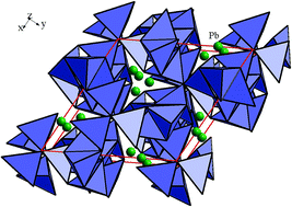
We present measurements of the optical properties of crystalline PbIn6Te10. The samples are grown in the form of parallelepipeds of size ∼5 × 3 × 0.3 mm3. The absorption coefficient α() shows an exponential behavior with energy in the energy range 0.82–0.99 eV followed by an abrupt increase in the absorption from 1.07–1.13 eV. According to the analysis of the data, the indirect gap is 0.88 eV while the direct gap is 1.05 eV. We have used our own measured X-ray diffraction data of the atomic positions in the unit cell as the input for the first principles calculations. Using the generalized gradient approximation (PBE − GGA) within the full potential linear augmented plane wave (FPLAPW + lo) method, the atomic positions are relaxed so as to minimize the forces acting on the atoms. We have used this relaxed geometry to calculate the electronic structure and related ground state properties using PBE − GGA and a recently modified Becke–Johnson potential (mBJ) and mBJ with spin–orbit coupling (mBJ + soc). The analysis of band energy dispersion shows that the valence band maximum (VBM) is located at Γ symmetry points, while the conduction band minimum (CBM) is situated at the M symmetry point of the first Brillouin zone, resulting in an indirect energy band gap of about 0.5 eV (PBE − GGA), 0.8 eV (mBJ) and 0.5 eV (mBJ + soc). It is clear that mBJ succeeds by a large amount in bringing the calculated energy gap in good agreement with the measured energy gap of 0.9 eV. However the inclusion of spin–orbit coupling modifies strongly the CBM and reduces the band by 0.3 eV. The anisotropy of space charge density distribution is analyzed with respect to the charge density distribution.


1. Introduction

The study of lead telluride based single crystals is an important area of research both from a fundamental point of view and because of its use in optoelectronic applications. From the fundamental solid state physics aspect these crystals are of particular interest due to their large phonon anharmonicity,1 which has a substantial influence on the optoelectronic properties. At the same time due to the wide transparency in the infra-red (IR) region their optoelectronic features are very useful for applications.2 The lattice anharmonicity results in anharmonic phonons which possess asymmetry described by third rank polar tensors, similarly to effects of second harmonic generation, linear electro-optics, piezo-electricity etc. Additionally they possess promising thermal conductivity, photo-stimulated thermal expansion and temperature dependent elastic constants.3 Moreover, these compounds have recently shown promise as perfect models for numerical and experimental probing of anharmonic lattice dynamics and its relation with electronic transport in the IR spectra. Hence we can expect a coexistence of optoelectronic and photo-thermal effects. This may open a new area in applications of these compounds as multi-functional materials.

One of the principal factors which substantially restrains their applications in the mid-IR and in thermo-electrical devices is a large number of defects which interact with the phonon subsystem4 substantially enhancing photo-thermal heating. Of particular importance is the cationic substitution which may tailor the energy gaps and carrier mobility to desirable values.5 Moreover these substitutions may lead to enhanced polarizability of the anionic clusters defining the principal linear and nonlinear optical susceptibility dispersions.6 Following the equilibrium phase diagram for the PbTe–In2Te3 (ref. 6) it is melt congruently at 903 K and possesses a homogenous phase range within 70–83% mol of In2Te3. Its crystalline structure was determined by Deiseroth and Müller7 who found it to be trigonal (space group R32, a = 1.4971 nm, c = 1.8505 nm). The crystals were grown by the Bridgman–Stockbarger6 method. These crystals are transparent in the 1.5–30 μm spectral range8 with absorption coefficient which does not exceed 0.5 cm−1. The refractive index varies within 3–3.2. The magnitude of the experimental second order susceptibility tensor is about 51 pm V−1. This is substantially higher than for the single crystals of AgGaS2 (13 pm V−1) and AgGaSe2 (33 pm V−1). Generally the PbIn6Te10 single crystals could be very interesting materials for studies of the second-order nonlinear optical effects due to the presence of highly polarizable heavy cations, large phonon anharmonicity and charge density acentricity of the telluride anions.9 Also the lead cations, are expected to have charge density acentricity due to the presence of a lone pair.10,11 Another interesting point could be the existence of intrinsic cationic defects which may cause local enhancement of the local Lorentz field responsible for the optical susceptibilities. At the same time differences in mobility for different Brillouin Zone (BZ) directions may be substantial for the determination of charge transfer responsible for the corresponding hyperpolarizability. The further improvement of the nonlinear optical efficiency and photo-thermal parameters requires optimization of the charge density acentricity. These factors favor a detailed study of the band structure and carrier dispersion and related effective masses which define the photo carrier transport and mobility.

The main goal of this work is to establish some relations between the band structure features and the carrier mobility, anisotropy of the effective masses, etc. After comparison with the experimental optical data one can evaluate the role of defect states and their influence on perfect long-range ordered band states. Of principal importance is the role of the phonons and the type of the energy gap (direct and indirect). Such knowledge may give interesting inputs which can help to design better materials for devices.

2. Experimental

For performing the optical measurements the samples were made in the form of parallelopipeds of size ∼5 × 3 × 0.3 mm3. The ohmic contacts were deposited using gallium indium eutectic. These can exist in the large temperature and tension ranges. The temperature was stabilized with accuracy up to 0.1 K using UTREX thermo stabilizer. The optical spectra features were measured using monochromator MDR-208 with silicon (200–1100 nm) and lead sulphide (1000–3000 nm) cooled photodetectors of spectral resolution 0.5 nm. The measurements were carried out on different points of the surface to obtain better statistics. The surfaces of the samples were cut and polished to obtain surface roughness better than 2 μm.

3. Crystal growth

The title crystals were grown using Bridgman–Stockbarger method. For the growth we have used high purity elements (Pb – 99.999 wt%, In – 99.9999 wt%, Te – 99.9999 wt%) which were put in stoichiometric ratios in a fused quartz crucible. This ternary compound melts congruently (903 K).7 For the synthesis of the initial alloys vacuum evaporated container was put at the bottom part of the heater and was heated up to 1070 K at rate 30 K h−1. After keeping of the melt content for 6 hours the heater was switched off. After 6 hours the cooled furnace was excluded from the container and transferred to a two zone furnace. The temperature of the growth band was about 1070 K, and annealing zone ∼720 K. The temperature gradient on the border of crystallization was 3 K mm−1. After finishing the crystallization process the crystal was moved in the annealing zone (annealing for 100 hours). After this process it was shifted and annealed at a rate of 100 K day−1. The final crystal was in a form of a single crystalline cylinder of length 30 mm and diameter 12 mm (see Fig. 1(a)).
image file: c6ra12734g-f1.tif
Fig. 1 (a) As-grown single crystal of PbIn6Te10. (b) Experimental and theoretical diffraction patterns of the PbIn6Te10 crystals and their difference.

4. Crystal structure

The crystalline structure of PbIn6Te10 was established in the ref. 7. The structure was identified by X-ray diffractometer DRON 4-13 with Cu Kα irradiation source and a Ni filter. Rietveld method was applied within the framework of the program WinCSD.12 The refined crystallographic parameters for PbIn6Te10 are presented in Table 1 and Fig. 1(b). The principal crystalline structure may be represented as laying tetrahedral tellurium atoms surrounding In cations (see Fig. 2).
Table 1 Crystallographic data for PbIn6Te10 (R32 (no. 155); a = 14.9789(5), c = 18.631(1) Å; cell volume (Å3) = 3620.2(4); calculated density (g cm−3) = 5.9773(7)). In addition we present the optimized atomic positions which show close agreement with experimentally determined positions from XRD
Elements Wyck. x exp. x opt. y exp. y opt. z exp. z opt. Occ. B
Pb 9d 0.7410(4) 0.7408 0 0 0.259 0.2589 0.667 2.9(2)
In1 18f 0.0897(3) 0.0895 0.3404(3) 0.3401 0.0860(3) 0.0861 1 0.96(15)
In2 18f 0.1905(2) 0.1903 0.0808(2) 0.0806 0.2356(3) 0.2354 1 0.91(15)
Te1 6c 0 0 0 0 0.1630(4) 0.1629 1 1.2(2)
Te2 9d 0.1657(3) 0.1655 0 0 0 0 1 1.8(2)
Te3 9e 0.5927(3) 0.5925 0 0 1/2 1/2 1 0.8(2)
Te4 18f 0.1838(3) 0.1839 0.1387(3) 0.1385 0.3750(2) 0.3748 1 0.9(2)
Te5 18f 0.1030(2) 0.1031 0.3015(3) 0.3013 0.2319(2) 0.2317 1 1.06(15)


image file: c6ra12734g-f2.tif
Fig. 2 Laying of InTe4 tetrahedra in the structure of the compound PbIn6Te10.

Inter-atomic distances are shown in Fig. 3. The lead atoms occupy a part of octahedral voids between the tellurium tetrahedron. As is clear from Table 1 the occupancy of the lead atoms is 2/3. Thus one third of the octahedral sites of the lead atoms in the pristine compound Pb3In12Te20 are un-occupied giving rise to PbIn6Te10. The space group is R32 (#155) which is rhombohedral in nature. In the rhombohedral symmetry the lead atoms are at the 3c sites (0, 0, 1/2). However one can easily switch from rhombohedral to hexagonal symmetry which has three times more atoms. This is what is shown in Table 1. In the hexagonal symmetry the lead atoms occupy the 9d site positions (see below) as is clear from Table 1. Inter-atomic distances within the borders of the tetrahedral and octahedral are less than the sum of the corresponding ionic radii. Due to such specific atomic architecture one can expect a possible space charge density acentricity which could be responsible for the enhanced observed second order nonlinear optical effects. It may be due to the isovalent substitution of the metallic atoms. More interesting it may be the heterovalent substitution of Pb2+ atoms by two atoms A+ (where A+ is one valence element). During such a substitution of Pb2+, the inserted atoms may occupy both lead atom positions as well as the corresponding voids. Generally it may be considered as a derivative of the phase PbII1−xAI2xIn6Te10.


image file: c6ra12734g-f3.tif
Fig. 3 Inter-atomic distances for In–Te in the structure PbIn6Te10.

The results presented in ref. 6 for PbIn6Te10 in the system PbTe–In2Te3 show that there exists a homogenous phase range within 13% mol. For such solid state alloys there occurs some heterovalence substitution of Pb2+ and In3+. So during the deviation of the content with respect to the perfect PbIn6Te10 single crystals for such materials the local site positions will be partially occupied both with respect to cationic site position as well as outside the site positions. The existence of the mentioned homogeneity for PbIn6Te10 may favor additional possibilities for the design of the materials with desired features. This could be done by controlling the number of defect states.

5. Details of calculations

The calculations were performed using our X-ray crystallographic data of PbIn6Te10. Using the generalized gradient approximation (PBE − GGA)13 within the full potential linear augmented plane wave (FPLAPW + lo) method as implemented in the WIEN2k code,14 the atomic positions are relaxed so as to minimize the forces acting on the atoms. We have used the relaxed geometry (hexagonal) to calculate the electronic structure and hence the ground state properties using PBE − GGA and a recently modified Becke–Johnson potential (mBJ)15 and mBJ with spin–orbit coupling (mBJ + soc).

The pristine compound Pb3In12O20 is metallic in nature. In this compound the lead atoms at located at the 3c (0, 0, ½) Wyckoff positions in the rhombohedral unit cell. In the hexagonal unit cell, as given in Table 1, this corresponds to the 9d Wyckoff positions (0.741, 0.0, 0.259) and the other cyclic positions (0.0, 0.259, 0.741) and (0.259, 0.741, 0.0). The rhombohedral unit cell can be thought of as a hexagonal unit with three times the number of atoms. Hence there are 9 lead atoms in the pristine compound at the 9d positions. When we remove one lead atom (this amounts to three atoms in the hexagonal unit cell), the new compound is a defect compound Pb2In12O20 or PbIn6O10. The crystal structure of PbIn6Te10 single crystal is presented in Fig. 1. As mentioned above and as given in Table 1, the 9d site positions are not all occupied by the lead atoms. One third of the 9d site positions are empty. This will obviously change the symmetry group. We have removed one lead atom from the 3c position in the rhombohedral unit cell. This corresponds to three lead atoms being removed from the 9d site positions in the hexagonal unit cell. This is like putting empty spheres at these sites and preserving the hexagonal symmetry. We have performed the calculations in the hexagonal structures so as to be consistent with the experiment (see Table 1). Some codes require empty spheres to be explicitly mentioned but in WIEN2k it is implicit. The relaxed geometry is listed in Table 1 and compared with the experimental data. The potential for the construction of basis functions inside the sphere of the muffin-tin was spherically symmetric, whereas outside the sphere it was consistent with the crystalline symmetry.16 The muffin-tin radii (RMT) of the atoms were chosen in such a way that the interacting spheres did not overlap. The value of RMT is taken to be 2.5 a.u. for all the atoms. To achieve the total energy convergence, the basis functions in the interstitial region (IR) were expanded up to RMT × Kmax = 7.0 and inside the atomic spheres for the wave function. The maximum value of l was chosen to be lmax = 10, while the charge density is Fourier expanded up to Gmax = 12 (a.u.)−1. Self-consistency is obtained using 300 k-points in the irreducible Brillouin zone (IBZ). The self-consistent calculations are converged when the total energy of the system is stable within 0.0001 Ry. The electronic properties are calculated using 1500 k-points in the IBZ. The total and partial density of states (DOS) were calculated numerically by means of a modified tetrahedron method.17 The input required for calculating the DOS are the energy eigenvalues and eigenfunctions which are obtained from the band structure calculation. The total DOS and partial DOS are calculated for a large energy range covering principal inter-band transitions.

6. Results and discussion

6.1. Spectral dependences of absorption coefficients

The experimental absorption coefficient α() near the energy gap is shown in Fig. 4. One can see three distinct ranges. The first one, corresponding to the spectral range = 0.82–0.99 eV shows an exponential behavior followed by an abrupt increase of absorption in the spectral range = 0.99–1.06 eV and large increase in the range = 1.07–1.13 eV. Similar features are found in chalcogenide amorphous semiconductors.18 This may be explained by the principal role of the p-chalcogenide anions forming the top of valence band.18
image file: c6ra12734g-f4.tif
Fig. 4 Principal spectral dependence of the absorption coefficient near the energy gap edge for PbIn6Te10 at ambient temperature.

The obtained results are explored with respect to their origin as direct and indirect absorption edge corresponding to inter-band transitions at different points of IBZ. For this reason the mentioned spectra dependences were plotted as α2 dependences (Fig. 5(a)).19 The band energy gap is more close to indirect optical transitions. Analysis of the absorption data yields an indirect gap of 0.88 eV and a direct gap of 1.05 eV.


image file: c6ra12734g-f5.tif
Fig. 5 Spectral dependence of the absorption coefficient for the PbIn6Te10 at ambient temperature; (a) direct dipole allowed inter-band transitions; (b) indirect inter-band transitions (with participation of the phonons); (c) exponential range.

For estimation of the energy gap during indirect dipole allowed transition (Egi) (Fig. 5(b)) the straight lines (α)1/2 = f() are extrapolated up to (α)1/2 = 0. The exponential part of the absorption usually is identified as Urbach tail.20 It is described by the equation (Fig. 5(c)):

 
image file: c6ra12734g-t1.tif(1)
where EU is the effective Urbach energy defining steepness of the edge and giving valuable information concerning the standard deviation of the inter-atomic distances including those which arise due to intrinsic defect states. The evaluated Urbach energy responsible for the degree of disorder for the crystal is about ∼0.08 eV (close to amorphous semiconductors21 possessing Anderson disordered tails). The Urbach tail in the absorption coefficient for photon energies below the gap can be due to the presence of defects or thermal disorder.

In Fig. 6 we present the temperature dependence of the conductivity. At ambient temperature the dark specific conductivity for the titled compound is equal to about 8 × 10⁻⁸ ohm−1 cm−1. Temperature dependence of the dark conductivity of the crystal (see Fig. 6) is described by exponential dependence:

 
σ = σ0[thin space (1/6-em)]exp(Ea/kT) (2)
with activation energy 0.58 eV. In our case the magnitude of the σ0 is about ∼1000 Ω−1 cm−1. Such a magnitude is typical for the carriers excited to the localized trapping states below the bottom of conduction band.


image file: c6ra12734g-f6.tif
Fig. 6 Temperature dependence of the specific electro-conductivity for PbIn6Te10 single crystals.

6.2. Electronic band structure dispersion and density of states

The study of the electronic structure of materials including rather heavy atoms requires including the effect of spin–orbit coupling. Thus in the case of the perovskite CH3NH3PbI3 which contains, like PbIn6Te10, Pb2+ ions, neglect of the spin–orbit coupling introduces an error of about half an eV in the computed bandgap22,23 due to the incorrect placement of the Pb-6p orbitals which form the conduction band minimum (CBM). Hence it is important to include spin orbit coupling in our calculations. The calculated electronic of crystalline PbIn6Te10 using PBE − GGA, mBJ and mBJ + soc are shown in Fig. 7(a). It has been found that the spin–orbit coupling has a significant influence on the band gap. The Fermi level is taken to be 0.0 eV. We find that the valence band maximum (VBM) is located at Γ point of BZ, while the CBM is situated at M point of the BZ, resulting in an indirect energy band gap of 0.5 eV (PBE − GGA), 0.8 eV (mBJ) and 0.5 eV (mBJ + soc). Fig. 7(b) shows the calculated electronic band structures near the Fermi energy between −0.5 and 1.0 eV range using mBJ and mBJ + soc. This figure clearly shows the influence of the spin–orbit coupling on the CBM and VBM. It has been found that the spin–orbit coupling modifies strongly the CBM and results in a band gap reduction of 0.3 eV, similar to the behavior noticed in ref. 22 and 23. This can easily be explained by the fact that spin orbit coupling splits the CBM and VBM resulting in gap reduction. For an indirect gap, the role of the phonons is very important. It is clear that mBJ succeeds by large amount in bringing the calculated energy gap in close agreement with the measured one (0.9 eV). The total density of states (TDOS) using mBJ and mBJ + soc confirms the energy gap values and the band energy dispersion as shown in Fig. 7(c and d).
image file: c6ra12734g-f7.tif
Fig. 7 (a) Calculated electronic band structure using PBE − GGA, mBJ and mBJ + soc. (b) Calculated electronic band structures near the Fermi energy between −0.5 and 1.0 eV range using mBJ and mBJ + soc showing the VBM and CBM. This figure clearly shows the influence of the spin–orbit coupling. (c) Calculated electronic band structure along with the density of states using mBJ without spin–orbit coupling. (d) Calculated electronic band structure along with the density of states using mBJ with spin–orbit coupling (mBJ + soc).

We have calculated the effective mass of electrons (image file: c6ra12734g-t2.tif) from the calculated band structure of PbIn6Te10 using mBJ and mBJ + soc. Usually we estimated the value of image file: c6ra12734g-t3.tif from the conduction band minimum curvature. The diagonal elements of the effective mass tensor, me, for the electrons in the conduction band are calculated following this expression;

 
image file: c6ra12734g-t4.tif(3)

The effective mass of electron is assessed by fitting the electronic band structure to a parabolic function eqn (3). The calculated electron effective mass ratio (image file: c6ra12734g-t5.tif) around M point of BZ is about 0.017 using mBJ and 0.020 using mBJ + soc, whereas the effective mass of the heavy holes (image file: c6ra12734g-t6.tif) around Γ point the center of the BZ is about 0.029 using mBJ and 0.017 using mBJ + soc. Therefore, including the spin–orbit interaction strongly modifies image file: c6ra12734g-t7.tif of the CB, which arises primarily from Pb-6p orbitals. The spin–orbit interaction makes the CB almost isotropic and the effective mass is closer to the range typical of classical II–VI semiconductors.22

As PbIn6Te10 possesses enormous phonon acentricity described by the third rank polar tensors one can expect that this may be crucial for contributing to the charge density acentricity and the nonlinear optical susceptibility. In addition, the lead cations, are expected to have charge density acentricity due to the presence of a lone pair.10,11 The maximal carrier mobility is observed in the KΓ direction of the BZ. Generally the mobility of the electrons (formed by conduction band dispersion) is higher. So this compound possesses a large difference in effective masses and we have a coexistence of different carriers which form non centro-symmetrical space charge density distribution. Due to the different mobility of holes and electrons there occurs some space charge separation, which is very important for susceptibilities due to the formation of charge transfer and related acentricity. Such factors may play a role in designing the optoelectronic devices using second harmonic generation. The principal role of the lead cations is to control the carrier mobility. This may be helpful in the manufacturing of useful optoelectronic materials. By varying the initial lead content near stoichiometry one can achieve large changes in the mobility and also in the local charge density acentricity, both of which have a strong influence on the nonlinear optical susceptibility (second and third order). So here we find a rare opportunity to tailor the mentioned features in the wide energy range.

The calculated angular momentum resolved projected density of states (PDOS) using mBJ and mBJ + soc and are shown in Fig. 8(a, c, e, g) and (b, d, f, h), respectively. We noticed that the spin–orbit coupling has significant influence on the band gap. It is seen that VBM has contributions mainly from Te-5p with small admixture of Pb-5p, In-5s/5p and Te-4d states whereas CBM is formed prevailingly by Pb-5p, In-5s, Te-5p with small admixture of In-5p states. It has been found that there exists hybridization between Te-5p and In-5s, Pb-6p and In-5p as well as between Pb-6p and In-4d and Te-4d states. Therefore, we expected to observe dominated ionic bonding and partial valence bonds with some admixture of covalence bonds.


image file: c6ra12734g-f8.tif
Fig. 8 Calculated partial density of states of PbIn6Te10; (a, c, e and g) using mBJ; (b, d, f and h) using mBJ + soc. The PDOS is in electrons per atom.

The origin of chemical bonding can be elucidated from the calculated partial density of states (PDOS). Integrating the PDOS in the energy region between −6.0 eV and Fermi level (EF) we obtain the total number of electrons for the orbitals of each atom of PbIn6Te10. For instance Pb-6s state posses 0.1 electrons, Te-5p state 0.9 electrons, In-5s state 0.9 electrons, Pb-6p state 0.2 electrons, In-5p state 0.19 electrons, Te-4d state 0.04 electrons, Pb-5d state 0.02 electrons, In-4d state 0.01 electrons and Pb-4f state 0.005 electrons. In Fig. 8(c–h), we present the partial DOS of those atoms which have significant contributions. The PDOS is per atom while in total DOS all atoms are taken into account. The contributions of the atoms to the valence bands exhibit presence of some electrons originating from lead, indium and tellurium atoms which are transferred into valence bands and contribute to the interactions between the atoms. The covalent bond arises due to the significant degree of the hybridization and the electro-negativity differences between the atoms. Electro-negativity is powerful tool to describe the strength electron affinity of the chemical bonding. It has been found that with increasing the electro-negativity differences between the atoms, the ionic nature of the bonding increases.

Therefore, according to the electro-negativity values, the degree of hybridization and the ionic character of the chemical bonds we can expect that lead atoms form substantially covalent bonds with tellurium atoms and tellurium with indium atoms. Indium and lead atoms have respectively tetrahedral and octahedral coordination. The measured In–Te bond lengths are shown Fig. 3. The calculated In–Te and Pb–Te bond lengths are listed in Table 2 and compared with the experimental values. It is clear that our calculations show good agreement with the experimental data. However some deviations may be explained by the existence of defects of cationic origin.

Table 2 Selected measured inter-atomic distances compared with the calculated one
Atoms Exp. bond length (Å) Calc. bond length (Å) Atoms Exp. bond length (Å) Calc. bond length (Å)
In1–Te4 2.783 2.781 In2–Te5 2.816 2.814
In1–Te2 2.775 2.772 In2–Te1 2.825 2.823
In1–Te5 2.845 2.842 In2–Te3 2.767 2.766
In1–Te5 2.808 2.807 In2–Te4 2.754 2.753
Pb–Te1 3.298 3.296 Pb–Te4 3.298 3.297
Pb–Te2 3.251 3.249 Pb–Te5 3.404 3.403
Pb–Te3 3.251 3.249 Pb–Te6 3.404 3.403


6.3. Valence electronic charge density

To gain deep insight into the nature of the chemical bonding and to explore the anisotropy in bonding, we have calculated the valence electronic charge density for two principal crystallographic planes. It has been noticed that (100) shows lead, indium and tellurium atoms. It is clear that the tellurium atoms form partial ionic and partial covalent bonds with indium atoms also with lead atoms (see Fig. 9(a)). In addition we have plotted the charge density in the crystallographic plane (101) (Fig. 9(b and c)) which confirms our observation from the crystallographic plane (100). Due to the substantial electro-negativity difference between lead, indium and tellurium atoms we can observe a charge transfer towards lead atoms. Our analysis shows that the coordination polyhedra around indium and lead are asymmetric. Effectively varying the cationic subsystem for PbIn6Te10 one can suggest that the degree of charge density acentricity is responsible for the nonlinear optical properties. We have indicated the role of the carrier mobility anisotropy in the observed transport and the nonlinear optical properties. Further enhancement of such anisotropy may play a crucial role for the enhancement of nonlinear optical susceptibility. Because of the lone electron pairs presence, the electron density cloud in lead ions exhibits low symmetry and produces a certain optical anisotropy.10,11
image file: c6ra12734g-f9.tif
Fig. 9 Calculated electronic charge densities (mBJ) in the crystallographic planes; (a) (1 0 0); (b) (1 0 1); (c) enlarged area around In atom in the crystallographic plane (1 0 1) to show the accumulated charge around In atom.

7. Conclusions

In this work a single crystal of PbIn6Te10 was synthesized and the crystal structure was identified by XRD. The absorption coefficient α() is measured in the energy range 0.82–1.13 eV. In the spectral range 0.82–0.99 eV, the absorption coefficient α() shows an exponential behavior with energy followed by an abrupt increase at 1.07–1.13 eV. The absorption may be explained by principal role of the p-chalcogenide anions forming the top of valence band. The refined crystallographic parameters are used as input parameters for the first principles calculation. The atomic positions were relaxed so as to minimize the forces acting on each atom. The resulting relaxed structure was used to calculate the ground state properties using PBE − GGA, mBJ and mBJ + soc. Following the analysis of the DFT band structure calculations using mBJ and mBJ + soc, we have established the principal role of space anisotropy between the hole and electron carriers. The top of the valence band is situated at Γ point of the BZ. At the same time the bottom of the conduction band is situated at M points of the BZ resulting in an indirect of about 0.5 eV (PBE − GGA), 0.8 eV (mBJ) and 0.5 eV (mBJ + soc). The spin–orbit coupling modifies strongly the CBM and results in a band gap reduction of 0.3 eV. In this case the role of the phonons may be very important. Because PbIn6Te10 has a large electron-phonon acentricity described by the third rank polar tensors and the lead cations have charge density acentricity due to the presence of a lone pair one can expect that these factors may be crucial for contribution to the charge density acentricity resulting in nonlinear optical susceptibility.

Acknowledgements

A. H. Reshak would like to acknowledge the CENTEM project, reg. no. CZ.1.05/2.1.00/03.0088, cofunded by the ERDF as part of the Ministry of Education, Youth and Sports OP RDI programme and, in the follow-up sustainability stage, supported through CENTEM PLUS (LO1402) by financial means from the Ministry of Education, Youth and Sports under the ”National Sustainability Programme I. Also would like to acknowledge MetaCentrum (LM2010005) and CERIT-SC (CZ.1.05/3.2.00/08.0144) infrastructures. SA would like to thank CSIR-NPL and Physics Department IIT Delhi for financial support. The authors (A. H. R and Z. A. A) extend their appreciation to the International Scientific Partnership Program ISPP at King Saud University for funding this research work through ISPP# 0016.

References

  1. J. An, A. Subedi and D. J. Singh, Ab initio phonon dispersions for PbTe, Solid State Commun., 2008, 148, 417 CrossRef CAS.
  2. A. S. Barros, E. Abramof and P. H. O. Rappl, Lead telluride p–n junctions for infrared detection: electrical and optical characteristics, Braz. J. Phys., 2006, 36, 1678–4448 CrossRef.
  3. S. Kastbjerg, N. Bindzus, M. Søndergaard, S. Johnsen, N. Lock, M. Christensen, M. Takata, M. A. Spackman and B. B. Iversen, Direct Evidence of Cation Disorder in Thermoelectric Lead Chalcogenides PbTe and PbS, Adv. Funct. Mater., 2013, 23, 5477 CrossRef CAS.
  4. B. Zhang, C. Cai, S. Jin, Z. Ye, H. Wu and Z. Qi, Resonant nature of intrinsic defect energy levels in PbTe revealed by infrared photoreflectance spectroscopy, Appl. Phys. Lett., 2014, 105, 022109 CrossRef.
  5. P. M. Nikolic, K. M. Paraskevopoulos, G. Zachariadis, O. Valasiadis, T. T. Zorba, S. S. Vujatovic, N. Nikolic, O. S. Aleksic, T. Ivetic, O. Cvetkovic, V. Blagojevic and M. V. Nikolic, Far infrared study of local impurity modes of Boron-doped PbTe, J. Mater. Sci., 2012, 47, 2384–2389 CrossRef CAS.
  6. S. A. Avanesov, D. V. Badikov, V. V. Badikov, V. L. Panyutin, V. Petrov, G. S. Shevyrdyaeva, A. A. Martynov and K. V. Mitin, Phase equilibrium studies in the PbTe–Ga2Te3 and PbTe–In2Te3 systems for growing new nonlinear optical crystals of PbGa6Te10 and PbIn6Te10 with transparency extending into the far-IR, J. Alloys Compd., 2014, 612, 386–391 CrossRef CAS.
  7. H. J. Deiseroth and H. D. Müller, Structural Relations in the Family of Nonmetallic Filled β-Manganese Phases: The new members AGa6Te10 (A: Sn, Pb) and PbIn6Te10, Z. Anorg. Allg. Chem., 1996, 622, 405–410 CrossRef CAS.
  8. S. Avanesov, V. Badikov, A. Tyazhev, D. Badikov, V. Panyutin, G. Marchev, G. Shevyrdyaeva, K. Mitin, F. Noack, P. Vinogradova, N. Schebetova, V. Petrov and A. Kwasniewski, PbIn6Te10: new nonlinear crystal for three-wave interactions with transmission extending from 1.7 to 25 μm, Opt. Mater. Express, 2011, 1(7), 1286–1291 CrossRef CAS.
  9. O. Delaire, J. Ma, K. Marty, A. F. May, M. A. McGuire, M.-H. Du, D. J. Singh, A. Podlesnyak, G. Ehlers, M. D. Lumsden and B. C. Sales, Giant anharmonic phonon scattering in PbTe, Nat. Mater., 2011, 10, 614–619 CrossRef CAS PubMed.
  10. Q. Bian, Z. Yang, L. Dong, S. Pan, H. Zhang, H. Wu, H. Yu, W. Zhao and Q. Jing, First Principle Assisted Prediction of the Birefringence Values of Functional Inorganic Borate Materials, J. Phys. Chem. C, 2014, 118(44), 25651–25657 CAS.
  11. D. Li, Q. Jing, C. Lei, S. Pan, B. Zhang and Z. Yang, Theoretical perspective of the lone pair activity influence on band gap and SHG response of lead borates, RSC Adv., 2015, 97, 79882–79887 RSC.
  12. L. Akselrud and Y. Grin, WinCSD: software package for crystallographic calculations (Version 4), J. Appl. Crystallogr., 2014, 47, 803–805 CrossRef CAS.
  13. J. P. Perdew, S. Burke and M. Ernzerhof, Generalized Gradient Approximation Made Simple, Phys. Rev. Lett., 1996, 77, 3865 CrossRef CAS PubMed.
  14. P. Blaha, K. Schwarz, G. K. H. Madsen, D. Kvasnicka and J. Luitz, WIEN2k, An augmented plane wave plus local orbitals program for calculating crystal properties, Vienna University of Technology, Austria, 2001 Search PubMed.
  15. F. Tran and P. Blaha, Accurate Band Gaps of Semiconductors and Insulators with a Semilocal Exchange-Correlation Potential, Phys. Rev. Lett., 2009, 102, 226401 CrossRef PubMed.
  16. K. Schwarz and P. Blaha, Solid state calculations using WIEN2k, Comput. Mater. Sci., 2003, 28, 259 CrossRef CAS.
  17. P. E. Blöchl, O. Jepsen and O. K. Andersen, Improved tetrahedron method for Brillouin-zone integrations, Phys. Rev. B: Condens. Matter Mater. Phys., 1994, 49(23), 16223 CrossRef.
  18. Y. O. Dovgii, I. V. Kityk and O. G. Yablonovskaya, Photostimulated Changes in Se Crystals and Films, Opt. Spectrosc., 1992, 72(3), 334–337 Search PubMed.
  19. M. Razeghi, Optical Properties of Semiconductors, in Fundamentals of Solid State Engineering, 2009, pp. 1–53 Search PubMed.
  20. F. Urbach, The Long-Wavelength Edge of Photographic Sensitivity and of the Electronic Absorption of Solids, Phys. Rev., 1953, 92, 1324 CrossRef CAS.
  21. O. I. Shpotyuk, J. Kasperczyk, S. Szymura and I. V. Kityk, Mechanism of photoinduced optical effects in amorphous As2S3. Part II. Reversible changes of optical properties. (Proc. SPIE), Opto-Electron. Rev., 1996, 4, 69–76 CAS.
  22. E. Menendez-Proupin, P. Palacios, P. Wahnon and J. C. Conesa, Self-consistent relativistic band structure of the CH3NH3PbI3 perovskite, Phys. Rev. B: Condens. Matter Mater. Phys., 2014, 90, 045207 CrossRef.
  23. J. Even, L. Pedesseau, J.-m. Jancu and C. Katan, Importance of spin-orbit coupling in hybrid organic/inorganic perovskites for photovoltaic applications, J. Phys. Chem. Lett., 2013, 4, 2999 CrossRef CAS.

This journal is © The Royal Society of Chemistry 2016