
Novel microlens arrays with embedded Al2O3 nanoparticles for enhancing efficiency and stability of flexible polymer light-emitting diodes†
Young Yun Kima,
Jung Jin Parka,
Seong Ji Yea,
Woo Jin Hyunb,
Hyeon-Gyun Imc,
Byeong-Soo Baec and
O Ok Park*a
aDepartment of Chemical and Biomolecular Engineering (BK21+ Graduate Program), Korea Advanced Institute of Science and Technology (KAIST), 291 Daehak-ro, Yuseong-gu, Daejeon 34141, Republic of Korea. E-mail: oopark@kaist.ac.kr
bDepartment of Chemical Engineering and Materials Science, University of Minnesota, 421 Washington Ave. SE, Minneapolis, MN 55455, USA
cDepartment of Materials Science and Engineering, Korea Advanced Insititute of Science and Technology (KAIST), 291 Daehak-ro, Yuseong-gu, Daejeon 34141, Republic of Korea
First published on 5th July 2016
Abstract
The use of polymer light-emitting diodes (PLEDs) as future displays and lightings has been of interest because of their advantages such as lightness, thinness, high contrast ratio, fast response time and high flexibility. Light-extraction structures such as microlens arrays have been designed to improve the efficiency of PLEDs. In this work, we have fabricated novel microlens arrays based on an organic–inorganic hybrid sol on a flexible substrate. Al2O3 nanoparticles dispersed in microlens arrays are expected not only to extract more light but also to block gas molecules. Further light-extraction from Al2O3 nanoparticles in the microlens arrays was confirmed by an increase in diffusive reflectance and photoluminescence intensity. As a result, the flexible PLEDs with the arrays showed enhanced maximum current efficiencies by 47% and 38% for SPB-02T (blue) and PDY-132 (yellow) emissive materials. They also showed improved stability, and high flexibility at a bending radius of 4 mm. Furthermore, Al2O3 nanoparticles were incorporated into irregular microlens arrays consisting of two different sizes of hemispherical lenses, to minimize changes in emission spectra and radiation pattern as well as to improve efficiency.
Introduction
Since the discovery of organic electroluminescence by Tang et al., organic light emitting diodes (OLEDs) have been of interest for several decades because of their possible use in future displays and in solid-state lighting.1–6 OLEDs have many promising advantages over conventional technologies such as high contrast ratio, viewing angle independence, low levels of glare and haze, simple and inexpensive production methods, and high flexibility.7,8 Polymer light-emitting diodes (PLEDs), a type of OLED that uses an electroluminescent polymer as an emitting material, have been researched intensively because of the prospect of their fabrication by a continuous solution-process as well as due to their extremely high flexibility and stretchability.2,9–12 Despite the recent successful application of OLEDs in the mobile and TV displays, their efficiency and stability are still major issues that need to be addressed in order to extend their application to large-area and flexible displays and lightings.Internal quantum efficiency of OLEDs has approached almost unity by the recent development in highly efficient emitters and by precise engineering of interlayers for adjusting energy levels, which minimize energy barriers and improve charge transport characteristics.4,13,14 In contrast, extraction of photons generated inside the device still needs improvement because the extraction efficiency would reach only about 20%, due to differences in refractive indexes among layers.15,16 The rest of the generated photons are lost by three main pathways namely, ITO/organic mode, surface plasmon mode, and substrate/air mode.16 Photon loss from the first two modes can be recovered by using high-index substrates,17,18 by substituting the cathode metal with other materials,19 and by introducing a low-index grid,20,21 a corrugation structure22–25 or a photonic crystal.26,27 In case of the substrate/air mode, which comprises a major portion of the trapped or wave-guided modes, adaptation of the optical structure to the substrate is required to extract more light.
Several studies have been reported including insertion of scattering media28,29 and a corrugation pattern30 as well as introduction of microlens arrays for the out-coupling of the substrate/air mode.31–36 Introduction of microlens arrays, which reduces incident angles of light from the substrate, is an effective approach to extract light that would be trapped or wave-guided without them. However, previous studies suggest that a major drawback of microlens arrays is the changes in emission characteristics such as emission spectrum and radiation patterns at different viewing angles.31–33 In addition, the fabrication processes for microlens arrays sometimes include photolithography, e-beam lithography or interference lithography, which demand high cost and pose additional difficulties in manufacturing.31,33,35,36 Therefore, simple and cost-effective fabrication of microlens arrays that introduces minimal changes in optical properties is very much necessary. Additionally, maximizing luminance improvements and introducing additional functionality for microlens arrays are important in consideration of cost and time required in their fabrication. The flexibility of such arrays should also be improved for their application to flexible devices.
Several recent studies have been conducted to meet the demands concerning microlens arrays, such as reduction of fabrication cost and difficulty, introduction of new functionality, and reduction of optical side effects. Galeotti et al. proposed a simple technique, the breath-figure method, to reduce the cost and difficulty of their fabrication.34 Koh et al. reported the mixing of green and red phosphors for microlens arrays to impart an additional functionality as a color filter.35 Hwang et al. described the reduction of optical haze in microlens arrays by selective etching techniques.36 However, there have been no attempts to solve the aforementioned issues at the same time by one simple process. In addition, flexibility of microlens arrays have not been reported.
In this report, we would like to describe novel microlens arrays containing nano-sized Al2O3 particles used in enhancing efficiency and stability of the PLEDs. The arrays, which can be fabricated through simple and cost-effective methods under mild conditions, exhibit high flexibility. Because of an organic–inorganic hybrid network of silica and an epoxy compound can be readily formed with brief thermal curing, the fabrication of microlens arrays is simple and inexpensive, and the resulting arrays exhibit excellent flexibility. Since Al2O3 nanoparticles are known to exhibit good light-scattering ability due to their high refractive index and inherent barrier properties against oxygen and water vapour, inclusion of Al2O3 nanoparticles in the microlens arrays will enable further light extraction and retarded degradation of the PLEDs. Undesirable changes in emission characteristics including emission spectra and radiation patterns on viewing angle were minimized by adapting Al2O3 nanoparticles in an irregular microlens array.
Experimental
Synthesis of a hybrid silica sol and polystyrene particles
An organic–inorganic hybrid silica sol solution was synthesized based on the previous report with slight modification.37 Briefly, Ludox LS-30 silica colloidal suspension (33 wt% in water, Aldrich) 3 mL was mixed with 3 mL of ethanol (Merck) and 3 mL of distilled water (18.2 MΩ). After 30 minutes for condensation reaction, 0.3 mL of acetic acid (glacial, Duksan Chemical), 10.2 mL of (3-glycidoxypropyl)trimethoxysilane (GPTMS, Aldrich) and 2.3 mL of tetraethyl orthosilicate (TEOS, Aldrich) were added to the solution sequentially. The reaction was then performed for 24 hours. The resulting solution was stored in refrigerator to keep the solution from solidification. Ethylenediamine (Aldrich) was added to the solution just before the film fabrication to enhance mechanical hardness of the cured film and reduce thermal curing time. Polystyrene (PS) particles were synthesized by a dispersion polymerization.38 100 mL of ethanol, 8 g of purified styrene (Aldrich) and 0.04 g of polyvinylpyrrolidone (PVP, Mw = 55![[thin space (1/6-em)]](https://www.rsc.org/images/entities/char_2009.gif) 000, Aldrich) were added to a three-neck flask equipped with condenser. The flask was heated to 70 °C with vigorous stirring, then 12 mL of an aqueous solution of ammonium persulfate (APS, Aldrich) was injected to the flask to initiate the polymerization. The reaction was performed for 18 hours and the solution was washed by centrifugation with ethanol repeatedly. The diameter of polystyrene particles was controlled by varying the concentration of the APS solution.
000, Aldrich) were added to a three-neck flask equipped with condenser. The flask was heated to 70 °C with vigorous stirring, then 12 mL of an aqueous solution of ammonium persulfate (APS, Aldrich) was injected to the flask to initiate the polymerization. The reaction was performed for 18 hours and the solution was washed by centrifugation with ethanol repeatedly. The diameter of polystyrene particles was controlled by varying the concentration of the APS solution.
Fabrication of a microlens array
Fabrication of a microlens array was conducted via three steps – fabrication of a master mould, fabrication of a replica mould, and transfer of the pattern to a desired substrate by the thermal curing of the hybrid silica sol. As the first step, a colloidal self-assembled hexagonal array was made by a simple dip-coating. Slide glasses (26 × 76 mm, Marienfeld) were cleaned by sequential sonication in acetone and 2-propanol in 15 minutes followed by vacuum drying at 120 °C. Then the slide glasses were treated with oxygen plasma (PDC-32G, Harrick Plasma) for 5 min at 18 mW. The cleaned slide glasses were dipped to an aqueous dispersion of 0.1 wt% of the 1.5 μm-sized PS particles and PVP having volume fraction of 1.5 × 10⁻⁵. Then they were placed at an oven with the temperature of 75 °C over 1 day.39 As for an irregular microlens array, PS particles with two different sizes which are 1 and 1.5 μm were mixed with a weight ratio of 1:1. After complete drying of the water in the oven, the three-dimensional colloidal arrays for the microlens array were formed.
To replicate the colloidal self-assembled patterns, a polydimethylsiloxane (PDMS) replica mould was made by mixing of pre-polymer and curing agent (Sylgard 184, Dow Corning) as a ratio of 10:1. The colloidal pattern on slide glasses was treated by trichlorosilane (Aldrich) vapor for 10 minutes to prevent the direct attachment of PS particles to the PDMS replica mould. The mixed solution of PDMS was poured on the pre-treated colloidal pattern and thermally cured at 70 °C for 4 hours.39 The PDMS replica mould was then fabricated by detaching cured PDMS carefully from the colloidal pattern.
As for a transfer of the microlens array pattern on the desired substrate, the silica hybrid sol solution was firstly spin-coated on the substrate which was treated with oxygen plasma for 5 minutes at 18 mW (PDC-32G, Harrick Plasma) before the spin-coating. Then the PDMS replica mould was applied on the silica sol film and cured at 70 °C for 30 minutes. By the careful detachment of PDMS from the silica sol film, the microlens array was formed at the substrate. For the microlens array with Al2O3 nanoparticles, Al2O3 nanoparticles (Nanodur, Nanophase Technology, diameter = 40–50 nm) were dispersed in ethanol and mixed with the hybrid silica sol solution.
Device fabrication
Polyethylene naphthalate (PEN, Teonex Q65HA, Teijin DuPont Films) film was cleaned by sequential sonication in detergent, ethanol, acetone, chloroform, and 2-propanol (all except detergent were purchased from J. T. Baker) for 15 minutes each. Then the substrate was dried in a vacuum oven at 120 °C for 30 minutes. To remove organic residues, the cleaned substrate was inserted in a plasma cleaner (PDC-32G, Harrick plasma) for treatment with oxygen plasma for 7 minutes, with an oxygen flow rate of 2 standard cubic feet per hour (scfh).For the device with a microlens array, the array was formed at the backside of the substrate by the procedure described above. As an anode, PEDOT:PSS (Clevios PH1000) mixed with 5 vol% with ethylene glycol (J. T. Baker) and 0.1 wt% Zonyl FS-300 fluorosurfactant (Aldrich) was spin-coated on the substrate at 1000 rpm for 40 seconds followed by thermal annealing at 130 °C for 20 minutes.40 This procedure was repeated twice to form a thicker anode film to achieve a low level of surface resistance and ensure operation stability of a polymer light-emitting diodes. A thickness of resulting film was about 150 nm. Then PEDOT:PSS (Clevios P VP AI 4083) as a hole-transporting layer was spin-coated at 2500 rpm for 40 seconds and annealed at 115 °C for 20 minutes. The substrate was subsequently transferred to a glove box followed by spin-casting of a blue light-emitting polymer, SPB-02T (Merck) from 10 mg mL−1 solution in chlorobenzene. The resulting film was thermally annealed at 110 °C for 20 minutes to remove solvent. Finally, the sample was transferred and equipped to a thermal evaporator. Lithium fluoride (LiF) and aluminum (Al) were deposited sequentially. Thicknesses and deposition rates for both materials were 1 nm and 100 nm, 0.2 Å s−1 and 2 Å s−1, respectively. The emissive area of the device was defined by overlapped area of the anode and the cathode, which was 3 × 3 mm2.
Characterization
The synthesized hybrid silica sol solution and Al2O3 nanoparticles were observed by using a transmission electron microscope (TEM) (JEM-3011, JEOL) operating at an accelerating voltage of 300 kV. The PS particles, the self-assembled colloidal patterns and the microlens arrays were observed by a field emission scanning electron microscope (FE-SEM) (FEI, Sirion) operating at an accelerating voltage of 10 kV. The samples for SEM analysis were placed on the silver paste to be attached. The absorption spectra of the Al2O3 nanoparticles was obtained by using a UV-visible spectrophotometer (Cary 100, Varian). The diffuse reflectance spectra were measured by using the UV-vis spectrophotometer equipped with a diffuse reflectance accessory (DRA). The current density–voltage–luminance characteristics and electroluminescent spectra of the devices were measured by using a Keithley 2400 voltage–current source measurement unit and a Minolta CS-2000 spectroradiometer.Results and discussion
Microlens arrays with embedded Al2O3 nanoparticles
In Fig. 1a, the effects of the Al2O3 nanoparticles dispersed in a microlens array are illustrated. Al2O3 nanoparticles strongly scatter light in the visible range as well as block oxygen and water vapor.41 Their embedment in the microlens array give rise to two major advantages. First, Al2O3 nanoparticles can scatter light in a microlens array attached to a substrate, resulting in further light extraction from the substrate mode. Second, gas molecules, especially water vapour and oxygen, are efficiently blocked. According to Nelson's model, a rigid inclusion with good gas barrier property such as Al2O3 can extend the diffusive path of gas molecules, thus improving the stability of the PLEDs by delaying penetration of the gas molecules.42,43 Consequently, introduction of Al2O3 nanoparticles into the microlens array can improve both efficiency and stability of flexible PLEDs. | ||
| Fig. 1 (a) Schematic diagram of incorporation of Al2O3 nanoparticles into a microlens array, revealing their effects for flexible PLEDs. (b) An illustration of the fabrication procedure for the microlens array with Al2O3 nanoparticles. | ||
Fig. 1b represents the fabrication procedure of the microlens array. Three-dimensional colloidal structures as master moulds were prepared by a simple dip-coating method using an oven to promote the self-assembly of polystyrene (PS) particles aided by the binder polymer, polyvinylpyrrolidone (PVP).39 Polydimethylsiloxane (PDMS) pre-polymer and curing agent were prepared and poured onto the colloidal crystal. After they were thermally cured, they were carefully detached from the colloidal structure to form a replica mould. The silica hybrid sol mixed with Al2O3 nanoparticles was spin-coated onto a poly(ethylene naphthalate) (PEN) substrate, and the PDMS replica was applied on top of the resulting silica hybrid sol film. A PEN film was selected because of its good thermal property (processing temperature = 160 °C), optical transparency, and chemical and mechanical stability.44 The silica hybrid sol film with PDMS was cured thermally in an oven. Finally, the microlens array with embedded Al2O3 nanoparticles was fabricated by detaching the PDMS replica mould from the film.
A colloidal master pattern composed of PS particles with 1.5 μm diameter was observed by scanning electron microscope (SEM) (Fig. 2a). PS particles assembled into a close-packed hexagonal pattern in the dip-coating process. The diameter of PS was chosen to be 1.5 μm, the largest diameter that could be synthesized with high regularity by dispersion polymerization in the present study. In addition, a previous study suggested that the out-coupling efficiency tends to converge at about 30 percent when the diameter of the microlens is larger than 1 μm.45 The microlens array was then formed on the PEN substrate by pattern transfer from the PDMS replica mould. Fig. 2b clearly shows that hemispherical microlenses were formed without any differences in size and shape from the original master mould. The microlens array was composed of silica hybrid sol, which was prepared by mixing silica particles with tetraorthosilicate and organic (3-glycidoxypropyl)trimethoxysilane (GPTMS) molecules under mildly acidic conditions. Thermal curing of the sol results in the formation of an organic–inorganic hybrid network, which is a blend of the inorganic network of silica formed by hydrolysis and poly-condensation, and the organic network formed by ring-opening polymerization of the GPTMS.
 | ||
| Fig. 2 SEM images of (a) a colloidal master pattern made of PS particles and (b) the fabricated microlens array composed of the hybrid silica network on a PEN substrate. Inset shows a photograph of the array on the substrate. TEM images of (c) Al2O3 nanoparticles and (d) a hybrid silica sol mixed with Al2O3 nanoparticles. White scale bars are 2 μm and black scale bars are 100 nm. | ||
Therefore, the microlens array pattern could be replicated well by simple thermal curing at short time. The fabricated pattern could retain its shape and size even after the bending test. SEM observation (inset in Fig. 2b), revealed that cracks or defects did not form after 1000 cycles of the bending test at a bending radius of 4 mm (data not shown). Therefore, the microlens array consisting of the hybrid silica sol is highly suitable for applications in flexible PLEDs. The Al2O3 nanoparticles (Nanophase Technology Corp) are shown in the transmission electron microscope (TEM) result in Fig. 2c.
Optical properties of Al2O3 nanoparticles and microlens arrays
To validate the effect of Al2O3 nanoparticles on light scattering, we recorded their UV-vis extinction spectrum (Fig. 3a). The extinction is the sum of the absorption and the scattering of the sample, and the Al2O3 nanoparticles mainly scatter light rather than absorb it.46 Therefore, it is concluded from the spectrum that the nanoparticles strongly scattered light throughout the visible range. Notably, the intensity of light scattering by Al2O3 nanoparticles was stronger in the shorter-wavelength region. This finding indicates that the inclusion of Al2O3 nanoparticles in PLEDs can be an effective strategy for light scattering especially for blue PLEDs. Therefore, Al2O3 nanoparticles were incorporated into the microlens array on a PEN substrate to verify their ability to scatter light in the array. | ||
| Fig. 3 (a) UV-vis extinction spectrum of the Al2O3 nanoparticles. (b) Diffuse reflectance spectra of the PEN substrates without the microlens array, with the array, and with the array with incorporated Al2O3 nanoparticles. | ||
Fig. 3b presents diffuse reflectance spectra of the PEN film, the film with a microlens array, and the film with Al2O3-embedded microlens arrays. Diffuse reflectance is the effectiveness of reflection of light such that incident and reflected angle of light are not identical. The spectra were recorded by passing the light to the opposite side of the microlens array. A higher value of diffuse reflectance means greater scattering of light coming from the interior of the device.
The spectrum of bare PEN film shows a low defined level of diffuse reflectance (3.0%), which might be due to inherent scattering by processing fillers in the film.47 Although the PEN film used in this study is optical grade, a small amount of inherent scattering spot can cause this phenomenon. Upon attachment of the microlens array to the PEN film, the diffuse reflectance increased to 8.0% at 450 nm because the array could affect path of the light entering the film, or the small inclusions in the silica hybrid film could also scatter light. Diffuse reflectances of the array mixed with 0.8 and 2.6 wt% of Al2O3 nanoparticles respectively increased to 8.9% and 11.7% at 450 nm. Thus it is concluded that the Al2O3 nanoparticles in the microlens array scattered more light from the array and from the substrate. The improved light scattering by Al2O3 nanoparticles in the array originated from a higher refractive index of the nanoparticles than that of silica, which is 1.77 and 1.5, respectively.48
Because the light scattering by Al2O3 nanoparticles is more efficient at shorter wavelengths, we recorded photoluminescence (PL) spectra of PEN films with and without microlens array using a blue light-emitting polymer, SPB-02T. Samples for PL measurement had the same structure as that of the flexible blue PLEDs except for a cathode (Fig. S1 in ESI†). Upon introduction of the array, the PL intensity increased by 142% relative to that of a reference sample. Furthermore, incorporation of up to 2.6 wt% of Al2O3 nanoparticles in the array caused the PL intensity to increase by 31% relative to that of the microlens array. This result implies that the nanoparticles can act as efficient light-scattering centres that extract light from the sample interior. The PL intensity tended decreased as more Al2O3 nanoparticles than 2.6 wt% were inserted in the array (Fig. S2 in ESI†). Therefore, 2.6% was set as an optimum concentration of Al2O3 nanoparticles.
Device properties
Having confirmed that Al2O3 nanoparticles in the microlens array scatter light from SPB-02T toward air, we then fabricate flexible blue PLEDs with and without the arrays on a PEN substrate. The inset in Fig. 4a presents the structure of the fabricated PLEDs. Highly conductive poly(3,4-ethylenedioxythiophene):poly(styrene sulfonate) (PEDOT:PSS), PH1000 blended with ethylene glycol, and the fluorosurfactant Zonyl FS-300 in water were used as the anode. Ethylene glycol was blended to induce the separation between the PEDOT and the PSS phase to facilitate the formation of a conductive percolating network of PEDOT and thus to enhance the electrical conductivity of the PEDOT:PSS film.49,50 Incorporation of Zonyl leads to greater separation between the two phases and aids formation of smooth films.40 The PH1000/Zonyl mixture could be deposited repeatedly to form a thicker film, which has low surface resistance and reduced surface roughness. Even though silver nanowires exhibit higher conductivity and transmittance than PEDOT:PSS-based electrodes,51–54 they have a high level of optical haze and surface roughness unless they are mixed or coated with other materials. Therefore, we used PH1000 as a transparent anode for the polymer light-emitting devices, which are more sensitive to optical haze and surface roughness than other devices such as photovoltaic devices. The flexible PLED with microlens array showed a luminance higher than that of a PLED without the array (Fig. 4a). A PLED with microlens array with 2.6% Al2O3 nanoparticles exhibited the highest luminance under the same current density. At 20 mA cm−2, luminance of the PLED on bare PEN, PLED with microlens array, and PLED with the array containing 2.6% Al2O3 were 535, 708, and 785 cd m−2, respectively (Table 1). Because the microlens array reduced the incident angle of light from the substrate, light that would be trapped or wave-guided by total internal refraction without the array, could escape from the substrate/air interface. Therefore, the luminance of the flexible PLED increases. Al2O3 nanoparticles incorporated into the array further extracted light from the array by scattering, thereby enhancing the luminance of the PLED.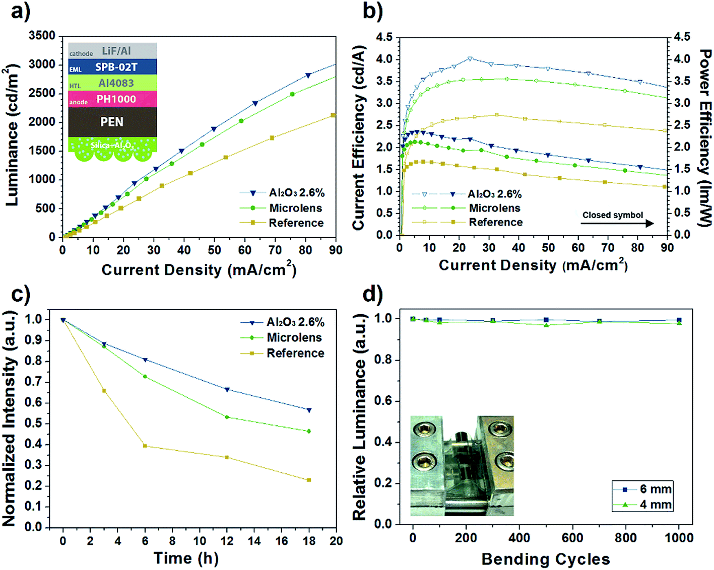 | ||
| Fig. 4 (a) Current density–luminance curves for the devices without a microlens array, with the array, and with the array with embedded Al2O3. Inset shows a schematic illustration of the structure of the flexible, blue light-emitting diode. (b) Current (open symbols) and power (closed symbols) efficiencies versus current density of the devices. (c) Normalized emission intensity of the devices over time. (d) Relative luminance under repeated bending cycles for two different bending radii. The photograph (inset) depicts the bending cycle test. | ||
| Samples | La (cd m−2) | Max. PEa (lm W−1) | Max. CEa (cd A−1) | Rmax.CEa |
|---|---|---|---|---|
| a L: luminance at 20 mA cm−2, max. PE: maximum power efficiency, max. CE: maximum current efficiency, Rmax.CE: relative maximum current efficiency. | ||||
| Reference | 535 | 1.68 | 2.75 | 1 |
| Regular microlens array | 708 | 2.13 | 3.56 | 1.29 |
| Regular microlens array + Al2O3 2.6% | 785 | 2.38 | 4.03 | 1.47 |
| Irregular microlens array | 682 | 2.10 | 3.52 | 1.28 |
| Irregular microlens array + Al2O3 2.6% | 791 | 2.38 | 3.97 | 1.44 |
The microlens array was fabricated opposite to the side where the electrodes, emissive layer, and transporting layers were deposited. Consequently, the current density of the flexible PLEDs remained unchanged regardless of whether the microlens arrays were attached to the substrate (Fig. S3 in ESI†). Because the bare microlens array and that with embedded Al2O3 improved the luminance of flexible PLEDs without changing electrical characteristics, the PLEDs showed higher power and current efficiencies (Fig. 4b). Upon attachment of the array to the PEN substrate, the maximum current efficiency of the PLED increased by 29% relative to that of a bare PEN. Upon mixing of the Al2O3 nanoparticles with the array at 2.6 wt%, the maximum current efficiency of the flexible PLED further increased by 13% relative to that of flexible PLED with the array, and by 47% compared to that of flexible PLED on bare PEN. Therefore, incorporation of Al2O3 nanoparticles in the microlens array is a simple, cost-effective way of increasing the efficiency of the PLEDs.
The normalized luminances over time at 20 mA cm−2 for the flexible blue PLEDs were measured to determine the improvement in stability of the PLED due to gas blocking by Al2O3 nanoparticles in the microlens array. All PLEDs without any encapsulation tended to lose their luminance over a short period under ambient conditions (Fig. 4c). Specifically, the flexible PLEDs degraded rapidly because they were formed on a flexible substrate with poor barrier properties against gas compared with those of glass. In addition, some regions of the emissive layer were directly exposed to ambient air and light because they were not completely covered by a cathode.
Degradation of the exposed emissive polymers could promote the migration of reactive radicals, water, or oxygen gas molecules into nearby unexposed emissive polymers. Hence, the absolute stability of the flexible PLED in this work may be greatly improved simply by changing the processing method such as inkjet printing or selective patterning of emissive layer in order to cover it fully by cathode. Therefore, we simply focused on the relative stability of the flexible PLEDs. Application of the microlens array to the substrate efficiently delayed the degradation of luminance. As a result, relative luminances after they were exposed in ambient air for 18 hours were increased from 0.23 for reference to 0.46 for microlens array, and 0.57 for microlens array with 2.6% Al2O3 nanoparticles. To confirm the enhancement of stability in the flexible PLEDs, water-vapor transmission rates (WVTR) of PEN films were measured (Fig. S4 and S5 in ESI†). The WVTR was reduced from 2.978 g per cm3 per day of bare PEN, to 2.418 and 1.448 g per cm3 per day of PEN coated with silica, and silica with 2.6% of Al2O3 nanoparticles, respectively. Therefore, the improved stability in flexible PLEDs was due to the impeded passage of gas molecules through the silica hybrid film, which consists of organic and inorganic hybrid cross-linked networks.55,56 Degradation of the PLEDs was further slowed by the introduction of Al2O3 nanoparticles in the microlens array. The delayed penetration of the gas molecules may be driven from the blocking of the molecules, not the absorbing them, because the WVTR remained same after the exposure of the samples to the water vapour over 18 h (Fig. S5†). This result indicates that the nanoparticles block the penetration of oxygen and water vapour molecules into the emissive and transporting layers, thereby enhancing stability of the PLED.
The bending test was conducted to confirm the flexibility of the PLEDs. The microlens array showed high flexibility because it consisted of an organic–inorganic hybrid network, therefore the PLED with the array containing Al2O3 also showed high flexibility. When we conducted the bending test at the bending radius of 4 and 6 mm, the luminance of the device stayed at almost same level even after 1000 cycles (Fig. 4d). On the whole, both the efficiency and the stability of the PLEDs were improved using a single layer of the microlens array, and they were fabricated by a simple and cost-effective way. Additionally, the device with the microlens array could be operated in the bent state because of organic–inorganic hybrid network consisting microlens array.
The microlens arrays with Al2O3 nanoparticles were used in a flexible, yellow polymer light-emitting device to determine whether their advantageous effects were not restricted to the blue devices. The device structures are shown in the inset in Fig. S4a.† All of the layers except an emissive layer were retained and the emissive layer was changed to PDY-132, a yellow light-emitting polymer. Fig. S6a in ESI† shows that the luminance of the yellow flexible PLEDs with the microlens array increased from 1265 to 1599 cd m−2 at 20 mA cm−2 (Table S1†); PLEDs with Al2O3 nanoparticles incorporated in the microlens array showed a luminance further increase to 1885 cd m−2. Subsequently, the array improved maximum current efficiency by 24%, and introduction of Al2O3 nanoparticles into the array enhances it more by 12% (Fig. S6b†). A relatively stronger light scattering by Al2O3 nanoparticles at shorter wavelength cause slightly higher enhancement in current efficiency in the blue PLED than yellow PLED. Still, this result suggests that the array PLEDs irrespective of their emission wavelength.
We fabricated an irregular microlens array by a slightly modified method from previous study to reduce optical side effects caused by the microlens array.37 PS particles having diameters of 1 and 1.5 μm were mixed to form a master pattern, and the pattern was transferred to the PEN substrates through the same procedure used to prepare the regular microlens array.
The inset in Fig. 5a displays that PS particles having different diameters were arranged to form somewhat irregular patterns via a simple dip-coating process. The irregular patterns then were transferred to the PEN substrate to form an irregular microlens array (Fig. 5a). Despite of their smaller diameter, 1 μm-sized hemispheres shows light out-coupling efficiency comparable to that of the hemispherical microlenses with 1.5 μm size.45 In addition, inclusion of the smaller hemispheres in the microlens array resulted in a high packing density. Therefore, we expected that the efficiency of the PLED with an irregular microlens array is similar to that of a PLED with a regular microlens array. The structure of device fabricated in this experiment are depicted in an inset of Fig. 5b. We fabricated a SPB-02T-based PLED with an irregular array on a PEN substrate. Irregular microlens arrays were as effective as regular microlens array in enhancing the current efficiency. The maximum current efficiencies achieved with the PLEDs with irregular and regular microlens array increased by 28 and 29%, respectively, compared to a PLED without the array. Incorporation of Al2O3 nanoparticles into the irregular array increased the maximum current efficiency by 44% relative to that of the reference device.
 | ||
| Fig. 5 (a) SEM image of an irregular colloidal array composed of PS particles of 1 and 1.5 μm diameters. Inset shows an SEM image of an irregular microlens array on the PEN substrate. Scale bars are 2 μm. (b) Current efficiency curves for devices with irregular microlens arrays with and without Al2O3 nanoparticles. Inset shows the device structure used in the experiment. (c) Emission spectra of the devices at 20 mA cm−2. Magnified emission spectra at 470–490 nm wavelength range (inset). (d) Angular dependency of the emission from the devices at 20 mA cm−2. | ||
Emission spectra of SPB-02T-based PLEDs with and without microlens arrays are presented in Fig. 5c. Introduction of regular microlens array into a PLED changed the emission spectrum of the PLED relative to that of a reference device. The CIE 1931 colour coordinates for reference device were initially (0.157, 0.205), changing to (0.161, 0.223) upon attachment of a regular microlens array. Even when we incorporated Al2O3 nanoparticles into the array, the emission spectrum of the PLED varied from that of reference device (colour coordinates of (0.160, 0.223)). But when we used an irregular microlens array with the nanoparticles in a PLED, the colour coordinates of the emission spectrum were (0.157, 0.207), which are very close to that of the reference device. As a result, the irregular array minimized the unwanted changes in the emission spectrum of the SPB-02T-based PLED. The refractive angle is directly related to the wavelength of light. When we introduce the irregular microlens array with embedded Al2O3 nanoparticles, the array spreads the light from the PLED in random direction and prevents the light from propagating collectively with specific refractive angles. Therefore, the array can minimize the amplification or offset of the light with specific wavelength. This result coincides with the previous report.37
The viewing-angle dependence of the emissions among PLEDs with and without the microlens arrays are shown in Fig. 5d. Because regular microlens array extracted light entering at a high incident angle with respect to the substrate, the emission intensity at a larger viewing angle for the PLED with a regular array was strong. The radiation pattern became similar to that of the reference device except at 75° upon incorporation of the Al2O3 nanoparticles into the regular microlens array. When we introduce an irregular microlens array with Al2O3 nanoparticles into the PLED, however, the emission patterns at different angles of the PLED became nearly the same as that of reference device. The irregular array with Al2O3 nanoparticles spread light in every direction, thus the radiation patterns became similar to that without the array. These findings suggested that the incorporation of the nanoparticles into the irregular array improved efficiency and stability, as well as minimized the changes in emission spectrum and radiation patterns at different viewing angles.
Conclusions
We demonstrate the simple, cost-effective fabrication of a novel microlens array on a flexible substrate by using a solution process. This array was composed of silica hybrid network with embedded Al2O3 nanoparticles, which were used for their strong light-scattering and gas-blocking abilities. As a result, flexible blue and yellow PLEDs fabricated with the arrays exhibit 47% and 38% enhancement of the maximum current efficiency. Stability of the flexible PLEDs were also enhanced over time by Al2O3 nanoparticles. Furthermore, changes in emission colour and radiation patterns were minimized by incorporation of Al2O3 nanoparticles into the irregular microlens array. In the meantime, they still show efficient light-extraction which results in 44% improvement of maximum current efficiency. Overall, the novel microlens arrays with embedded Al2O3 nanoparticles made in this work efficiently extract light, have high stability and flexibility, as well as minimized changes in optical properties. The novel microlens array helps to take a step forward toward commercial utilization of flexible PLEDs fabricated via all solution processes such as the roll-to-roll process.Acknowledgements
This work was supported by the Climate Change Research Hub of KAIST (grant No. N11160015). Authors want to appreciate Sung Woo Jang for the assistance of the bending test.Notes and references
- C. W. Tang and S. A. Vanslyke, Appl. Phys. Lett., 1987, 51, 913–915 CrossRef CAS.
- J. H. Burroughes, D. D. C. Bradley, A. R. Brown, R. N. Marks, K. Mackay, R. H. Friend, P. L. Burn and A. B. Holmes, Nature, 1990, 347, 539–541 CrossRef CAS.
- M. A. Baldo, D. F. O'Brien, Y. You, A. Shoustikov, S. Sibley, M. E. Thompson and S. R. Forrest, Nature, 1998, 395, 151–154 CrossRef CAS.
- S. Reineke, F. Lindner, G. Schwartz, N. Seidler, K. Walzer, B. Lussem and K. Leo, Nature, 2009, 459, 234–238 CrossRef CAS PubMed.
- H. Sasabe and J. Kido, J. Mater. Chem. C, 2013, 1, 1699–1707 RSC.
- S. H. Wu, M. Aonuma, Q. S. Zhang, S. P. Huang, T. Nakagawa, K. Kuwabara and C. Adachi, J. Mater. Chem. C, 2014, 2, 421–424 RSC.
- T. H. Han, Y. Lee, M. R. Choi, S. H. Woo, S. H. Bae, B. H. Hong, J. H. Ahn and T. W. Lee, Nat. Photonics, 2012, 6, 105–110 CrossRef CAS.
- T. Echigo, S. Naka, H. Okada and H. Onnagawa, Jpn. J. Appl. Phys., 2002, 41, 6219–6222 CrossRef CAS.
- M. Gross, D. C. Muller, H. G. Nothofer, U. Scherf, D. Neher, C. Brauchle and K. Meerholz, Nature, 2000, 405, 661–665 CrossRef CAS PubMed.
- Z. B. Yu, Q. W. Zhang, L. Li, Q. Chen, X. F. Niu, J. Liu and Q. B. Pei, Adv. Mater., 2011, 23, 664–668 CrossRef CAS PubMed.
- M. S. White, M. Kaltenbrunner, E. D. Glowacki, K. Gutnichenko, G. Kettlgruber, I. Graz, S. Aazou, C. Ulbricht, D. A. M. Egbe, M. C. Miron, Z. Major, M. C. Scharber, T. Sekitani, T. Someya, S. Bauer and N. S. Sariciftci, Nat. Photonics, 2013, 7, 811–816 CrossRef CAS.
- T. W. Lee, O. O. Park, L. M. Do and T. Zyung, Synth. Met., 2001, 117, 249–251 CrossRef CAS.
- S. R. Forrest, D. D. C. Bradley and M. E. Thompson, Adv. Mater., 2003, 15, 1043–1048 CrossRef CAS.
- C. Adachi, M. A. Baldo, M. E. Thompson and S. R. Forrest, J. Appl. Phys., 2001, 90, 5048–5051 CrossRef CAS.
- K. Meerholz and D. C. Muller, Adv. Funct. Mater., 2001, 11, 251–253 CrossRef CAS.
- K. Saxena, V. K. Jain and D. S. Mehta, Opt. Mater., 2009, 32, 221–233 CrossRef CAS.
- Z. B. Wang, M. G. Helander, J. Qiu, D. P. Puzzo, M. T. Greiner, Z. M. Hudson, S. Wang, Z. W. Liu and Z. H. Lu, Nat. Photonics, 2011, 5, 753–757 CrossRef CAS.
- T. W. Koh, J. A. Spechler, K. M. Lee, C. B. Arnold and B. P. Rand, ACS Photonics, 2015, 2, 1366–1372 CrossRef CAS.
- M. Zhang, S. Hofle, J. Czolk, A. Mertens and A. Colsmann, Nanoscale, 2015, 7, 20009–20014 RSC.
- Y. Qu, M. Slootsky and S. R. Forrest, Nat. Photonics, 2015, 9, 758–763 CrossRef CAS.
- T. W. Koh, J. M. Choi, S. Lee and S. Yoo, Adv. Mater., 2010, 22, 1849–1853 CrossRef CAS PubMed.
- W. H. Koo, S. M. Jeong, F. Araoka, K. Ishikawa, S. Nishimura, T. Toyooka and H. Takezoe, Nat. Photonics, 2010, 4, 222–226 CAS.
- W. H. Koo, W. Youn, P. F. Zhu, X. H. Li, N. Tansu and F. So, Adv. Funct. Mater., 2012, 22, 3454–3459 CrossRef CAS.
- W. Youn, J. Lee, M. F. Xu, R. Singh and F. So, ACS Appl. Mater. Interfaces, 2015, 7, 8974–8978 CAS.
- W. J. Hyun, J. J. Park, S. H. Im, O. O. Park and B. D. Chin, J. Phys. D: Appl. Phys., 2013, 46, 095107 CrossRef.
- Y. R. Do, Y. C. Kim, Y. W. Song, C. O. Cho, H. Jeon, Y. J. Lee, S. H. Kim and Y. H. Lee, Adv. Mater., 2003, 15, 1214–1218 CrossRef CAS.
- W. J. Hyun, H. K. Lee, S. S. Oh, O. Hess, C. G. Choi, S. H. Im and O. O. Park, Adv. Mater., 2011, 23, 1846–1850 CrossRef CAS PubMed.
- T. Yamasaki, K. Sumioka and T. Tsutsui, Appl. Phys. Lett., 2000, 76, 1243–1245 CrossRef CAS.
- J. J. Shiang, T. J. Faircloth and A. R. Duggal, J. Appl. Phys., 2004, 95, 2889–2895 CrossRef CAS.
- W. J. Hyun, S. H. Im, O. O. Park and B. D. Chin, Org. Electron., 2012, 13, 579–585 CrossRef CAS.
- S. Moller and S. R. Forrest, J. Appl. Phys., 2002, 91, 3324–3327 CrossRef CAS.
- S. H. Eom, E. Wrzesniewski and J. G. Xue, Org. Electron., 2011, 12, 472–476 CrossRef CAS.
- J. M. Park, Z. Q. Gan, W. Y. Leung, R. Liu, Z. Ye, K. Constant, J. Shinar, R. Shinar and K. M. Ho, Opt. Express, 2011, 19, A786–A792 CrossRef CAS PubMed.
- F. Galeotti, W. Mroz, G. Scavia and C. Botta, Org. Electron., 2013, 14, 212–218 CrossRef CAS.
- T. W. Koh, H. Cho, C. Yun and S. Yoo, Org. Electron., 2012, 13, 3145–3153 CrossRef CAS.
- J. H. Hwang, T. H. Park, H. J. Lee, K. B. Choi, Y. W. Park and B. K. Ju, Opt. Lett., 2013, 38, 4182–4185 CrossRef CAS PubMed.
- J. J. Park, W. J. Hyun, K. H. Park, S. H. Im and O. O. Park, Sci. Adv. Mater., 2014, 6, 2370–2377 CrossRef CAS.
- S. T. Ha, O. O. Park and S. H. Im, Macromol. Res., 2010, 18, 935–943 CrossRef CAS.
- H. K. Choi, M. H. Kim, S. H. Im and O. O. Park, Adv. Funct. Mater., 2009, 19, 1594–1600 CrossRef CAS.
- M. Vosgueritchian, D. J. Lipomi and Z. Bao, Adv. Funct. Mater., 2012, 22, 421–428 CrossRef CAS.
- C. S. Deng, H. E. Assender, F. Dinelli, O. V. Kolosov, G. A. D. Briggs, T. Miyamoto and Y. Tsukahara, J. Polym. Sci., Polym. Phys. Ed., 2000, 38, 3151–3162 CrossRef CAS.
- J. Jin, J. J. Lee, B. S. Bae, S. J. Park, S. Yoo and K. Jung, Org. Electron., 2012, 13, 53–57 CrossRef CAS.
- R. K. Bharadwaj, Macromolecules, 2001, 34, 9189–9192 CrossRef CAS.
- B. A. MacDonald, K. Rollins, R. Eveson, K. Rakos, B. A. Rustin and M. Handa, MRS Proceedings, 2003, 769, H9.3 CrossRef.
- Y. Sun and S. R. Forrest, J. Appl. Phys., 2006, 100, 073106 CrossRef.
- G. N. Plass, Appl. Opt., 1964, 3, 867–872 CrossRef CAS.
- E. Kim, H. Cho, K. Kim, T.-W. Koh, J. Chung, J. Lee, Y. Park and S. Yoo, Adv. Mater., 2015, 27, 1624–1631 CrossRef CAS PubMed.
- B. S. Luk'yanchuk, N. V. Voshchinnikov, R. Paniagua-Dominguez and A. I. Kuznetsov, ACS Photonics, 2015, 2, 993–999 CrossRef.
- B. Y. Ouyang, C. W. Chi, F. C. Chen, Q. F. Xi and Y. Yang, Adv. Funct. Mater., 2005, 15, 203–208 CrossRef.
- X. Crispin, F. L. E. Jakobsson, A. Crispin, P. C. M. Grim, P. Andersson, A. Volodin, C. van Haesendonck, M. Van der Auweraer, W. R. Salaneck and M. Berggren, Chem. Mater., 2006, 18, 4354–4360 CrossRef CAS.
- R. Zhu, C. H. Chung, K. C. Cha, W. B. Yang, Y. B. Zheng, H. P. Zhou, T. B. Song, C. C. Chen, P. S. Weiss, G. Li and Y. Yang, ACS Nano, 2011, 5, 9877–9882 CrossRef CAS PubMed.
- W. Gaynor, G. F. Burkhard, M. D. McGehee and P. Peumans, Adv. Mater., 2011, 23, 2905–2910 CrossRef CAS PubMed.
- L. Q. Yang, T. Zhang, H. X. Zhou, S. C. Price, B. J. Wiley and W. You, ACS Appl. Mater. Interfaces, 2011, 3, 4075–4084 CAS.
- H. G. Cheong, R. E. Triambulo, G. H. Lee, I. S. Yi and J. W. Park, ACS Appl. Mater. Interfaces, 2014, 6, 7846–7855 CAS.
- B. Singh, J. Bouchet, G. Rochat, Y. Leterrier, J. A. E. Manson and P. Fayet, Surf. Coat. Technol., 2007, 201, 7107–7114 CrossRef CAS.
- T. Hwang, L. Pu, S. W. Kim, Y. S. Oh and J. D. Nam, J. Membr. Sci., 2009, 345, 90–96 CrossRef CAS.
Footnote |
| † Electronic supplementary information (ESI) available: Photoluminescence spectra of SPB-02T films with and without microlens arrays, voltage–current density curves of blue polymer light-emitting diodes, water vapor transmission rates of the samples, and device characteristic curves for yellow polymer light-emitting diodes with and without microlens arrays. See DOI: 10.1039/c6ra12718e |
| This journal is © The Royal Society of Chemistry 2016 |