
Optical measurement of trace level water vapours using functionalized porous silicon: selectivity studies
Saakshi Dhanekar*ab,
Indu Sharmac and
S. S. Islama
aCentre for Nanoscience and Nanotechnology, Jamia Millia Islamia, (Central University), New Delhi-110025, India. E-mail: sdhanekar@care.iitd.ac.in
bCentre for Applied Research in Electronics (CARE), Indian Institute of Technology (IIT), Hauz Khas, New Delhi-110016, India
cUniversity School of Basic & Applied Sciences, Guru Gobind Singh Indraprastha University, Sector 16-C, Dwarka, New Delhi-110078, India
First published on 22nd July 2016
Abstract
Selective detection of trace level water vapours by functionalized porous silicon (PS) using photoluminescence (PL) quenching technique is reported. This sensitive technique provides sensing data through optical probing on a surface with a submicron surface area. PS samples were prepared via electrochemical etching and were functionalized using ammonium sulphide and UV exposure which brought about major changes in the surface properties. Samples were examined using SEM, FTIR, contact angle and PL spectroscopy. These samples were tested as sensors in the presence of linear aliphatic alcohols and water vapours in the wide range of 0–400 ppm. An increasing trend of sensor response with increase in alcohol chain length and minimal response to water vapours was observed from sensors based on as-anodized PS samples whereas post functionalization, sensors portrayed an opposite response wherein selective response to water vapours and minimal response to alcohols was indicated. The role of surface nitridation is highlighted in selective sensing of water vapours. A correlation between the sensing response and surface chemistry of samples has been established. It is implicated that sensing is directly linked to both the chemical properties of the sensing surface and analytes. A highly sensitive sensor for detection of water vapours at low ppm is presented. A simple and compact design of portable optical sensors, applicable for water vapour sensing is proposed.
1. Introduction
Porous silicon (PS) includes an assembly of a porous matrix with nanocrystallites of silicon. The unique features of this material include a large surface area to volume ratio, high surface reactivity, luminescence at room temperature and ease of compatibility with the electronic industry.1–4 These properties impelled scientists and researchers to use this material in wide application areas of optics and electronic devices such as sensors.5–10Water vapour sensing is an essential requirement in chemical, biomedical, electronics and industry.11,12 There are several materials and methods which have been attempted by researchers for use as water vapour sensors. These have limitations like high temperature processing, high solubility in water and long response- and recovery-time.11–13 Thus, there is requirement of both material and technique which are compatible with current semiconductor industry for ease of device fabrication, processing and packaging. One of the most sensitive optical methods of sensing is photoluminescence (PL) quenching. This phenomena has been so far rarely used by researchers as a sensing tool, where quenching of PL takes place in presence of external analytes.6,14,15 The most peculiar characteristic of this technique is that only a small submicron area equivalent to laser probe region contributes to sensing; therefore, sensing may be correlated to localized morphology, chemical properties of material and nature of analytes vapours (alcohols and water) being sensed. Thus, morphology specified by the submicron probe region plays a key role. There are several reports on functionalization of PS leading to enhancement of PL.16–18 However, selective water vapour sensing using PL quenching technique by surface treated PS at low ppm has not been reported so far. The work being presented here is superior in comparison to documents available on water vapour sensing19–21 due to its smaller probe region, morphology dependency, surface chemistry, high sensitivity at low ppm. Researchers have contemplated to attain long term stability in porous silicon by carbonization,22 chemical treatment,23 thermal treatment24 etc. We have achieved it while functionalizing the PS surface and thus, stability and selectivity were achieved in one step.
In this article, authors have modified the surface chemistry of PS and repeatedly checked its sensing performance and selectivity to water vapour using PL quenching technique. Sensing measurements were recorded in real time and with respect to PL intensity emitted at specific energy. The PL was found to decrease in presence of analytes. Contrary to as-prepared PS samples, functionalized samples had shown maximum response to water vapours and lesser to alcohols. Maximum sensitivity was calculated as 4 unit change/ppm of water vapours. Other sensor parameters like response- and recovery-time were also calculated. Sensors based on functionalized PS samples were found to be highly repeatable and stable in presence of water vapours. Sensing mechanism is interpreted as the change in surface chemistry occurred due to PS surface functionalization. Further, the results were corroborated by SEM, FTIR, contact angle measurements and PL spectroscopy. Sensing response was directly linked to morphology, surface chemistry of PS and chemical properties of analytes.
2. Experimental
Porous silicon (PS) samples were fabricated on silicon substrate, p-type, 〈100〉 orientation, 10 Ω cm resistivity using conventional electrochemical anodization process with current density 30 mA cm−2 for 10 min in a solution of HF (48%) and ethanol in the ratio of 1![[thin space (1/6-em)]](https://www.rsc.org/images/entities/char_2009.gif) :1. The counter electrode used was a platinum mesh and aluminium strip was used for providing backside contact to silicon. The aim was to replace weak and unstable Si–H bonds by more stable bonds Si–N, O–Si–O and HSi(O)3 bonds and also enhance the PL signal. For this purpose, a good surface passivation is required which can be attained by using ammonium sulphide ((NH4)2S). Post anodized samples were subjected to chemical modification by dipping them in a solution of ammonium sulphide ((NH4)2S) and ethanol for around 150 s. These were rinsed in DI water, dried, labelled and few samples were later exposed under UV radiation for 1 and 2 hours. Both short and long UV wavelengths were chosen for optimizing the surface treatment conditions. The samples which were not exposed to UV did not show stable PL and thus were not carried forward for further studies. All samples were stored in vacuum desiccators till tested for sensing. The details of sample specifications are given in Table 1. The sample to be tested was placed in the sensing setup explained elsewhere.6 Sensor measurements were carried out in presence of different analytes like linear aliphatic alcohols (methanol to n-hexanol) and water vapours. The vapours were transported into sensor chamber with the help of carrier gas (nitrogen) with a fixed flow rate of 2 L min−1. The sensor chamber was connected to a computer with Labspec software for data acquisition. The samples were characterized using SEM (Zeiss and Nova NanoSEM), FTIR (Bruker), contact angle measurements (Surface Electro Optics, Model – Phoenix Mini) and PL spectroscopy. PL measurements were taken from Micro-Raman spectrometer (LabRAM HR800 JY) which was fitted with Peltier cooled CCD detector, mapping attachment and an Olympus BX-41 microscope using a 50× LWD microscope objective. The excitation of the samples was performed with an air-cooled Ar+ – laser (Spectra Physics) tuned at 488 nm. The beam was focused at a spot size of 1.19 μm and the power density (∼microwatt per cm2) was kept low to avoid excessive heating in the probe region.
:1. The counter electrode used was a platinum mesh and aluminium strip was used for providing backside contact to silicon. The aim was to replace weak and unstable Si–H bonds by more stable bonds Si–N, O–Si–O and HSi(O)3 bonds and also enhance the PL signal. For this purpose, a good surface passivation is required which can be attained by using ammonium sulphide ((NH4)2S). Post anodized samples were subjected to chemical modification by dipping them in a solution of ammonium sulphide ((NH4)2S) and ethanol for around 150 s. These were rinsed in DI water, dried, labelled and few samples were later exposed under UV radiation for 1 and 2 hours. Both short and long UV wavelengths were chosen for optimizing the surface treatment conditions. The samples which were not exposed to UV did not show stable PL and thus were not carried forward for further studies. All samples were stored in vacuum desiccators till tested for sensing. The details of sample specifications are given in Table 1. The sample to be tested was placed in the sensing setup explained elsewhere.6 Sensor measurements were carried out in presence of different analytes like linear aliphatic alcohols (methanol to n-hexanol) and water vapours. The vapours were transported into sensor chamber with the help of carrier gas (nitrogen) with a fixed flow rate of 2 L min−1. The sensor chamber was connected to a computer with Labspec software for data acquisition. The samples were characterized using SEM (Zeiss and Nova NanoSEM), FTIR (Bruker), contact angle measurements (Surface Electro Optics, Model – Phoenix Mini) and PL spectroscopy. PL measurements were taken from Micro-Raman spectrometer (LabRAM HR800 JY) which was fitted with Peltier cooled CCD detector, mapping attachment and an Olympus BX-41 microscope using a 50× LWD microscope objective. The excitation of the samples was performed with an air-cooled Ar+ – laser (Spectra Physics) tuned at 488 nm. The beam was focused at a spot size of 1.19 μm and the power density (∼microwatt per cm2) was kept low to avoid excessive heating in the probe region.
| S. no. | Sample code | Post anodization processing | ||
|---|---|---|---|---|
| Time for which samples dipped in (NH4)2S (s) | UV exposure wavelength (nm) | UV exposure time (hours) | ||
| 1 | A (as-anodized) | — | — | — |
| 2 | B | 150 | 320 | 01 |
| 3 | C | 150 | 320 | 02 |
| 4 | D | 150 | 260 | 01 |
| 5 | E | 150 | 260 | 02 |
3. Results and discussion
3.1 Surface studies
Fig. 1a(i) depicts the morphology of PS sample. The inset shows a well networked web-like structure containing pores of size nearly 30 nm. Fig. 1a(ii)–(V) display SEM images of functionalized samples exposed to UV radiation. These show an overlay of and agglomeration of (NH4)2S on PS. The morphology of functionalized samples was dependent on the wavelength and exposure time of UV. It can be clearly noted from Fig. 1a(ii) and (iii) that increasing the exposure time of UV with fixed wavelength affects the surface quality and also increases the degree of perturbation. The surface in Fig. 1a(ii) depicts smoothness and that of Fig. 1a(iii) shows disordered pattern. The influence of shorter wavelength on modified PS can be evidenced from Fig. 1a(iv) and (v). The surface as shown in Fig. 1a(iv) is well ordered and structured with pores of size around 1–2 μm. Smaller pores existed within these pores and this is shown in inset of Fig. 1a(iv). With an increase of UV exposure time from 1 to 2 h for shorter wavelength, the sample surface had shown the appearance of irregularly shaped particles and looks disordered and cracked (shown encircled) (Fig. 1a(v)). The SEM images corroborate that surface treatment brings major changes in surface texture of nano-PS. EDX analysis (Fig. 1b) shows the presence of small percentage of oxygen in samples A and smaller percentage of nitrogen and oxygen in samples B–E. In addition to morphology, application of a material as sensor is also linked to surface chemistry; therefore, further studies like FTIR, contact angle measurements and PL spectroscopy were also conducted to understand the surface chemistry. | ||
| Fig. 1 (a) SEM images of samples (i) A, (ii) B, (iii) C, (iv) D, (v) E and (b) EDX analysis of (i) samples A and (ii) samples B–E. | ||
Fig. 2 depicts FTIR of PS (upper part) which shows the presence of 518 cm−1 peak for a site activated by HF and SiH2 vibrations showing peaks at 624, 906 and 2106 cm−1 representing the wag, scissor and stretch modes respectively. A small shoulder peak at 818 cm−1 attributes to Si–O bending band. Silicon has the property to get oxidized quickly and presence of this Si–O is evidencing this fact. FTIR of functionalized PS (lower part of Fig. 2), displays Si–N (837 cm−1), Si–O–Si (1056 cm−1) and HSi(O)3 (2250 cm−1). These peaks were observed to be most intense for samples D and were found to decrease in the order of samples B > samples C > samples E. Samples C and E which were exposed to UV for duration of 2 h depicted FTIR peaks of nearly same order manifesting that irrespective of UV wavelength, long exposure brings about similar chemical effects on the surface.
 | ||
| Fig. 2 FTIR of as-anodized and functionalized PS samples. | ||
Surface treatment shows the presence of surface nitridation and oxidation resulting in the chemical change in surface properties. During chemical reaction, (NH4)2S produces S2− or HS− ions which act as catalyst for formation of HSi(O)3 or Si–O–Si passivation film.16,17
Contact angle measurements were done by sessile-drop method, using a contact angle goniometry. This method describes hydrophobic or hydrophilic nature of the material surface. Contact angle of 115° and 20° was measured for as-anodized and functionalized PS respectively. This confirms that PS was hydrophobic in nature while those functionalized were hydrophilic.
A blue shift as well as considerable change in intensity was noticed in PL for all functionalized PS samples in comparison to as-anodized PS (Fig. 3). The PL peaks for samples A, samples B, samples C, samples D and samples E were positioned in the red region at 1.68 eV, 1.75 eV, 1.74 eV, 1.75 eV and 1.82 eV respectively for in situ study of the quenching phenomenon. The change in intensity and peak shift attributes to the role of luminescence centres. FTIR has shown the PS surface to be covered with silicon hydride bonds, thus hydrides would be the luminescence centres in case of as-anodized PS. In case of functionalized PS, nitrides and oxides could be the possible luminescence centres which could originate from defects and/or impurities contributing to intense and blue shift in PL.
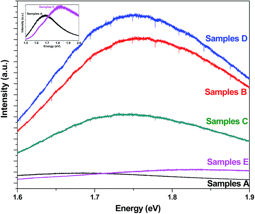 | ||
| Fig. 3 PL of as-anodized and functionalized PS samples. Inset shows the PL spectra of samples A and E separately. | ||
3.2 Sensing studies
Sensing studies were performed at various concentrations of analytes in real time using two methods, (1) recording PL quenching with respect to energy and (2) recording PL peak position quenching with respect to time. | ||
| Fig. 4 (a) PL quenching of samples D sensors in presence of water vapours (0–400 ppm) (b) dynamic response of samples A (blue triangles) and samples D (red squares) sensors in presence of different analytes at fixed concentration of 50 ppm (green dashed lines represent pulse ON/OFF timings for vapours exposure and 50 ppm concentration). While performing PL quenching, the monochromator for samples A and samples D were set at 1.68 eV and 1.75 eV respectively, C1 to C6 indicates the aliphatic chain of alcohol from methanol to n-hexanol (c) dynamic response of functionalized samples to water vapours in the range of 2–100 ppm. The magenta dashed lines represent pulse ON/OFF timings for water vapours exposure and concentration in ppm (d) sensitivity plot for all sensors in presence of alcohols and water vapours; with analyte molecule models where dark grey, light grey and red balls refer to carbon atoms, hydrogen atoms and oxygen atoms respectively. (e) PL quenching repeatability tests for samples D in presence of 50 ppm of water vapours with PL peak position fixed at 1.75 eV. The pink dashed lines represent pulse ON/OFF timings for water vapours exposure and 50 ppm concentration, (f) aging studies of sample D performed in presence of water vapours for a period of 90 days. | ||
This is primarily due to the formation of surface states which act like trap states which forbid the excited electron to drop directly from conduction to valence band. Thus the quenching strength is dependent on both nature of material and quencher molecule. The reason for increasing trend of sensing for alcohol chain can be explained on the basis of vapour pressure and polarity of quenching molecule.26
In the vapour phase, organic molecules with lower vapour pressure tend to get adsorbed on the PS surface. Vapour pressure is governed by boiling point and has an inverse relation. Considering the alcohol chain from methanol to n-hexanol, vapour pressure reduces and thus sensitivity increases. However, increasing trend of sensing response is not noticed beyond n-butanol. This can be explained on the basis of polarity of molecules which also has a significant role. Alcohols have two major sections: one hydrocarbon group and other hydroxyl group. Hydroxyl group has more electron attracting property due to strong electronegativity of oxygen atom. From methanol to n-butanol, hydroxyl group is more dominating than its counterpart while beyond n-butanol, the hydrocarbon group dominates. When quenching takes place, the electrons get trapped which is easier with molecules that tend to show more electron affinity; and thus, strength of quenching increases from methanol to n-butanol and the reverse is noticed beyond n-butanol. Water vapours are not able to quench the PL of samples A due to hydrophobic nature of PS. As-anodized PS surface is covered with hydrides and tends to repel water vapours resulting in less quenching. This is evident from Fig. 4b, upper part.
 | ||
| Fig. 5 Sensing mechanism followed by as-anodized and functionalized samples. | ||
3.3 Sensor packaging
A packaging for testing the sensor on-site is proposed in Fig. 6. It shows the sensor (1) is placed in sealed casing bearing an inlet for analyte vapours (2) and exhaust for venting the sensor packaging. | ||
| Fig. 6 Proposed sensor packaging for on-site testing. | ||
A laser excitation (3) is used for generating the photoluminescence which will be quenched in presence of analytes. With the help of microspectrometer (4), optical intensity will be converted to an electrical signal, which will be sent for signal conditioning and data acquisition. This acquired data can be transferred to a software for data compilation and graphical representation. Such laboratory prototype sensor based on silicon material can easily be integrated with IC industry and can be used as an economical commercial device.
4. Conclusions
A highly sensitive response was obtained from PL quenching of functionalized porous silicon in presence of water vapours. PL helped in inferring the material properties and also served as a powerful sensing tool. As-anodized PS had displayed higher response to alcohols in comparison to water vapours whereas an opposite change was observed when surface was modified. Functionalized PS samples had shown maximum sensitivity to water vapours and a decreasing trend of response to increasing chain length of alcohols. The surface morphology defined by the PL probe played a significant role in sensing. A special emphasis on tunable surface chemistry of PS for water vapours detection at low ppm employing PL quenching has been laid. Ratiocination was made on the basis of results obtained from SEM, FTIR, contact angle measurements, PL spectroscopy and sensing. A contrary behaviour of sensing from functionalized PS surface was imputed to change in material surface morphology, chemistry and nature of analytes (polar/non-polar). High sensitivity and selectivity for water with minimum detection limit of 2 ppm was attained. A packaging design for on-site testing of sensor is also proposed. The data obtained from this study show the viability of integration of such sensors with modern electronics industry for fabrication of smart water vapour sensors.Acknowledgements
Authora is thankful to Department of Science and Technology (DST), Ministry of Science and Technology, Govt. of India for providing financial support through INSPIRE grant no. IFA 12-ENG-13. Authorsa,b would like to acknowledge Ms Sakshi Kapoor, Centre for Nanoscience and Nanotechnology, Jamia Millia Islamia for performing FE-SEM and EDX analysis.References
- M. J. Sailor, Porous Silicon in Practice, 2011, DOI:10.1002/9783527641901.
- O. Bisi, S. Ossicini and L. Pavesi, Surf. Sci. Rep., 2000, 38, 1–126, DOI:10.1016/s0167-5729(99)00012-6.
- H. Föll, M. Christophersen, J. Carstensen and G. Hasse, Mater. Sci. Eng., R, 2002, 39, 93–141, DOI:10.1016/s0927-796x(02)00090-6.
- A. G. Cullis, L. T. Canham and P. D. J. Calcott, J. Appl. Phys., 1997, 82, 909–965, DOI:10.1063/1.366536.
- S. Dhanekar, S. S. Islam, C. M. Julien and A. Mauger, Mater. Des., 2016, 101, 152–159, DOI:10.1016/j.matdes.2016.03.161.
- S. Dhanekar, S. S. Islam and Harsh, Nanotechnology, 2012, 23, 235501, DOI:10.1088/0957-4484/23/23/235501.
- F. A. Harraz, A. A. Ismail, H. Bouzid, S. A. Al-Sayari, A. Al-Hajri and M. S. Al-Assiri, Phys. Status Solidi A, 2015, 212, 1851–1857, DOI:10.1002/pssa.201431780.
- G. Barillaro, Porous Silicon Gas Sensing, in Handbook of Porous Silicon, ed. L. Canham, Springer International Publishing, Switzerland, 2014, pp. 845–856, print ISBN:978-3-319-05743-9 Search PubMed.
- V. Pranculis, R. Karpicz, A. Medvids and V. Gulbinas, Phys. Status Solidi A, 2012, 209, 565–569, DOI:10.1002/pssa.201127309.
- A. G. Nassiopoulou, Porous Silicon for Sensor Applications, in Nanostructured and Advanced Materials for Applications in Sensor, Optoelectronic and Photovoltaic Technology, ed. A. Vaseashta, D. Dimova-Malinovska and J. M. Marshall, Springer, Bulgaria, 2004, pp. 189–204, ISBN: 978-1-4020-3560-9 Search PubMed.
- Z. Chen and C. Lu, Sens. Lett., 2005, 3, 274–295, DOI:10.1166/sl.2005.045.
- B.-H. Wee, W.-H. Khoh, A. K. Sarker, C.-H. Lee and J.-D. Hong, Nanoscale, 2015, 7, 17805–17811, 10.1039/c5nr05726d.
- J. S. Wilson, Sensor Technology Handbook, Elsevier, UK, 2005, DOI:10.1016/j.patrec.2005.01.006.
- P. Kumar and P. Lemmens, RSC Adv., 2015, 5, 91134–91139, 10.1039/c5ra17101f.
- I. Levitsky, Sensors, 2015, 15, 19968–19991, DOI:10.3390/s150819968.
- Z. H. Xiong, L. S. Liao, S. Yuan, Z. R. Yang, X. M. Ding and X. Y. Hou, Thin Solid Films, 2001, 388, 271–276, DOI:10.1016/s0040-6090(00)01887-3.
- M. Lee and H. Tu, Mater. Sci. Semicond. Process., 2007, 10, 276–280, DOI:10.1016/j.mssp.2008.04.001.
- S. Amdouni, M. Rahmani, M. A. Zalbi and M. Oueslati, J. Lumin., 2015, 157, 93–97, DOI:10.1016/j.jlumin.2014.08.041.
- E. Kayahan, Acta Phys. Pol., A, 2015, 127, 1397–1399, DOI:10.12693/Aphyspola.127.1397.
- J. Dian, M. Konečný, G. Broncová, M. Kronďák and I. Matolínová, Int. J. Electrochem. Sci., 2013, 8, 1559–1572 CAS.
- V. Vrkoslav, I. Jelínek, G. Broncová, V. Král and J. Dian, Mater. Sci. Eng., C, 2006, 26, 1072–1076, DOI:10.1016/j.msec.2005.09.025.
- V. Torres-Costa, R. J. Martín-Palma, J. M. Martínez-Duart, J. Salonen and V. P. Lehto, J. Appl. Phys., 2008, 103, 4, DOI:10.1063/1.2910459.
- H. S. Mavi, B. G. Rasheed, A. K. Shukla, R. K. Soni and S. C. Abbi, Mater. Sci. Eng., B, 2003, 97, 239–244, DOI:10.1016/s0921-5107(02)00594-9.
- G. Li, X. Hou, S. Yuan, H. Chen, F. Zhang and H. Fan, J. Appl. Phys., 1996, 80, 5967–5970, DOI:10.1063/1.363593.
- T. Chvojka, V. Vrkoslav, I. Jelínek, J. Jindřich, M. Lorenc and J. Dian, Sens. Actuators, B, 2004, 100, 246–249, DOI:10.1016/j.snb.2003.12.040.
- S. Dhanekar, S. S. Islam, T. Islam and Harsh, Int. J. Nanosci., 2011, 10, 777–781, DOI:10.1142/s0219581x11008885.
- J. M. Lauerhaas and M. J. Sailor, Science, 1993, 261, 1567–1568, DOI:10.1126/science.261.5128.1567.
| This journal is © The Royal Society of Chemistry 2016 |