Jinfeng Liua,
Guisheng Xu*a,
Yanfeng Tianab and
Xiu Zhuab
aKey Laboratory of Transparent Opto-Functional Advanced Inorganic Materials, Shanghai Institute of Ceramics, Chinese Academy of Sciences, 588 Heshuo Road, Shanghai 201899, China. E-mail: gshxu@mail.sic.ac.cn; Fax: +86-21-59927184; Tel: +86-21-69987753
bUniversity of Chinese Academy of Sciences, Beijing 100049, China
First published on 8th June 2016
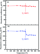
A peculiar temperature-stable piezoelectric performance and strong self-poling effect was observed in tetragonal phase ferroelectric single crystals 0.38Bi(Mg1/2Ti1/2)O3–0.62PbTiO3. The piezoelectric coefficient d33 of the as-prepared sample with self-poling is 158 pC N−1, and it is as high as 75% of the value produced by an external electric field. The internal electric field Ei exists and the value is 4.34 kV cm−1 at the applied electric field of 40 kV cm−1. The defect dipoles pin on the ferroelectric domains and stabilize the piezoelectric properties and the piezoelectric coefficient d33 at room temperature is nearly unchanged until the annealing temperature up to 800 °C, which is much higher than the Curie temperature Tc ∼ 520 °C.
In most cases, the as-prepared unpoled ferroelectrics seldom show a macroscopic polarization, since there are several different polarization states or multi-domains. However, sometimes due to the self-poling, the poled state can set in materials without application of any external electric field. Most of the self-poling phenomena were observed in thin films, such as BiFeO3, Na0.5Bi0.5TiO3, BaTiO3, Pb(Zr, Ti)O3 and Pb(Mg1/3Nb2/3)O3–PbTiO3 based films.8–12 However, in bulk materials, the self-poling phenomena only were reported in a few kinds of materials, such as BiFeO3 ceramics which was treated by a great temperature gradient, Pb(Zr0.35Ti0.65)O3 single crystals with the dimensions of 1 × 1 × 0.2 mm3 and LiNbO3-based single crystals with strong thermoelectric effect.13–15
The reasons for self-poling in different materials are not the same. However, the internal electric field Ei and mechanical forces are the two most important factors. For instance, Chen et al. found an obvious self-poling phenomenon in BiFeO3 ceramics. The high-temperature gradient and corresponding thermal strain caused during the heat treatment process can introduce defect dipoles through separating bismuth vacancies from oxygen vacancies. A mass of these dipoles introduced a macroscopic Ei which poled BiFeO3 ceramics.13 Bdikin et al. observed a self-polarization in Pb(Zr0.35Ti0.65)O3 single crystals via piezoresponse force microscopy (PFM). It was thought that the chemical gradients of lead deficiency near the surface can form a macroscopic Ei which poled the crystals.14 Epitaxial strain can introduce self-poling in some ferroelectric films through the coupling between polarization and strain gradient, i.e. flexoelectricity. Lu et al. demonstrated that the strain gradient generated by the tip of an atomic force microscope can mechanically switch the polarization of a 4.8 nm thickness BaTiO3 epitaxial film on (001) SrTiO3 substrate.10 In addition, in the case of LiNbO3 single crystals the self-poling was caused by the thermoelectric effect and the electric field can be formed by the temperature gradient (Seebeck effect) in the crystals growth process.15
In this investigation, a macroscopic self-poling was observed in 0.38BMT–0.62PT single crystals. The Ei exists and the value is 4.34 kV cm−1 at the applied electric field of 40 kV cm−1. The d33 of the as-prepared sample is 158 pC N−1, which is as high as 75% of the magnitude produced by an external electric field. What's more, it is found that the self-poling is quite stable, and the d33 value nearly keeps the same under various annealing temperatures with the highest temperature up to 800 °C. Thus, due to the self-poling, 0.38BMT–0.62PT crystals may be directly used in some cases without polarization by an external electric field and the piezoelectric properties can self restore at the temperature lower than the Tc if the piezoelectric properties depolarize because of the usage temperature higher than the Tc.
The piezoelectric coefficient d33 of the as-prepared tetragonal 0.38BMT–0.62PT single crystals with (001) orientation is 158 pC N−1, which means that the self-poling exists in the crystals. The d33 of the sample poled by an external electric filed is 208 pC N−1.1 Therefore, the self-poling is very strong and the magnitude of d33 is as high as 75% of the value produced by the external electric field.
The effect of thermal depoling on the values of d33 for the as-prepared 0.38BMT–0.62PT single crystals is demonstrated in Fig. 2(a). It is worth noting that the d33 at room temperature almost keep the same value in the annealing temperature range from 25 °C to 800 °C. Usually a high temperature annealing (above Tc) can result in the complete disappearance of the polarized state or piezoelectric properties in materials with self-poling16 or poled by an external electric filed. However, it is surprisingly found that the value of d33 at room temperature doesn't change even under the heat treatment temperature up to 800 °C, which is much higher than the Tc ∼ 520 °C of the sample. Besides d33, the electromechanical coupling factor k31 is also quite stable as shown in ref. 1. The k31 is about 0.45 at room temperature and it is almost unchanged until the temperature up to the Tc ∼ 520 °C. At the temperature above 520 °C, the k31 of the sample is disappeared.
Fig. 2(b) shows the annealing temperature dependences of the d33 of the sample poled by an external electric filed. It can be seen that the value of d33 at room temperature is nearly unchanged with the annealing temperature increasing from 25 °C to the Tc of the sample. However, when the annealing temperature was higher than the Tc, the value of d33 decreases to about 160 pC N−1, and then it is mainly stable up to 800 °C. By comparison the data between Fig. 1(a) and (b), we can conclude that the d33 of the sample poled by an external electric filed consists of two parts. One part is induced by self-poling, and the other is induced by the external electric filed. When the heat treatment temperature is higher than the Tc, the d33 induced by the external electric filed vanishes, while the d33 induced by self-poling self restores at the temperature below the Tc. As a result, the d33 values of the self-poling sample and the poled sample by an external electric field are nearly the same when the annealing temperature is higher than the Tc. Because the silver electrodes of the sample are easily damaged at the heat treatment temperature above 800 °C, the annealing temperature is not set higher than 800 °C.
![]() | ||
Fig. 3 P–E hysteresis loops of the 0.38BMT–0.62PT single crystals with self-poling measured at 1 Hz as a function of applied electric field. |
Fig. 4 displays the Ec and Ei as a function of applied electric field for the as-prepared sample with self-poling. The magnitude of Ei and coercive field Ec is determined by Ei = (E+ + E−)/2 and Ec = (E+ − E−)/2, where E+ and E− are the intersections of polarization loops with positive and negative field axis, respectively. The value of Ec increases with increasing the applied electric field. There is no tendency of saturation, which may originate from the existence of point defects and electric conductance. The maximum Ei is 4.34 kV cm−1 at the applied electric field of 40 kV cm−1. As the self-polarized state mainly forms during the paraelectric–ferroelectric phase transition around Tc, the Ec of (001) oriented 0.38BMT–0.62PT single crystals at this high temperature is much smaller than that at room temperature and the polarization switching can take place in relatively weak electric field. As a result, it's possible for Ei to be larger than Ec and then to self-pole the as-prepared sample.13
![]() | ||
Fig. 4 Coercive field Ec and internal electric field Ei of the 0.38BMT–0.62PT single crystals with self-poling as a function of applied electric field. |
The internal bias field Ei was usually observed in piezoelectric materials and resulted from the orientation of the defect dipoles.2,17,18 According to the unsaturated P–E loops and large leakage current in the poling process, we can speculate that point defects also exist in 0.38BMT–0.62PT single crystals.
Fig. 5(a) and (b) present the XPS spectra of O 1s of 0.38BMT–0.62PT single crystal before and after sputtering, respectively. For the sputtering sample, the surface of the single crystal was sputtering by argon ion beam about 1 min. Both of the two spectra exhibit a shoulder in the higher binding energy region. The peak at lower binding energy has been attributed to the lattice oxygen in the BMT–PT structure. The other peak at higher binding energy does not follow a regular variation with composition and can be related to the oxygen deficiency.19–21
![]() | ||
Fig. 5 The O1s spectra of 0.38BMT–0.62PT single crystal (a) before sputtering and (b) after sputtering. |
Fig. 6 shows the temperature dependence of dielectric permittivity (εr) for the crystal at 100 Hz and 1000 Hz from room temperature to 710 °C. Two obvious dielectric peaks are observed. The first one at about 520 °C corresponds to the Curie temperature, which was proved by the high temperature XRD of 0.38BMT–0.62PT samples.1,22 The other one is owing to the space charge polarization resulting from oxygen vacancies. The similar phenomena are frequently observed in BMT–PT ceramics.23
![]() | ||
Fig. 6 Temperature dependence of the dielectric permittivity εr of the 0.38BMT–0.62PT single crystals at 100 Hz and 1000 Hz. |
Due to the inevitable volatilization of Bi and Pb during the process of high-temperature single crystals growth, a corresponding amount of and
should form. As a result, the defect dipoles in 0.38BMT–0.62PT single crystals may be
. Because
is the most mobile ionic defect in oxide perovskite, the orientation of the defect dipoles takes place via
diffusion.24 However, the driving force of the diffusion of
in 0.38BMT–0.62PT single crystals is not very clear. We guess that the compositional gradient of point defects such as lead deficiency or bismuth deficiency may be one of the main reasons for the orientation of the defect dipoles in 0.38BMT–0.62PT single crystals, which is similar to the reason for the self-poling in Pb(Zr0.35Ti0.65)O3 single crystals.
With increasing electric field, the shape of P–E exhibits a tendency of changing from asymmetric loops to symmetric ones and the Ei reduces gradually from 4.34 kV cm−1 at 40 kV cm−1 to 2.17 kV cm−1 at 48.5 kV cm−1, which may be caused by the partial realignment of and the defect dipoles relax under higher driving electric field. However, the Ei nearly remains the same value while the applied electric field increases from 48.5 kV cm−1 to 61 kV cm−1. Maybe at the measured frequency 1 Hz, only partial defect dipoles can switch by the external electric field, while the other defect dipoles remain in the original direction due to insufficient time for
to migrate.25 Nevertheless, the Ei may become lower if the applied electric field is much higher or the measured frequency is much lower.
The defect dipoles also related to the good temperature–stable piezoelectric properties. The defect dipoles can pin on the ferroelectric domains, stabilize the domain configuration and reduce domain wall mobility.2,17 So the piezoelectric properties of the (00l) oriented 0.38BMT–0.62PT single crystals are very stable from 25 °C to Tc. At the annealing temperature above the Tc, 0.38BMT–0.62PT single crystal transforms from ferroelectric phase to paraelectric phase. However, in the successive cooling process, because the Ei caused by oriented defect dipoles still exists and repolarizes the sample when the temperature falls below the Tc and the piezoelectric performance self restores almost completely (for unpoled samples) or mostly (for poled samples) as illustrated in Fig. 1. It means that the piezoelectric properties of the actuators and transducers can recover at the temperature lower than the Tc if the piezoelectric properties depolarized because of the usage temperature higher than the Tc. This is very important for the piezoelectric devices used in high temperature environment.
This journal is © The Royal Society of Chemistry 2016 |