Efficient and stable polymer solar cells with electrochemical deposition of CuSCN as an anode interlayer

Ping Fu ab, Xin Guoa, Zhiliang Wangab, Shuwen Yua, Lingyu Zhouab, Wei Yua, Jian Zhangc and Can Li*a
aA State Key Laboratory of Catalysis, Dalian Institute of Chemical Physics, Chinese Academy of Sciences, Dalian National Laboratory for Clean Energy, 457 Zhongshan Road, Dalian 116023, China. E-mail: pfu@dicp.ac.cn
bGraduate University of Chinese Academy of Sciences, Beijing 100049, China
cGuilin University of Electronic Technology, Material Science and Engineering, 1 Jinji Road, Guilin 541004, China

Received 12th May 2016 , Accepted 5th June 2016

First published on 8th June 2016


Abstract

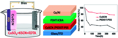
Electrochemical deposition (ECD) of a copper thiocyanate (CuSCN) film as an efficient anode interlayer (AIL) in polymer solar cells (PSCs) is reported. By elaborately optimizing the ECD conditions for the preparation of CuSCN films, a power conversion efficiency (PCE) of 6.16% has been achieved through employing P3HT[thin space (1/6-em)]:[thin space (1/6-em)]IC60BA as the active layer. Concerning the long-term stability, the PSCs with CuSCN as the AIL maintain nearly 84% of their initial PCEs after storing in ambient conditions for 400 hours without any encapsulation, while the PCEs of the reference PSCs with PEDOT:PSS as the AIL largely decrease to 35% of the initial values. Due to the advantages of the high hole mobility and superior chemical stability, ECD-prepared CuSCN is a promising alternative to PEDOT:PSS as the AIL for PSCs.


1. Introduction

Bulk heterojunction (BHJ) polymer solar cells (PSCs) have attracted increasing attention owing to their advantages of low cost, light weight, and feasibility to fabricate flexible devices.1–3 A BHJ PSC is composed of a photoactive layer containing a semiconducting polymer as the donor and a fullerene derivative as the acceptor sandwiched between two electrodes. However, such a simple device configuration suffers from a large energy barrier, severe charge carrier recombination, and remarkable current leakage at the interfaces between electrodes and semiconducting materials, resulting in low device performance. In order to solve this problem, the interlayer inserted between active layer and electrodes is thus widely used.4,5 Desired characteristics of an ideal interlayer include: (1) high transparency across the solar spectrum, (2) appropriate energy levels to form ohmic contact between electrodes and the active layer, (3) suitable wetting properties to facilitate the deposition of active layers, and (4) easy preparation over large-area substrates.

While many efforts have been made on cathode interlayer using materials such as metal oxides, metal carbonates,6–8 titanium chelate9 and polyelectrolytes10–15 for improved device performance, relatively less materials are developed for AIL. To date, poly(3,4-ethylenedioxythiophene):poly(styrenesulfonate) (PEDOT:PSS)16 and metal oxides17–20 are the mostly used AIL materials to increase hole collection in PSCs. However, PEDOT:PSS is not an ideal AIL material due to its chemical instability stemming from intrinsic natures of hygroscopicity and high acidity;21 yet the metal oxides require vacuum deposition and thermal treatment, which is incompatible with the large-scale fabrication and practical application of PSCs. In this regard, it is imperative to develop chemically stable and solution processible alternative AIL materials for enhanced PSC performance.

Recently, copper thiocyanate (CuSCN) has emerged as an promising interfacial material owing to its high hole mobility (≈0.1 cm2 V−1 s−1), excellent transparency in the visible region, and solution processibility. Although some solvents such as dipropylsulfide and diethylsulfide have been adopted to prepare the CuSCN film as AIL for PSCs, perovskite solar cells, light-emitting diodes and field-effect transistors,22–27 the solubility of CuSCN is really limited resulting in the formation of CuSCN film with insufficient uniformity/continuity.28 Moreover, these solvents are toxic and non-ecofriendly. Thus, an electrochemical deposition (ECD) approach in aqueous electrolyte has been used to prepare CuSCN film, which can avoid the use of undesired solvents for solution processing, being compatible with large-area fabrication for flexible substrates. In particular, Chappaz-Gillot et al. have reported on CuSCN thin film or nanowires prepared through ECD method with different electrolytes as AIL for PSC application, in which a PCE of 5.1% was achieved from a PCDTBT/PC70BM-based device.29 However, it should be noting that the CuSCN film quality and morphology are greatly dependent on the ECD conditions including potential, time, as well as temperature, which has been rarely investigated; especially, stability test of devices with CuSCN as AIL which is significant for a PSC application has been never carried out.30,31

Herein, we focus on studying the effect of aforementioned ECD conditions on the CuSCN films as well as the device efficiency and stability of their use as AIL for PSCs. Based on elaborately optimized ECD conditions of CuSCN films, a PCE of 6.16% with Voc = 0.82 V, FF = 0.70, and Jsc = 10.76 mA cm−2 is achieved from the PSC with P3HT[thin space (1/6-em)]:[thin space (1/6-em)]IC60BA as active layer, which is a 17% of improvement in comparison to a reference device using PEDOT:PSS as AIL (Voc = 0.82 V, FF = 0.70, and Jsc = 9.81 mA cm−2, with a PCE of 5.63%). More importantly, CuSCN-based PSCs can maintain 84% of their initial PCEs after storage in ambient conditions for 400 hours, much more stable than devices that based on PEDOT:PSS as AIL, whose PCEs decrease to only 35% under the same conditions. Our results verify that CuSCN is a promising alternative to PEDOT:PSS as the AIL material in PSCs for remarkably improved device stability.

2. Experimental section

Preparation of CuSCN films

The ITO-coated glass substrates (AimCore Technology Co., Ltd) were first sonicated in detergent, acetone, ethyl alcohol, and deionized water in sequence. The CuSCN films were then electro-deposited from an aqueous solution containing 12 mM copper sulphate (CuSO4), 12 mM ethylene diaminetetra acetic acid (EDTA) and 12 mM potassium thiocyanate (KSCN) at a different potential between −0.255 and −0.555 V versus Ag/AgCl (3 M KCl) electrode. After drying with nitrogen flow, the ITO/CuSCN substrates were transferred to N2 filled glove box for device fabrication.

Fabrication and characterization of the PSCs

The P3HT[thin space (1/6-em)]:[thin space (1/6-em)]IC60BA active layers (ca. 160 nm) were spin-casted on top of ITO/CuSCN in a N2 filled glove box from the solution of P3HT[thin space (1/6-em)]:[thin space (1/6-em)]IC60BA (1[thin space (1/6-em)]:[thin space (1/6-em)]1 weight ratio in o-chlorobenzene) with the overall concentration of 25 mg mL−1. Finally 10 nm of Ca and 100 nm of Al were deposited sequentially under 6 × 10⁻⁶ Torr by thermal evaporation through a shadow mask to form an active area of ∼0.064 cm2. In order to ensure the credibility of our results, a batch of device containing 20 cells were fabricated.

The hole mobility test

The structure of hole-only devices is ITO/AILs/MoO3/Au. In the trap-free region over the trap-filled limit, SCLC can be characterized by the Mott–Gurney square law J = (9/8)εrεμh(V2/L3), where ε is the vacuum permittivity, εr is the dielectric permittivity of the active layer, L is the thickness of the AILs, and μh is the hole mobility.

Characterization

The electro-deposition of the CuSCN film was performed on a CHI660 electrochemical workstation (CH Instrument, Inc.). A computer-controlled Keithley 2400 source measure unit was used to characterize the JV performance of devices with an AM1.5 G solar simulator at illumination intensity of 100 mW cm−2. The corresponding incident photon to current conversion efficiency (IPCE) was characterized on the QTest Station 2000ADI system (Crowntech. Inc., USA). The optical transmittance spectra were measured on a Varian Cary 5500 spectrometer. Atomic force microscopy (AFM) height images were obtained using a Bruker Metrology Nanoscope III-D atomic force microscope in tapping mode under atmospheric conditions. The work functions were measured in air by scanning Kelvin probe microscopy (SKPM) with a Bruker Metrology Nanoscope III-D atomic force microscope. Conducting AFM tips (SCM-PIT/PtIr, Bruker, USA) were used for this study with a typical spring constant of 2.8 N m−1 and a resonance frequency of 75 kHz. Typical scan line frequency was 0.3 Hz and each image contained 512 × 512 pixels. The surface potential images were unprocessed original data. Advancing contact angle measurements were performed using a DSA100 system (KRüSS).

3. Results and discussion

The ECD system used in this work is illustrated in Fig. 1(a) (see details in ESI). As an initial study, we examine the crystalline structures of CuSCN films by XRD technique as shown in Fig. 1(b). The XRD patterns of distinct peaks at 2θ = 16.1°, 27.2°, and 30.3° correspond to typical diffractions of (003), (101), and (012) planes, respectively, which indicates the formation of rhombohedral phase (β-phase) in CuSCN films.32 Fig. 1(c) and (d) show device architecture and chemical structures of donor/acceptor materials as well as their energy levels relative to vacuum level. The work function of CuSCN films is slightly higher than PEDOT:PSS, (Fig. S1), which is beneficial for hole extraction and blocking electrons reaching ITO electrode to some extent.
image file: c6ra12355d-f1.tif
Fig. 1 (a) Schematic illustration of the electrochemical deposition method. (b) XRD patterns of the CuSCN film at R.T. (c) Device architecture and chemical structures of P3HT and IC60BA. (d) Energy levels of the materials used in PSCs.

The CuSCN films were prepared under variable deposition potential, time, and deposition temperatures to investigate the effect of ECD conditions on their film morphology. Firstly, the surface morphology of CuSCN films with different deposition potentials (−0.255, −0.355, −0.455, −0.555 V) was examined by atomic force microscopy (AFM). The more negative deposition potential is beneficial for grain refinement leading to homogeneous CuSCN films as shown in Fig. 2, but the deposition potential of −0.555 V may form metal Cu that induce charge carriers recombination based on the device performance described as follows.33 Secondly, the coverage of CuSCN film is obviously time-dependent, hence the deposition time varying from 10 to 40 s was applied at a constant potential of −0.455 V (Fig. S2). When the deposition time is in the range of 20 to 30 s, the ITO substrate can be fully covered with the CuSCN film with a thickness of ca. 40 nm and roughness of 7 nm. Finally, it was found that the morphology of CuSCN films was also ECD temperature dependent (0 °C and R.T.). When depositing at 0 °C, a denser and smoother film can be obtained due to the slow nucleation and growth rate of the CuSCN molecule as shown in Fig. 2(e). In addition, it is worthy of noting that as depicted in Fig. 2(e) and (f) the CuSCN film is more hydrophobic than the PEDOT:PSS film such that the suitable surface energy of CuSCN film would facilitate the deposition of the active layer (Tables S1 and S2).


image file: c6ra12355d-f2.tif
Fig. 2 (a–d) AFM topography images of CuSCN films with different deposition potentials (deposition temperature at R.T.). (e–f) AFM topography images and the surface contact angles of CuSCN (deposition temperature at 0 °C) and PEDOT:PSS films. Scale bar: 5 μm × 5 μm.

The PSCs were fabricated using the CuSCN film prepared under aforementioned optimized conditions as AIL and P3HT[thin space (1/6-em)]:[thin space (1/6-em)]IC60BA as the active layer. The JV curves of these devices under AM1.5 G illumination at 100 mW cm−2 are displayed in Fig. 3(a–d). Detailed characteristic parameters of PSCs are summarized in Table 1. A PCE of 6.16% (Voc = 0.82 V, FF = 0.70, Jsc = 10.76 mA cm−2) employing CuSCN film prepared from the optimized ECD condition (deposition potential of −0.455 V for 30 s at 0 °C) as AIL was achieved, while the PCE of reference device using PEDOT:PSS as AIL can only reach 5.63% (Voc = 0.82 V, FF = 0.70, and Jsc = 9.81 mA cm−2). Obviously, the CuSCN-based device shows better PCE than PEDOT:PSS one due to the increased Jsc. What's more, the better PCE of CuSCN-based device results from the higher Jsc and FF as compared to the best results of the CuSCN nanowire as AIL,29 which might attribute to the denser and smoother CuSCN film with electro-deposited at 0 °C.


image file: c6ra12355d-f3.tif
Fig. 3 JV curves of the PSC with CuSCN as AIL by (a) different deposition potentials; (b) different deposition time; (c) different deposition temperature and (d) JV curves of the PSCs with different AILs. (e) Optical transmission spectra of different AILs. (f) Hole mobility of CuSCN and PEDOT:PSS films measured by SCLC method.
Table 1 Summary of device parameters of the P3HT[thin space (1/6-em)]:[thin space (1/6-em)]IC60BA-based PSCs with CuSCN and PEDOT:PSS as AILs under AM1.5 G illumination (thickness error: ±5 nm)
AIL Varied ECD conditions (thickness) Jsc (mA cm−2) Voc (V) FF (%) PCE (%)
a Data extracted from the literature work.29
CuSCN Potential −0.355 V (45 nm) 9.70 0.82 68 5.44
−0.455 V (45 nm) 9.87 0.82 70 5.67
−0.555 V (45 nm) 9.54 0.80 66 5.04
Time 10 s (25 nm) 10.81 0.76 57 4.71
20 s (35 nm) 10.37 0.80 69 5.76
30 s (40 nm) 10.19 0.82 70 5.86
40 s (50 nm) 10.14 0.80 54 4.38
Temperature R.T. (40 nm) 10.19 0.82 70 5.86
0 °C (40 nm) 10.76 0.82 70 6.16
PEDOT:PSS   (40 nm) 9.81 0.82 70 5.63
CuSCNa   −0.4 V, R.T. (90 nm) 9.60 0.90 59 5.1


The enhanced Jsc can be attributed to the following reasons. Firstly, the transparency of CuSCN is even slightly higher than PEDOT:PSS in the range of 550 nm to 800 nm (Fig. 3(e)), which allows more light to be absorbed by the active layer for generating photocurrents (Fig. S3). Another reason can be the higher hole mobility of CuSCN film than PEDOT:PSS film, which is estimated by the space-charge-limited current (SCLC) model from the hole-only devices (ITO/AILs/MoO3/Au).34 Fig. 3(f) shows the J1/2V curves of the hole-only devices in dark. The hole mobility of CuSCN and PEDOT:PSS are 1.84 × 10⁻⁴ cm2 V−1 s−1 and 8.16 × 10⁻⁵ cm2 V−1 s−1, respectively. The enhanced hole mobility of CuSCN film could further contribute to the enhancement of Jsc. Finally, the reduced series resistance (Rs) and increased parallel resistance (Rsh) with CuSCN as AIL (Rs: 8.2 Ω cm−2, Rsh: 1252.56 Ω cm−2) has been achieved compared to PEDOT:PSS as AIL (Rs: 8.68 Ω cm−2, Rsh: 729.96 Ω cm−2), which might be the formation of better ohmic contact between ITO/CuSCN and active layer.

The incident photon to current conversion efficiency (IPCE) and the integrated current curves of the PSCs with CuSCN and PEDOT:PSS as AILs were measured (Fig. S4). The calculated Jph value by integrating the IPCE spectra is 9.35 mA cm−2 and 8.96 mA cm−2, which are very close to the measured values of the PSCs with CuSCN and PEDOT:PSS as AILs, respectively. The dark JV curves of the PSCs with CuSCN and PEDOT:PSS as AILs exhibit similar reverse saturation and output current, which facilitates the selectivity of the anodes (Fig. S5).35,36 These results demonstrate the potential of CuSCN to replace PEDOT:PSS as AIL for achieving efficient PSCs (Fig. 4).


image file: c6ra12355d-f4.tif
Fig. 4 Lifetime measurements of the non-encapsulated P3HT[thin space (1/6-em)]:[thin space (1/6-em)]IC60BA devices with CuSCN and PEDOT:PSS as AILs under AM1.5 G illumination at 1 sun measured for 400 hours. The curves show the variation in (a) short-circuit current density (Jsc), (b) open-circuit voltage (Voc), (c) fill factor (FF) and (d) PCE and each is normalized to the initial value.

The non-encapsulated devices based on CuSCN and PEDOT:PSS as AILs were tested under AM1.5 G illumination at 1 sun measured for 400 hours in order to study the operational stability of the PSCs. Overall, an initial fast decay in the PCE can be observed within the first 50 h followed by a stable platform. The deterioration of the PCE is in general caused by a decrease in FF and Jsc, whereas the Voc is relatively stable within the measured period. The CuSCN-based PSC exhibits improved stability measured after 400 h, reaching 84% of its initial PCE value, while only 35% of its initial PCE value of the device based on PEDOT:PSS as AIL can maintain. This clearly reveals that the CuSCN-based PSCs provide better stability than the PEDOT:PSS-based counterparts. The poor long-term stability of PEDOT:PSS as AIL can be assigned to its several problems like high acidity and hygroscopicity. In contrast, the CuSCN is more hydrophobic than PEDOT:PSS, which could be manifested by the contact angle test as shown above, favoring the long-term operational stability for the devices. These results provide strong evidences of the general utility of CuSCN as an AIL to be a qualified alternative to PEDOT:PSS for more stable PSCs.

4. Conclusion

In conclusion, we have demonstrated the application of ECD method for the preparation of CuSCN film as AIL for efficient and stable polymer solar cells. PSCs based on CuSCN as AIL was found to increase the Jsc, while maintaining high Voc and FF in comparison with the currently used PEDOT:PSS, hence improving the PSC's maximum PCE to 6.16% by employing P3HT[thin space (1/6-em)]:[thin space (1/6-em)]IC60BA as active layer. More importantly, the device fabricated with hydrophobic CuSCN film as AIL retained 84% PCE after a storage under ambient condition for 400 h without any encapsulation, much more stable than the PEDOT:PSS based PSCs. This work demonstrates that CuSCN is qualified as an effective AIL for efficient and stable PSCs, and meanwhile showing potential application as a stable hole-carrying material for other optoelectronic devices.

Acknowledgements

This work was financially supported by the National Natural Science Foundation of China under Grant No. 21374120 and No. 60377029. X. G. acknowledges the support of the “Thousand Talents Program for Young Scholars” of China.

Notes and references

  1. G. Yu, J. Gao, J. C. Hummelen and A. J. Heeger, Polymer Photovoltaic Cell: Enhanced Efficiencies via a Network of a Internal Donor and Acceptor Heterojunction, Science, 1995, 270, 1789–1795 CAS.
  2. S. Gunes, H. Neugebauer and N. S. Sariciftci, Conjugated Polymer-Based Organic Solar Cells, Chem. Rev., 2007, 107, 1324–1338 CrossRef PubMed.
  3. S. H. Park, A. Roy, S. Beaupre, S. Cho, N. Coates, J. S. Moon, D. Moses, M. Leclerc, K. Lee and A. J. Heeger, Photonics Bulk Heterojunction Solar Cells with Internal Quantum Efficiency Approaching 100%, Nature, 2009, 3, 297 CAS.
  4. J. H. Park, T. W. Lee, B. D. Chin, D. H. Wang and O. O. Park, Roles of Interlayers in Efficient Organic Photovoltaic Devices, Macromol. Rapid Commun., 2010, 31, 2095–2108 CrossRef CAS PubMed.
  5. P. Fu, L. Q. Huang, W. Yu, D. Yang, G. J. Liu, L. Y. Zhou, J. Zhang and C. Li, Efficiency Improved for Inverted Polymer Solar Cells with Electrostatically Self-Assembled Benmelm-Ci Ionic Liquid Layer as Cathode Interface Layer, Nano Energy, 2015, 13, 275–282 CrossRef CAS.
  6. Z. A. Tan, L. J. Li, F. Z. Wang, Q. Xu, S. S. Li, G. Sun, X. H. Tu, X. L. Hou, J. H. Hou and Y. F. Li, Solution-Processed Rhenium Oxide: A Versatile Anode Buffer Layer for High Performance Polymer Solar Cells with Enhanced Light Harvest, Adv. Energy Mater., 2014, 4, 379–386 Search PubMed.
  7. Y. M. Sun, J. H. Seo, C. J. Takacs, J. Seifter and A. J. Heeger, Inverted Polymer Solar Cells Integrated with a Low-Temperature-Annealed Sol–Gel-Derived Zno Film as an Electron Transport Layer, Adv. Mater., 2011, 23, 1679–1685 CrossRef CAS PubMed.
  8. S. Woo, W. H. Kim, H. Kim, Y. Yi, H. K. Lyu and Y. Kim, 8.9% Single-Stack Inverted Polymer Solar Cells with Electron-Rich Polymer Nanolayer-Modified Inorganic Electron-Collecting Buffer Layers, Adv. Energy Mater., 2014, 4, 1356–1361 Search PubMed.
  9. Z. Tan, W. Zhang, Z. Zhang, D. Qian, Y. Huang, J. Hou and Y. Li, High-Performance Inverted Polymer Solar Cells with Solution-Processed Titanium Chelate as Electron-Collecting Layer on Ito Electrode, Adv. Mater., 2012, 24, 1476–1481 CrossRef CAS PubMed.
  10. Z. C. He, C. M. Zhong, S. J. Su, M. Xu, H. B. Wu and Y. Cao, Photonics Enhanced Power-Conversion Efficiency in Polymer Solar Cells Using an Inverted Device Structure, Nature, 2012, 6, 591–595 Search PubMed.
  11. F. Zhang, M. Ceder and O. Inganas, Enhancing the Photovoltage of Polymer Solar Cells by Using a Modified Cathode, Adv. Mater., 2007, 19, 1835–1841 CrossRef CAS.
  12. M. L. Lv, S. S. Li, J. J. Jasieniak, J. H. Hou, J. Zhu, Z. A. Tan, S. E. Watkins, Y. F. Li and X. W. Chen, A Hyperbranched Conjugated Polymer as the Cathode Interlayer for High-Performance Polymer Solar Cells, Adv. Mater., 2013, 25, 6889–6894 CrossRef CAS PubMed.
  13. E. Saracco, B. Bouthinon, J. M. Verilhac, C. Celle, N. Chevalier, D. Mariolle, O. Dhez and J. P. Simonato, Work Function Tuning for High-Performance Solution-Processed Organic Photodetectors with Inverted Structure, Adv. Mater., 2013, 25, 6534–6538 CrossRef CAS PubMed.
  14. C. H. Duan, K. Zhang, C. M. Zhong, F. Huang and Y. Cao, Recent Advances in Water/Alcohol-Soluble Pi-Conjugated Materials: New Materials and Growing Applications in Solar Cells, Chem. Soc. Rev., 2013, 42, 9071–9104 RSC.
  15. F. Huang, H. B. Wu and Y. Cao, Water/Alcohol Soluble Conjugated Polymers as Highly Efficient Electron Transporting/Injection Layer in Optoelectronic Devices, Chem. Soc. Rev., 2010, 39, 2500–2521 RSC.
  16. B. Peng, X. Guo, C. H. Cui, Y. P. Zou, C. Y. Pan and Y. F. Li, Performance Improvement of Polymer Solar Cells by Using a Solvent-Treated Poly(3,4-Ethylenedioxythiophene):Poly(Styrenesulfonate) Buffer Layer, Appl. Phys. Lett., 2011, 98, 243308 CrossRef.
  17. P. Schulz, S. R. Cowan, Z. L. Guan, A. Garcia, D. C. Olson and A. Kahn, Niox/Moo3 Bi-Layers as Efficient Hole Extraction Contacts in Organic Solar Cells, Adv. Funct. Mater., 2014, 24, 701–706 CrossRef CAS.
  18. W. J. Dong, G. H. Jung and J. L. Lee, Solution-Processed-Moo3 Hole Extraction Layer on Oxygen Plasma-Treated Indium Tin Oxide in Organic Photovoltaics, Sol. Energy Mater. Sol. Cells, 2013, 116, 94–101 CrossRef CAS.
  19. K. X. Steirer, P. F. Ndione, N. E. Widjonarko, M. T. Lloyd, J. Meyer, E. L. Ratcliff, A. Kahn, N. R. Armstrong, C. J. Curtis, D. S. Ginley, J. J. Berry and D. C. Olson, Enhanced Efficiency in Plastic Solar Cells Via Energy Matched Solution Processed Niox Interlayers, Adv. Energy Mater., 2011, 1, 813–820 CrossRef CAS.
  20. C. P. Chen, Y. D. Chen and S. C. Chuang, High-Performance and Highly Durable Inverted Organic Photovoltaics Embedding Solution-Processable Vanadium Oxides as an Interfacial Hole-Transporting Layer, Adv. Mater., 2011, 23, 3859–3865 CAS.
  21. M. P. de Jong, L. J. van IJzendoorn and M. J. A. de Voigt, Stability of the Interface between Indium-Tin-Oxide and Poly(3,4-Ethylenedioxythiophene)/Poly (Styrenesulfonate) in Polymer Light-Emitting Diodes, Appl. Phys. Lett., 2000, 77, 2255–2257 CrossRef CAS.
  22. J. W. Jung, C. C. Chueh and A. K. Y. Jen, High-Performance Semitransparent Perovskite Solar Cells with 10% Power Conversion Efficiency and 25% Average Visible Transmittance Based on Transparent Cuscn as the Hole-Transporting Material, Adv. Energy Mater., 2015, 5, 569–575 Search PubMed.
  23. A. Perumal, H. Faber, N. Yaacobi-Gross, P. Pattanasattayavong, C. Burgess, S. Jha, M. A. McLachlan, P. N. Stavrinou, T. D. Anthopoulos and D. D. C. Bradley, High-Efficiency, Solution-Processed, Multilayer Phosphorescent Organic Light-Emitting Diodes with a Copper Thiocyanate Hole-Injection/Hole-Transport Layer, Adv. Mater., 2015, 27, 93–100 CrossRef CAS PubMed.
  24. N. Yaacobi-Gross, N. D. Treat, P. Pattanasattayavong, H. Faber, A. K. Perumal, N. Stingelin, D. D. C. Bradley, P. N. Stavrinou, M. Heeney and T. D. Anthopoulos, High-Efficiency Organic Photovoltaic Cells Based on the Solution-Processable Hole Transporting Interlayer Copper Thiocyanate (Cuscn) as a Replacement for Pedot:Pss, Adv. Energy Mater., 2015, 5, 246–253 Search PubMed.
  25. N. D. Treat, N. Yaacobi-Gross, H. Faber, A. K. Perumal, D. D. C. Bradley, N. Stingelin and T. D. Anthopoulos, Copper Thiocyanate: An Attractive Hole Transport/Extraction Layer for Use in Organic Photovoltaic Cells, Appl. Phys. Lett., 2015, 107, 013301 CrossRef.
  26. K. Zhao, R. Munir, B. Yan, Y. Yang, T. Kim and A. Amassian, Solution-Processed Inorganic Copper(I) Thiocyanate (Cuscn) Hole Transporting Layers for Efficient P-I-N Perovskite Solar Cells, J. Mater. Chem. A, 2015, 3, 20554–20559 CAS.
  27. N. Chaudhary, R. Chaudhary, J. P. Kesari, A. Patra and S. Chand, Copper Thiocyanate (Cuscn): An Efficient Solution-Processable Hole Transporting Layer in Organic Solar Cells, J. Mater. Chem. C, 2015, 3, 11886–11892 RSC.
  28. P. Pattanasattayavong, N. Yaacobi-Gross, K. Zhao, G. O. N. Ndjawa, J. H. Li, F. Yan, B. C. O'Regan, A. Amassian and T. D. Anthopoulos, Hole-Transporting Transistors and Circuits Based on the Transparent Inorganic Semiconductor Copper(I) Thiocyanate (Cuscn) Processed from Solution at Room Temperature, Adv. Mater., 2013, 25, 1504–1509 CrossRef CAS PubMed.
  29. C. Chappaz-Gillot, S. Berson, R. Salazar, B. Lechene, D. Aldakov, V. Delaye, S. Guillerez and V. Ivanova, Polymer Solar Cells with Electrodeposited Cuscn Nanowires as New Efficient Hole Transporting Layer, Sol. Energy Mater. Sol. Cells, 2014, 120, 163–167 CrossRef CAS.
  30. Y. Ni, Z. G. Jin and Y. Fu, Electrodeposition of P-Type Cuscn Thin Films by a New Aqueous Electrolyte with Triethanolamine Chelation, J. Am. Ceram. Soc., 2007, 90, 2966–2973 CrossRef CAS.
  31. S. Y. Ye, W. H. Sun, Y. L. Li, W. B. Yan, H. T. Peng, Z. Q. Bian, Z. W. Liu and C. H. Huang, Cuscn-Based Inverted Planar Perovskite Solar Cell with an Average Pce of 15.6%, Nano Lett., 2015, 15, 3723–3728 CrossRef CAS PubMed.
  32. T. Iwamoto, Y. Ogawa, L. N. Sun, M. S. White, E. D. Glowacki, M. C. Scharber, N. S. Sariciftci, K. Manseki, T. Sugiura and T. Yoshida, Electrochemical Self-Assembly of Nanostructured Cuscn/Rhodamine B Hybrid Thin Film and Its Dye-Sensitized Photocathodic Properties, J. Phys. Chem. C, 2014, 118, 16581–16590 CAS.
  33. W. Wu and J. Qiu, Characteristics of p CuSCNthin film prepared by electrochemicaldeposition, J. Chin. Ceram. Soc., 2004, 32, 1088–1093 CAS.
  34. A. M. Goodman, Double Extraction of Uniformly Generated Electron-Hole Pairs from Insulators with Noninjecting Contacts, J. Appl. Phys., 1971, 42, 2823 CrossRef CAS.
  35. T. B. Yang, M. Wang, C. H. Duan, X. W. Hu, L. Huang, J. B. Peng, F. Huang and X. Gong, Inverted Polymer Solar Cells with 8.4% Efficiency by Conjugated Polyelectrolyte, Energy Environ. Sci., 2012, 5, 8208–8214 CAS.
  36. K. Zhang, C. M. Zhong, S. J. Liu, C. Mu, Z. K. Li, H. Yan, F. Huang and Y. Cao, Highly Efficient Inverted Polymer Solar Cells Based on a Cross-Linkable Water-/Alcohol-Soluble Conjugated Polymer Interlayer, ACS Appl. Mater. Interfaces, 2014, 6, 10429–10435 CAS.

Footnotes

Electronic supplementary information (ESI) available. See DOI: 10.1039/c6ra12355d
Ping Fu and Xin Guo contributed equally to this work.

This journal is © The Royal Society of Chemistry 2016