
 Open Access Article
 This Open Access Article is licensed under a Creative Commons Attribution-Non Commercial 3.0 Unported Licence
Catalyst-free site-specific surface modifications of nanocrystalline diamond films via microchannel cantilever spotting†
Marina
Davydova
*a,
Andres
de los Santos Pereira
b,
Michael
Bruns
c,
Alexander
Kromka
a,
Egor
Ukraintsev
a,
Michael
Hirtz
d and
Cesar
Rodriguez-Emmenegger
*be
aInstitute of Physics v.v.i., Academy of Sciences of the Czech Republic, Cukrovarnicka 10, 16200 Prague 6, Czech Republic. E-mail: davydova@fzu.cz
bDepartment of Chemistry and Physics of Surfaces and Biointerfaces, Institute of Macromolecular Chemistry v.v.i., Academy of Sciences of the Czech Republic, Heyrovsky Sq. 2, 16206 Prague 6, Czech Republic
cInstitute for Applied Materials (IAM), Karlsruhe Nano Micro Facility (KNMF), Karlsruhe Institute of Technology (KIT), 76344, Eggenstein-Leopoldshafen, Germany
dInstitute of Nanotechnology (INT), Karlsruhe Nano Micro Facility (KNMF), Karlsruhe Institute of Technology (KIT), 76344, Eggenstein-Leopoldshafen, Germany
eDWI – Leibniz Institute for Interactive Materials and Institute of Technical and Macromolecular Chemistry, RWTH Aachen University, Forckenbeckstraße 50, 52074 Aachen, Germany. E-mail: rodriguez@dwi.rwth-aachen.de
First published on 8th June 2016
Abstract
The properties of nanocrystalline diamond (NCD) films offer great potential for the creation of various sensing and photonic devices. A great challenge in order to materialize such applications lies in achieving the micrometrically resolved functionalization of NCD surfaces. In the present work, we introduce a facile approach to meet this challenge employing the novel strain-promoted alkyne–azide cycloaddition “click” chemistry reaction, a catalyst-free ligation protocol compatible with biomolecules. The ability to achieve well-resolved multicomponent patterns with high reproducibility is demonstrated, paving the way for the fabrication of novel devices based on micropatterned NCD films.
1 Introduction
Besides being the hardest of all materials, diamond occupies a special place in industry. Its electronic properties, including a 5.47 eV band gap, make diamond a promising semiconductor material. Currently, diamond can be prepared synthetically either as a bulk material under high pressure and high temperature or in the form of thin films by chemical vapor deposition (CVD). The surface electronic properties of intrinsic diamond can be significantly altered by contact with oxidative or reductive plasma. Diamond hydrogen or oxygen surface termination results in marked differences in properties such as electrical conductivity, electron affinity, and surface wettability.1 Bulk doping with boron (p-type) and nitrogen or phosphorous (n-type) can also be incorporated during the thin film deposition process to tune the semiconductor properties.2,3Microwave CVD has become the preferred deposition technique for opto-electronic applications due to its advantages, including large area deposition, high growth rate, and high surface quality. This technique usually yields films composed of nanocrystals, termed nanocrystalline diamond (NCD). Their inexpensive production on a large variety of substrates of arbitrary size and shape compared to monocrystalline diamond makes NCD films a more feasible alternative for industrial applications.4,5
Recently, NCD films have been utilized for advanced electronic devices in the field of sensing, including gas sensors and photonic devices, as well as biosensors.6–9 As an example, hydrogen-terminated NCD films have been shown to exhibit changes in their surface conductivity in the presence of phosgene and could be utilized as a physical transducer to detect this gas.10 In a similar fashion, the amperometric detection of glucose was accomplished by the immobilization of glucose oxidase enzyme on NCD films.11
Generally, diamond-based sensing devices rely on the binding and reaction of molecules directly at the NCD surface.12,13 In the vast majority of cases, the specificity of the sensor response depends on the presence of appropriate receptors immobilized onto the surface.9 Thus, in order to extend the applications of NCD films in the field of sensing, as well as biotechnology, the ability to functionalize their surface is a prerequisite.9 In particular, being able to encode different functionalities in precise regions of NCD films can be envisioned as a feasible route for the design of surfaces with controlled interactions in biological environments,14,15 as well as high-throughput sensors.
Surface immobilization of bioactive molecules by spotting and printing methods has drawn much attention in recent years, as it is a base technique for the preparation of structured, bioactive surfaces.16–19 For highest feature resolution in the nanoscale, techniques like dip-pen nanolithography (DPN) and polymer pen lithography (PPL) offer interesting lithography routes.16,20 While ink jet printing offers contactless high-throughput spotting at larger length scales (usually >50 μm), techniques as microcontact printing (μCP) and spotting with microchannel cantilevers (μCS)21 can readily address the scale range down to a few microns.18,22 The deposition of micro-reactors on a surface to allow liquid phase coupling chemistry to take place for prolonged time or transfer of otherwise not writable species is used in DPN and PPL in the form of matrix-assisted transfer (MA-DPN/MA-PPL).23 Similarly, μCS was previously demonstrated for the spotting of femtoliter–scale reaction chambers for surface immobilization of bioactive substances into microarrays by “click” chemistry.24,25 The click reaction chosen in the previously mentioned approaches is the copper-catalyzed alkyne–azide cycloaddition (CuAAC), that has proven enormously useful for biochemical coupling reactions since the introduction of the concept by Sharpless.26,27 In particular, several examples have been reported in which the CuAAC reaction was employed to functionalize the surface of diamond materials, including nanoparticles,28 detonation diamond nanoparticles,29 or conductive diamond,30–34 which provided an avenue to electrochemically stable, functional electrodes.
However, since terminal alkynes are rather unreactive towards azides, the efficiency of the CuAAC reaction strictly relies on the presence of a Cu(I) catalyst species, often achieved by combining CuSO4 with sodium ascorbate. This requirement poses a serious drawback for several applications.35 In the electronic fields the presence of Cu-ions on the surface can disrupt monolayer conductivity.36 Particularly in many applications in the biological field, the presence of such ions cannot be tolerated, as they are cytotoxic and can disrupt the conformation of the biomacromolecules to be patterned, including proteins and DNA.37,38 Though extensive washing or the use of heterogeneous catalysis can often alleviate the problem, concerns about the need for Cu-ions remain.39
In order to overcome these limitations altogether, reactions are sought which proceed rapidly at room temperature, in aqueous solvents, and do not require any catalyst. In this regard the copper-free strain-promoted alkyne–azide cycloaddition (SPAAC) click reaction, developed by Bertozzi and coworkers, has attracted considerable attention.35,40 It relies on the use of strained cyclooctynes and their derivatives to activate the reactions. Thus, reaction rates are very fast without the need for a metal catalyst. Its bioorthogonality and compatibility with biological molecules has been thoroughly demonstrated, as the reaction could even be applied to in vivo labeling and imaging.40,41
Importantly, SPAAC reactions have been found to be suitable for the functionalization of material surfaces such as silicon, gold, or glass but also quantum dots, nanoparticles and polymer nanofibers.42,43 Silane chemistry was used by Popik and coworkers to mediate the covalent surface attachment of the strained alkyne to glass slides, after which the SPAAC reaction was carried out in a surface-confined fashion.44 A further refinement of this strategy consisted in the surface grafting of functionalizable polymer brushes and their side-chain substitution with “masked” dibenzocyclooctynes (DBCO), which could be converted to the strained alkyne form by irradiation with UV-light, allowing the ensuing SPAAC reaction to take place in a spatially resolved manner.45 A later approach used microcontact printing in order to achieve the patterning.46 Postpolymerization-functionalized surface-grafted polymer brushes were also used to compare the reaction kinetics of two types of DBCO-derivatives with an azide.47
On the other hand, the surface immobilization of azide groups followed by SPAAC reaction with a cyclic alkyne present in solution has also been exploited.48 Various surface functionalization strategies based on SPAAC have been reviewed recently.49 The advantages of this novel catalyst-free click reaction can be therefore envisioned to further expand the power of μCS, PPL, and DPN.
Herein, we demonstrate a facile route for the surface functionalization of NCD films via μCS in order to create small-scale patterns suitable for different types of sensor applications. For this purpose, we create functionalized silane coatings bearing chemical groups that can participate in either the established CuAAC reaction or the catalyst-free SPAAC reaction. Moreover, we compare the effectiveness of both protocols for μCS. We further assess the possibility of employing this method to create well-resolved multi-component patterns on the NCD film surface.
2 Experimental
2.1 Materials
(3-Glycidyloxypropyl)trimethoxysilane (98%), dibenzocyclooctyne-amine (DBCO), and propargylamine were purchased from Sigma-Aldrich (Czech Republic). Silicon wafers used as the substrate for nanocrystalline diamond film deposition were acquired from Siegert Wafer GmbH (Aachen, Germany). The fluorescent inks tetramethylrhodamine (TAMRA) azide, Alexa fluor 488-azide, Cy5-azide, CuSO4 and ascorbic acid were acquired from Sigma-Aldrich (Germany). (3-Glycidyloxypropyl)trimethoxysilane was purified by vacuum distillation.2.2 Methods
2.2.1.1 Deposition of nanocrystalline diamond films. The deposition of nanocrystalline diamond film on the silicon substrates proceeded in two steps: (i) seeding for 40 min, and (ii) microwave plasma-enhanced chemical vapor deposition (PECVD). Prior to the diamond deposition, the substrates were ultrasonically cleaned in isopropyl alcohol and afterwards rinsed with deionized water. Then, the substrates were immersed for 40 min into an ultrasonic bath containing an ultra-dispersed diamond colloidal suspension. This process leads to the formation of a 5 to 25 nm thin layer of nanodiamond powder on the Si substrate. The nucleation procedure was followed by the microwave PECVD using a pulsed-linear antenna microwave chemical plasma system (Roth&Rau AK 400).4 The deposition of the NCD layer was carried out using a microwave power of 2 × 1700 W, pressure of 0.1 mbar, with a gas mixture of H2, CH4 and CO2 (100/5/30 sccm) and substrate temperature of 500 °C.
2.2.1.2 Self-assembled monolayer (SAM) of epoxide. The substrates coated with a deposited NCD layer were rinsed twice with ethanol and deionized water, dried by blowing with nitrogen, and exposed to air plasma for 20 min. Subsequently they were immersed in a 1% (v/v) solution for (3-glycidyloxypropyl)trimethoxysilane in dry toluene and kept for 8 h at room temperature in a dry environment. After this time, the samples were removed from the solution, rinsed with toluene and acetone and dried by blowing with nitrogen.
2.2.1.3 Immobilization of the clickable group. Immediately after silanization, the samples were immersed in a solution of either propargylamine 2% (v/v) or dibenzocyclooctyne-amine (DBCO, 1 mg mL−1) in dry dichloromethane in individual sealed vials. The reaction was allowed to proceed at 35 °C for 12 h. Subsequently, the samples were rinsed with dichloromethane, acetone, ethanol, and water, and dried by blowing with nitrogen.
2.2.2.1 Dye solutions used for patterning. All fluorescent dye solutions used in this work in the μCS procedure (“inks”) consisted of either TAMRA-azide, Alexa fluor 488-azide, or Cy5-azide, in all cases at a concentration of 100 μg mL−1, dissolved in a mixture of water/glycerol (7
![[thin space (1/6-em)]](https://www.rsc.org/images/entities/char_2009.gif) :3) to prevent drying. For the solutions to be patterned on propargyl-functional NCD films via CuAAC, CuSO4 (10 mM) and sodium ascorbate (20 mM) were added as catalyst. In the case of the dye solutions patterned on DBCO-functional NCD films using the SPAAC reaction, no catalyst was added.
:3) to prevent drying. For the solutions to be patterned on propargyl-functional NCD films via CuAAC, CuSO4 (10 mM) and sodium ascorbate (20 mM) were added as catalyst. In the case of the dye solutions patterned on DBCO-functional NCD films using the SPAAC reaction, no catalyst was added.
2.2.2.2 Pattern writing via μCS. All patterns were written with an NLP 2000 system (NanoInk, USA) using on-board software (NanoInk, USA) that allows programming of the dwell time and position of the surface patterning tool (SPT-S-C10S, Bioforce Nanosciences). Prior to use, the SPT pens were plasma cleaned by oxygen plasma (10 sccm O2, 100 mTorr, 30 W for 5 min). Then, the SPT was mounted onto the tip holder by double-sided sticky tape and the pen reservoir was filled with 1 μL of the corresponding dye solution. The spotting proceeded at a relative humidity of 60% and with the sample stage titled by 8° with respect to the tip. For all patterns, a dwell time of 0.5 s was used. After the lithography process, the click reaction between surface and azide-functional dye (either CuAAC or SPAAC) was allowed to proceed for 1 h in dark at a constant humidity of 60%. Subsequently, the samples were rinsed with ethanol and deionized water to remove the excess solution, and dried by blowing with nitrogen.
2.2.3.1 Scanning electron microscopy (SEM). The morphology of the nanocrystalline diamond films was obtained by scanning electron microscopy (SEM, Raith e_LiNE). The images were taken at accelerating voltages of the primary electrons of 10 kV and in-lens detector was used.
2.2.3.2 Fluorescence microscopy. Fluorescence microscopy images were taken with a Nikon upright fluorescence microscope (Eclipse 80i), equipped with a sensitive camera CoolSNAP HQ2 (Photometrics). The broadband excitation light source (Intensilight illumination) is combined with sets of filters (Texas Red, FITC, DAPI) to separate excitation and emission spectra, depending on the used dye molecule. The fluorescence image analysis for determination of spot area was done in ImageJ software by applying a threshold to the raw images and using the particle analysis tool.50
2.2.3.3 Atomic force microscopy (AFM). The surface topography of the NCD films was characterized in quantitative nanomechanical mapping mode of PeakForce AFM system (ICON, Bruker) using new Multi75AL cantilever treated in CF4 plasma (pressure 100 mTorr) for 30 s. The root-mean-square roughness (RRMS) was evaluated from two scan area sizes: 5 × 5 μm2 and 1 × 1 μm2.
2.2.3.4 Raman spectroscopy. Micro-Raman spectroscopy (InVia Reflex by Renishaw) using a HeCd laser with a 442 nm excitation wavelength, and spot diameter 2 μm was employed to assess the allotropic components of the NCD films.
2.2.3.5 Thickness measurement. The thickness of the NCD films was evaluated from the interference fringes of the reflectance spectra measured in UV-vis-NIR region using a custom-made device and commercial software for modelling the optical properties of the thin film.
2.2.3.6 X-ray photoelectron spectroscopy (XPS). A K-Alpha spectrometer (Thermo Fisher Scientific, East Grinstead, UK) was used to perform XPS measurements. The samples were analyzed using a micro-focused, monochromated Al Kα X-ray source (400 μm spot size). The kinetic energy of the electrons was measured using a 180° hemispherical energy analyzer operated in the constant analyzer energy mode (CAE) at 50 eV pass energy for elemental spectra. Thermo Avantage software was used to analyze the spectra. The spectra were fitted with one or more Voigt profiles (binding energy uncertainty: ±0.2 eV). The analyzer transmission function, Scofield sensitivity factors,51 and effective attenuation lengths (EALs) for photoelectrons were applied for quantification. EALs were calculated using the standard TPP-2M formalism.52 All spectra were referenced to the C 1s peak of hydrocarbons at 285.0 eV binding energy controlled by means of the well-known photoelectron peaks of metallic Cu, Ag, and Au.
3 Results and discussion
In this study, we report a new approach for the surface functionalization of NCD films via μCS using alkyne–azide cycloaddition click reactions with the purpose of creating small-scale patterns (Fig. 1).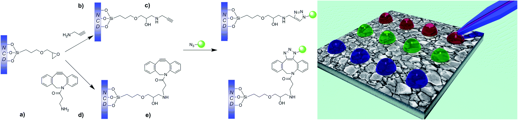 | ||
| Fig. 1 Schematic representation of the chemical strategy used for the functionalization of NCD films: (a) silanization with (3-glycidyloxypropyl)trimethoxysilane, (b) ring-opening of the epoxide group with propalgylamine to yield an amino alcohol, (c) CuAAC click chemistry reaction of immobilized propargyl groups with incoming azide, (d) ring-opening of the epoxide group with dibenzocyclooctyne-amine (DBCO), and (e) Cu- free SPAAC click chemistry reaction of immobilized DBCO groups with incoming azide. | ||
3.1 Deposition of nanocrystalline diamond films
The growth of NCD films on silicon wafer substrates was carried out using a plasma-enhanced CVD method. The thickness of the pristine NCD layers was measured by the spectral reflectance method assessing the interference fringes and was found to be 448 nm. Further characterization of the NCD layers was carried out by scanning electron microscopy (SEM), Raman spectroscopy, and atomic force microscopy (AFM). SEM image (Fig. 2a) clearly indicates the polycrystalline nature of a continuous film consisting of grains in sizes up to 200 nm. Moreover, a SEM micrograph of the cross-section of the layer (ESI, Fig. S1†) supports the homogeneity of the NCD layer thickness, providing a value of (435 ± 13) nm, which corresponds well with the measurement by optical means. The topography of the film, as assessed by AFM, also reveals a uniform and homogeneous coverage of the Si substrate with the diamond film (Fig. 2c). The surface roughness (RRMS) was evaluated from 5 × 5 μm2 and 1 × 1 μm2 scanned areas and was determined to be (16 ± 2) nm. This relatively low value of RRMS in comparison to other NCD growth methods (typically between 30 and 50 nm for NCD films)53 is an important feature for many areas of application. It is noteworthy that the roughness can be tuned by varying the deposition parameters such as temperature, gas flow rate, and pressure, as was shown in previous reports.54 For instance, it has been reported that the pressure has a sharp influence on the deposition process, as it can lead to inhibition of the film growth.4 Increasing the partial pressure of oxygen in the precursor gases either as a pure O2 or in the form of CO or CO2 has been described for the purpose of enhancing the growth rate and improving the diamond film quality.55,56 Moreover, the partial pressure of hydrogen in the feed gas plays an important role in determining the morphology of the film. Its decrease was reported to lead to a change the morphology from discrete well-faceted diamond grains larger than 100 nm to finer granular structures with sizes in the order of 30 nm.57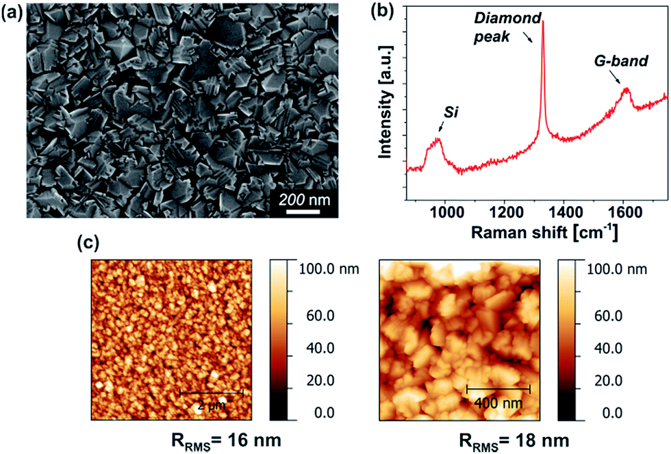 | ||
| Fig. 2 SEM image of pristine NCD film (a), Raman spectrum of NCD film (b). The sharp peak at 1330 cm−1 proves the diamond character of the deposited films. AFM topography images of NCD film (c). | ||
The Raman spectrum (Fig. 2b) is characterized by three strong contributions. The peak centered at 970 cm−1 (Si-peak) reflects the second-order peak of the Si substrate.58 The Raman peak centered at 1330 cm−1 corresponds to the diamond (sp3-bonding) component. The broad band at approximately 1610 cm−1 is attributed to the non-diamond phase (G-band), i.e., sp2-bonded carbon atoms.4 The high intensity of the diamond peak with respect to the G-band indicates a strong predominance of the diamond phase in the film with respect to the graphite component.
3.2 Modification of NCD films with reactive coatings for μCS
In order to allow for a rapid and well-defined functionalization of the prepared NCD films using μCS, the surfaces were coated with a siloxane layer containing two types of chemical groups able to undergo a click chemistry reaction in the presence of an azide-containing molecule. The versatility of silane chemistry has enabled its utilization for a variety of nanoapplications. These range from the silica coating of iron particles to the surface modification of carbon nanofibers for polymer nanocomposites.59–61 The preparation of these clickable layers proceeded in two steps: (1) immobilization of a silane containing an epoxide ring, and (2) nucleophilic epoxide opening with a primary amine bound to the clickable group (Fig. 1). While the silane immobilization step was common for both types of layers prepared, the nature of the clickable group immobilized could be changed simply by selecting an appropriate primary amine.The successful preparation of the targeted layers was confirmed by means of XPS. Fig. 3 shows the changes recorded in the Si 2p and N 1s regions of the spectra after the successive reaction steps. The Si 2p region in particular confirms the attachment of the siloxane layer by the appearance of two signals.62 They arise from the Si atoms in the layer bonded to different oxygen-containing surface groups and to each other by siloxane bonds. Their binding energies are observed at 101.5 eV and 102.8 eV, and indicate that the Si atoms are bonded to between 1 and 3 oxygen atoms.63,64 The signals are broadened by splitting into closely spaced 2p3/2 and 2p1/2 components due to spin–orbit coupling, which are not individually resolved.
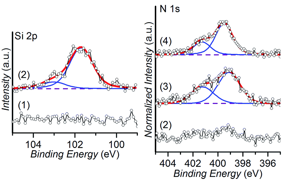 | ||
| Fig. 3 XPS spectra of the Si 2p (left) and N 1s (right) regions, showing the differences between the bare NCD surface (1), epoxide silane surface (2), propargyl-functionalized NCD (3), and DBCO-functionalized NCD (4). | ||
Propargylamine was chosen to prepare the surface to be functionalized using CuAAC. In our previous work we have demonstrated the effectiveness of this strategy for the surface functionalization of model substrates using DPN.65 However, in order to overcome the requirement for a transition metal catalyst in the DPN ink formulation, we introduced a surface capable of participating in the SPAAC click reaction. While the CuAAC has enabled great advances in surface functionalization in general, and in particular for DPN and μCS, the use of a Cu-based catalyst may pose severe limitations for the patterning of some types of biomolecules whose activity may be impaired. Two main strategies have been introduced to increase the reactivity of the alkyne group in order to enable the cycloaddition reaction with an azide to proceed without catalyst, involving the activation of the triple bond with fluorine electron-withdrawing groups or placing it in a strained cycle.66 In particular, dibenzocyclooctynes (DBCOs) show significantly increased reaction rates with azides, which allow for the strain-promoted alkyne–azide cycloaddition to proceed in absence of any Cu-species.67 Thus, a DBCO-presenting a primary amine group was chosen in this work for the nucleophilic attack to the epoxide ring (Fig. 1). The binding of both types of amines to the surface is observed in the XPS spectra of the N 1s region, where signals are observed corresponding to C–N/O![[double bond, length as m-dash]](https://www.rsc.org/images/entities/char_e001.gif) C–N groups (399.5 eV) and to partially protonated amino groups (401.3 eV),62,68 in contrast to the non-reacted epoxide surface (Fig. 3).
C–N groups (399.5 eV) and to partially protonated amino groups (401.3 eV),62,68 in contrast to the non-reacted epoxide surface (Fig. 3).
3.3 Pattern fabrication via μCS and comparison of reactions
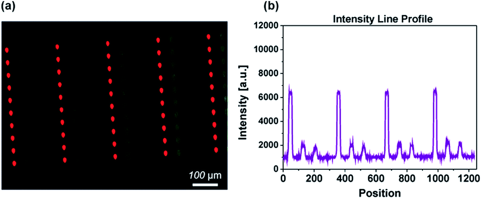
The ability to create microarrays on the NCD films modified with “clickable” coatings was demonstrated using μCS. This was achieved by spotting the ink with an SPT attached to a DPN platform where the sample stage can be moved with high precision in all three directions (x, y and z).21 The spotting process was relatively fast as it can yield an area of 500 × 500 μm2 with 100 dots in about 2 min.69Firstly, we compared two different types of click chemistry reactions, i.e. CuAAC and Cu-free SPAAC click reactions, by performing μCS with a fluorescent azide-containing molecule on the NCD films modified with either propargyl or DBCO reactive groups. It should be noted that in both cases after the lithography process was completed the samples were incubated in dark, at room temperature, at a relative humidity of 60% for 1 h and subsequently washed with ethanol, rinsed with deionized water, and dried. Arrays of dots were printed using a TAMRA-azide ink solution (containing 10 mM CuSO4 and 20 mM sodium ascorbate) on the propargylamine-modified NCD film. Fig. 4a shows a fluorescence microscopy image of the fabricated TAMRA-azide spot arrays. All printed spots are uniform in intensity (Fig. 4b). The size distribution histogram of the spots in the array is presented in Fig. 4c and shows calculated mean radius of the spots in the pattern 10.2 μm.
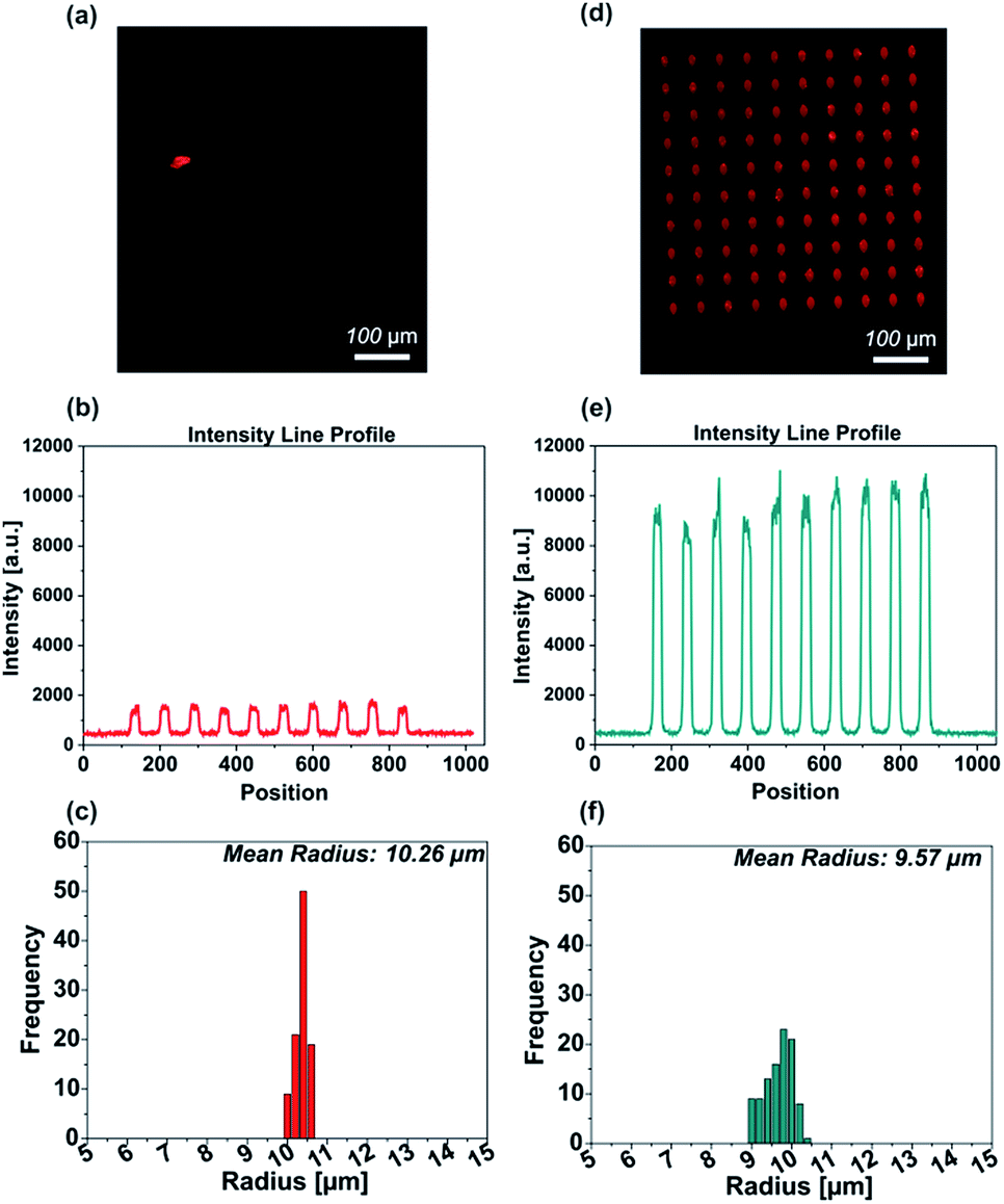 | ||
| Fig. 4 Fluorescence images of a TAMRA-azide microarray on NCD surfaces modified with propargylamine (a) and dibenzocyclooctyne-amine (d). Intensity profiles of line through one row of spots (b and e). Histograms of the spot radius of the images (a and d) are given in (c and f). | ||
To demonstrate a catalyst-free click chemistry reaction on the NCD film, a dibenzocyclooctyne-modified NCD substrate was employed for the printing of the ink solution containing TAMRA-azide but neither CuSO4 nor reducing agent. The obtained fluorescence image (Fig. 4d) shows a homogeneous binding of the ink over the whole pattern area after the washing procedure. In contrast to the propargyl-modified NCD surface, a markedly higher fluorescence signal was observed for patterns written on the DBCO-modified NCD surfaces, i.e. where the SPAAC click reaction took place. Furthermore, the intensity profile across one line of spots exhibits a uniform distribution and the average spot radius was 9.5 μm (Fig. 4e and f). In both cases, a narrow distribution of the spot sizes is observed. The significantly increased fluorescence observed on the DBCO-modified NCD surfaces after μCS with the TAMRA-azide solution with respect to the propargyl-functional NCD surface indicates that the SPAAC reaction proceeds more rapidly and effectively in comparison with the established CuAAC. Thus, SPAAC could be used to achieve the effective functionalization of the surface after 1 h of reaction following the printing procedure.
3.4 Multicomponent arrays
Multicomponent patterns are a valuable tool as they demonstrate the potential use of the protocol for creating microarrays, important for various types of sensing devices.9 In previous works, we have applied several scanning-probe-based patterning techniques in combination with CuAAC for the fabrication of such arrays.24Due to the interest in eliminating the need for the Cu-catalyst, in the current work we fabricated multicomponent arrays employing DBCO-modified NCD substrates. This approach enabled us to assess the effectiveness of the SPAAC reaction for such purpose. For the formation of multicomponent patterns the SPT was first loaded with TAMRA-azide ink and the first sub-pattern of 50 spots was written. Subsequently, the same procedure was applied for the inks Alexa Fluor 488-azide and Cy5-azide, respectively. Fig. 5a shows the results of fluorescence measurement after the binding and washing steps. The image evidences the formation of well-resolved sub-patterns from the three different fluorescent dyes. Fig. 5b shows a typical fluorescence intensity profile measured along a horizontal line in the multi-component array. It can be seen that while TAMRA-azide shows a stronger signal than Alexa Fluor 455-azide or Cy5-azide, the intensities corresponding to each sub-pattern are highly reproducible. Thus, the possibility to encode the NCD surface with multiple inks containing azide-functional molecules in a rapid catalyst-free approach is demonstrated. This is of high relevance for the fabrication of biochips, which can exploit the properties of the NCD film.
 | ||
| Fig. 5 Fluorescence image of a three spot array (TAMRA azide, Alexa Fluor 488 azide, Cy5-azide) on DBCO-modified NCD surface (a). Intensity profile of line through one row of spots (b). | ||
Arguably, a possible limitation of printing techniques based on scanning probe tools is their low throughput. Importantly, in the case of DPN and related methods, this problem can be easily overcome by parallelization of the process.70,71 This is achieved by fixing several scanning probe tools in parallel while the sample stage is scanned. Thus, the same pattern can be printed many times simultaneously significantly increasing the throughput, which is of relevance for translation of such methods to practical applications.
4 Conclusions
A new route for the covalent surface functionalization of nanocrystalline diamond films via catalyst-free click chemistry utilizing spotting with microchannel cantilevers (μCS) was introduced. This could be achieved by following a very simple surface modification protocol applied to the NCD film. Moreover, we demonstrated the ability to perform multicomponent patterns using inks containing three different azide-functional molecules and applying them onto the dibenzocyclooctyne-modified NCD surface. Results presented herein indicate that formation of a multicomponent micropattern on the modified NCD surface by μCS represents a promising strategy for the fabrication of high-density arrays that will be useful in fields such as gas sensors, biosensors, as well as optical devices.Acknowledgements
M. D. gratefully acknowledges the support from the Czech Science Foundation via grant 14-06054P. This work was partly carried out with the support of Karlsruhe Nano Micro Facility (KNMF, http://www.kmf.kit.edu), a Helmholtz Research Infrastructure at Karlsruhe Institute of Technology (KIT, http://www.kit.edu), and the Center for Polymer Technology (CPT) at DWI – Leibniz Institute for Interactive Materials.Notes and references
- M. Davydova, A. Kromka, P. Exnar, M. Stuchlik, K. Hruska, M. Vanecek and M. Kalbac, Phys. Status Solidi A, 2009, 206, 2070–2073 CrossRef CAS.
- A. Denisenko, A. Romanyuk, C. Pietzka, J. Scharpf and E. Kohn, Diamond Relat. Mater., 2010, 19, 423–427 CrossRef CAS.
- K. Haenen, K. Meykens, M. Nesladek, G. Knuyt, L. M. Stals, T. Teraji, S. Koizumi and E. Gheeraert, Diamond Relat. Mater., 2001, 10, 439–443 CrossRef CAS.
- A. Kromka, O. Babchenko, T. Izak, K. Hruska and B. Rezek, Vacuum, 2012, 86, 776–779 CrossRef CAS.
- K. Tsugawa, M. Ishihara, J. Kim, Y. Koga and M. Hasegawa, Phys. Rev. B: Condens. Matter Mater. Phys., 2010, 82, 125460 CrossRef.
- P. Rath, S. Ummethala, C. Nebel and W. H. P. Pernice, Phys. Status Solidi A, 2015, 212, 2385–2399 CrossRef CAS.
- M. Davydova, P. Kulha, A. Laposa, K. Hruska, P. Demo and A. Kromka, Beilstein J. Nanotechnol., 2014, 5, 2339–2345 CrossRef CAS PubMed.
- P. Rath, M. Hirtz, G. Lewes-Malandrakis, D. Brink, C. Nebel and W. H. P. Pernice, Adv. Opt. Mater., 2015, 3, 328–335 CrossRef CAS.
- C. Hébert, S. Ruffinatto and P. Bergonzo, in Carbon for Sensing Devices, ed. D. Demarchi and A. Tagliaferro, Springer International Publishing, Cham, 2015, pp. 227–267 Search PubMed.
- M. Davydova, M. Stuchlik, B. Rezek, K. Larsson and A. Kromka, Sens. Actuators, B, 2013, 188, 675–680 CrossRef CAS.
- P. Villalba, M. K. Ram, H. Gomez, A. Kumar, V. Bhethanabotla and A. Kumar, Mater. Sci. Eng., C, 2011, 31, 1115–1120 CrossRef CAS.
- A. Kromka, M. Davydova, B. Rezek, M. Vanecek, M. Stuchlik, P. Exnar and M. Kalbac, Diamond Relat. Mater., 2010, 19, 196–200 CrossRef CAS.
- V. Vermeeren, S. Wenmackers, P. Wagner and L. Michiels, Sensors, 2009, 9, 5600–5636 CrossRef CAS PubMed.
- C. Rodriguez-Emmenegger, C. M. Preuss, B. Yameen, O. Pop-Georgievski, M. Bachmann, J. O. Mueller, M. Bruns, A. S. Goldmann, M. Bastmeyer and C. Barner-Kowollik, Adv. Mater., 2013, 25, 6123–6127 CrossRef CAS PubMed.
- J. M. Collins, R. T. Lam, Z. Yang, B. Semsarieh, A. B. Smetana and S. Nettikadan, Lab Chip, 2012, 12, 2643–2648 RSC.
- C. C. Wu, D. N. Reinhoudt, C. Otto, V. Subramaniam and A. H. Velders, Small, 2011, 7, 989–1002 CrossRef CAS PubMed.
- L. S. Wong, F. Khan and J. Micklefield, Chem. Rev., 2009, 109, 4025–4053 CrossRef CAS PubMed.
- D. S. Engstrom, B. Porter, M. Pacios and H. Bhaskaran, J. Mater. Res., 2014, 29, 1792–1816 CrossRef CAS.
- Y. Liu and J. Yu, Microchim. Acta, 2015, 183, 1–19 CrossRef.
- A. B. Braunschweig, F. Huo and C. A. Mirkin, Nat. Chem., 2009, 1, 353–358 CrossRef CAS PubMed.
- J. Xu, M. Lynch, J. L. Huff, C. Mosher, S. Vengasandra, G. Ding and E. Henderson, Biomed. Microdevices, 2004, 6, 117–123 CrossRef CAS PubMed.
- M. Ghatkesar, H. Garza, F. Heuck and U. Staufer, Micromachines, 2014, 5, 954–1001 CrossRef.
- L. Huang, A. B. Braunschweig, W. Shim, L. Qin, J. K. Lim, S. J. Hurst, F. Huo, C. Xue, J. W. Jang and C. A. Mirkin, Small, 2010, 6, 1077–1081 CrossRef CAS PubMed.
- M. Hirtz, A. M. Greiner, T. Landmann, M. Bastmeyer and H. Fuchs, Adv. Mater. Interfaces, 2014, 1, 1300129 CrossRef.
- M. Hirtz, W. Feng, H. Fuchs and P. A. Levkin, Adv. Mater. Interfaces, 2016, 3 DOI:10.1002/admi.201500469.
- H. C. Kolb, M. G. Finn and K. B. Sharpless, Angew. Chem., Int. Ed., 2001, 40, 2004–2021 CrossRef CAS.
- V. V. Rostovtsev, L. G. Green, V. V. Fokin and K. B. Sharpless, Angew. Chem., Int. Ed., 2002, 41, 2596–2599 CrossRef CAS.
- A. Barras, S. Szunerits, L. Marcon, N. Monfilliette-Dupont and R. Boukherroub, Langmuir, 2010, 26, 13168–13172 CrossRef CAS PubMed.
- T. Meinhardt, D. Lang, H. Dill and A. Krueger, Adv. Funct. Mater., 2011, 21, 494–500 CrossRef CAS.
- W. S. Yeap, M. S. Murib, W. Cuypers, X. Liu, B. van Grinsven, M. Ameloot, M. Fahlman, P. Wagner, W. Maes and K. Haenen, ChemElectroChem, 2014, 1, 1145–1154 CrossRef CAS.
- R. E. Ruther, M. L. Rigsby, J. B. Gerken, S. R. Hogendoorn, E. C. Landis, S. S. Stahl and R. J. Hamers, J. Am. Chem. Soc., 2011, 133, 5692–5694 CrossRef CAS PubMed.
- M. R. Das, M. Wang, S. Szunerits, L. Gengembre and R. Boukherroub, Chem. Commun., 2009, 2753–2755 RSC.
- M. Wang, M. R. Das, M. Li, R. Boukherroub and S. Szunerits, J. Phys. Chem. C, 2009, 113, 17082–17086 CAS.
- S. A. Yao, R. E. Ruther, L. Zhang, R. A. Franking, R. J. Hamers and J. F. Berry, J. Am. Chem. Soc., 2012, 134, 15632–15635 CrossRef CAS PubMed.
- J. C. Jewett and C. R. Bertozzi, Chem. Soc. Rev., 2010, 39, 1272–1279 RSC.
- G. S. McCarty, Nano Lett., 2004, 4, 1391–1394 CrossRef CAS.
- Q. Wang, T. R. Chan, R. Hilgraf, V. V. Fokin, K. B. Sharpless and M. G. Finn, J. Am. Chem. Soc., 2003, 125, 3192–3193 CrossRef CAS PubMed.
- J. Gierlich, G. A. Burley, P. M. Gramlich, D. M. Hammond and T. Carell, Org. Lett., 2006, 8, 3639–3642 CrossRef CAS PubMed.
- W. F. Paxton, J. M. Spruell and J. F. Stoddart, J. Am. Chem. Soc., 2009, 131, 6692–6694 CrossRef CAS PubMed.
- M. F. Debets, S. S. van Berkel, J. Dommerholt, A. T. Dirks, F. P. Rutjes and F. L. van Delft, Acc. Chem. Res., 2011, 44, 805–815 CrossRef CAS PubMed.
- N. J. Agard, J. A. Prescher and C. R. Bertozzi, J. Am. Chem. Soc., 2004, 126, 15046–15047 CrossRef CAS PubMed.
- R. Manova, T. A. van Beek and H. Zuilhof, Angew. Chem., Int. Ed., 2011, 50, 5428–5430 CrossRef CAS PubMed.
- C. F. Wang, E. M. Makila, M. H. Kaasalainen, D. Liu, M. P. Sarparanta, A. J. Airaksinen, J. J. Salonen, J. T. Hirvonen and H. A. Santos, Biomaterials, 2014, 35, 1257–1266 CrossRef CAS PubMed.
- A. Kuzmin, A. Poloukhtine, M. A. Wolfert and V. V. Popik, Bioconjugate Chem., 2010, 21, 2076–2085 CrossRef CAS PubMed.
- S. V. Orski, A. A. Poloukhtine, S. Arumugam, L. Mao, V. V. Popik and J. Locklin, J. Am. Chem. Soc., 2010, 132, 11024–11026 CrossRef CAS PubMed.
- M. A. Wijdeven, C. Nicosia, A. Borrmann, J. Huskens and F. L. van Delft, RSC Adv., 2014, 4, 10549 RSC.
- S. V. Orski, G. R. Sheppard, S. Arumugam, R. M. Arnold, V. V. Popik and J. Locklin, Langmuir, 2012, 28, 14693–14702 CrossRef CAS PubMed.
- Y. Li, M. Giesbers, M. Gerth and H. Zuilhof, Langmuir, 2012, 28, 12509–12517 CrossRef CAS PubMed.
- J. Escorihuela, A. T. M. Marcelis and H. Zuilhof, Adv. Mater. Interfaces, 2015, 2, 1–42 Search PubMed.
- M. Abramoff, P. Magalhaes and S. Ram, Biophotonics International, 2004, 36–42 Search PubMed.
- J. H. Scofield, J. Electron Spectrosc. Relat. Phenom., 1976, 8, 129–137 CrossRef CAS.
- S. Tanuma, C. J. Powell and D. R. Penn, Surf. Interface Anal., 2005, 37, 1–14 CrossRef CAS.
- C. E. Nebel, B. Rezek, D. Shin, H. Uetsuka and N. Yang, in Physics and Applications of CVD Diamond, ed. S. Koizumi, C. Nebel and M. Nesladek, Wiley-VCH Verlag GmbH & Co. KGaA, Weinheim, Germany, 2008, ch. 6, pp. 129–176 Search PubMed.
- G. Cicala, D. Monéger, D. Cornacchia, P. Pesce, V. Magaletti, G. Perna, V. Capozzi and M. Tamborra, Surf. Coat. Technol., 2012, 211, 152–157 CrossRef CAS.
- J. A. Mucha, D. L. Flamm and D. E. Ibbotson, J. Appl. Phys., 1989, 65, 3448 CrossRef CAS.
- M. Frenklach and H. Wang, Phys. Rev. B: Condens. Matter Mater. Phys., 1991, 43, 1520–1545 CrossRef CAS.
- Š. Potocký, O. Babchenko, K. Hruška and A. Kromka, Phys. Status Solidi B, 2012, 249, 2612–2615 CrossRef.
- C. Popov, W. Kulisch, S. Bliznakov, G. Ceccone, D. Gilliland, L. Sirghi and F. Rossi, Diamond Relat. Mater., 2008, 17, 1229–1234 CrossRef CAS.
- J. Zhu, S. Wei, I. Y. Lee, S. Park, J. Willis, N. Haldolaarachchige, D. P. Young, Z. Luo and Z. Guo, RSC Adv., 2012, 2, 1136–1143 RSC.
- J. Zhu, S. Wei, J. Ryu, M. Budhathoki, G. Liang and Z. Guo, J. Mater. Chem., 2010, 20, 4937 RSC.
- J. Zhu, S. Wei, A. Yadav and Z. Guo, Polymer, 2010, 51, 2643–2651 CrossRef CAS.
- R. A. Shircliff, P. Stradins, H. Moutinho, J. Fennell, M. L. Ghirardi, S. W. Cowley, H. M. Branz and I. T. Martin, Langmuir, 2013, 29, 4057–4067 CrossRef CAS PubMed.
- M. R. Alexander, R. D. Short, F. R. Jones, W. Michaeli and C. J. Blomfield, Appl. Surf. Sci., 1999, 137, 179–183 CrossRef CAS.
- P. M. Dietrich, S. Glamsch, C. Ehlert, A. Lippitz, N. Kulak and W. E. S. Unger, Appl. Surf. Sci., 2016, 363, 406–411 CrossRef CAS.
- S. Oberhansl, M. Hirtz, A. Lagunas, R. Eritja, E. Martinez, H. Fuchs and J. Samitier, Small, 2012, 8, 541–545 CrossRef CAS PubMed.
- B. Gold, G. B. Dudley and I. V. Alabugin, J. Am. Chem. Soc., 2013, 135, 1558–1569 CrossRef CAS PubMed.
- P. A. Ledin, N. Kolishetti and G. J. Boons, Macromolecules, 2013, 46, 7759–7768 CrossRef CAS PubMed.
- N. Zydziak, C. M. Preuss, V. Winkler, M. Bruns, C. Hubner and C. Barner-Kowollik, Macromol. Rapid Commun., 2013, 34, 672–680 CrossRef CAS PubMed.
- M. Hirtz, M. Lyon, W. Feng, A. E. Holmes, H. Fuchs and P. A. Levkin, Beilstein J. Nanotechnol., 2013, 4, 377–384 CrossRef PubMed.
- K. Salaita, Y. Wang, J. Fragala, R. A. Vega, C. Liu and C. A. Mirkin, Angew. Chem., Int. Ed., 2006, 45, 7220–7223 CrossRef CAS PubMed.
- J. Xu, M. Lynch, S. Nettikadan, C. Mosher, S. Vegasandra and E. Henderson, Sens. Actuators, B, 2006, 113, 1034–1041 CrossRef CAS.
Footnote |
| † Electronic supplementary information (ESI) available. See DOI: 10.1039/c6ra12194b |
| This journal is © The Royal Society of Chemistry 2016 |