Wei Liab,
Yansong Wanga,
Mengmeng Wanga,
Wenjiang Lia,
Junjun Tanc,
Chen You*a and
Minfang Chen*ab
aSchool of Materials Science and Engineering, Tianjin University of Technology, Tianjin, 300384, China. E-mail: mfchentj@126.com; Tel: +86 022 60215845
bTianjin Key Lab for Photoelectric Materials & Devices, Tianjin, 300384, China
cSchool of Chemical and Materials and Engineering, Hubei University of Technology, Hubei 435003, China
First published on 22nd June 2016
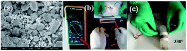
Highly conductive flexible paper-based patterns were drawn directly using a brush pen dipped in ink consisting of copper–silver core–shell with individual silver (CucoreAgshell&Ag) particles. Using a cost-effective and green method, the formation of these CucoreAgshell&Ag particles is first driven by a transmetalation reaction on the surface of copper nanoparticles between copper atoms and silver ions, and then excessive Ag ions were further reduced by the glucose to form individual Ag nanoparticles. Characterization of these particles by XRD, SEM and TGA confirm the CucoreAgshell&Ag structure and their stability towards oxidation. The conductivity of the bending pattern was experimentally tested with different bending angles, bending cycles and bending storage times. It was found that the silver shell with external excessive Ag NPs not only improves the packing density, but also enhancing the particle purity results in the high conductivity of the bending pattern. Sintered at a low temperature of 160 °C and after 3000 bending cycles and storage for 300 days, the linear resistivity of the pattern increased from ∼5 μΩ cm to ∼20 μΩ cm, 4 times higher than before the pattern was bent, which is acceptable for conductive patterns in practical applications. Thus, this approach represents a promising method for the formation of microelectrodes or electronic devices with good flexibility and conductivity.
Conductive ink materials including carbon,5 conductive polymer,6 graphene,7 or metal–organic complex8 inks have been used in the formation of conductive patterns, but these materials typically exhibit low electrical conductivity and low resolution, poor chemical and thermal stability, and there are few reports on the preparation of these materials through a green method. Although noble metal NPs, such as gold and silver NPs, possess high conductivity and can be used as alternative materials,9–11 the high cost of these materials has limited their commercial applications. The use of the much cheaper copper with good conductivity is highly anticipated, but it is easily oxidized into either Cu2O or CuO under ambient conditions leading to an increase in the sintering temperature, greatly reducing the electrical conductivity of the pattern.12 Some anti-oxidation materials, such as silver and carbon, have been used as the shell of a Cu core.13,14 However, the thin-shell layer was easily broken when sintered at a high temperature, reducing the pattern’s conductivity.14 In addition, with the increase of the packing density of micrometer-sized metal patterns upon adding different size particles, the pattern’s electrical conductivity can be improved.15–17 So mixed metal-based inks,12,18 such as Ag and Cu, have been developed recently. However, this material, formed by the simple addition of particles, was easily oxidized after storage for a long time. Obviously, there is still a need to develop a new-type of conductive ink to solve the above mentioned problems. For the reported conductive and flexible patterns,19 the mechanical properties is an important factor for its practical application. However, there are very few reports on the patterns’ conductivity and microstructure when the patterns were bent or kept in bent shape for a long time.20,21
Here, we report a simple and green method to synthesise air-stable CucoreAgshell&Ag particles via mixed polyvinylpyrrolidone (PVP) and cetyltrimethylammonium bromide (CTAB) as capping agents, and made a corresponding conductive ink, which can be used to directly write on photo paper. Flexible paper-based patterns, sintered at a low temperature of 160 °C, were obtained. The conductivity, mechanical flexibility and microstructure of the patterns were investigated with different bending angles, number of bending cycles and bending storage time. This CucoreAgshell&Ag particle structure has an advantage in enhancing the flexibility of the pattern with minimal degradation of its electrical properties. Furthermore, using this simple method, flexible and conductive paper-based microelectrodes can be fabricated easily.
To build a surface tension gradient between the solvents to acquire high quality CucoreAgshell&Ag ink, the obtained CucoreAgshell&Ag particles were redissolved into a mixture of water, ethanol, glycerol and ethylene glycol (their corresponding surface tensions being 72.8, 22.4, 63.3, 48.5 mN m−1, respectively) with corresponding vol% values of about 23.0:
8.0
:
30.5
:
38.5. The CucoreAgshell&Ag NPs were dispersed by ultrasonic treatment to obtain 35 wt% CucoreAgshell&Ag ink and used for drawing flexible printed patterns.
Cu2+ + H2PO2− + H2O → Cu↓ + H2PO3− + 2H+ | (I) |
2[Ag(NH3)2]2OH + C6H12O6 → 2Ag↓ + 3NH3↑ + H2O + CH2OH(CHOH4)COONH4 | (II) |
Cu + 2Ag+ → Cu2+ + 2Ag↓ | (III) |
XRD patterns of the synthesized samples are shown in Fig. 2. As seen from line a in Fig. 2, without the silver nitrate solution being added to the solution, the diffraction peaks of the pure Cu particle sample presents three main characteristic peaks at 2θ = 43.3°, 50.4° and 74.08°, corresponding to the Miller indices (111), (200) and (220) of metallic Cu with a face-centered cubic (fcc) structure. While, as can be seen going from line a to line b, upon adding silver nitrate to the solution with the Cu NPs, we can see that the obtained particles not only show the crystalline copper characteristic peaks, but also show four characteristic peaks at 2θ = 38.2°, 44.2°, 64.4° and 77.4°, corresponding to the diffraction peaks of (111), (200), (220) and (311) of face-centered cubic (fcc) Ag, indicating the presence of both copper and silver with fcc crystal structures. Moreover, increasing the concentration of silver nitrate resulted in enhancing the diffraction intensity of the Ag phase (line c), and meanwhile, the crystalline copper characteristic peaks disappeared, indicating that the CucoreAgshell&Ag particles were observed.
![]() | ||
Fig. 2 X-ray diffraction patterns for the obtained particles with different concentrations of AgNO3 from (a) 0 g L−1 to (b) 51 g L−1 and (c) 102 g L−1 in 10 mL. |
Fig. 3 shows SEM images of obtained particles and their particle size distributions. Many small particles among large particles were shown in Fig. 3a and d; the larger particle size is 1.1 ± 0.1 μm and the smaller particle size is 0.06 ± 0.04 μm. The number of small particles was not enough to be coated completely on the surface of the large particles, resulting in part CucoreAgshell particles obtained. This result was consistent with the XRD result from line b in Fig. 1. Upon increasing the silver nitrate concentration, more and more small particles with a size of 0.06 ± 0.04 μm appeared among the larger particles and the large particles became more and more large with a size of 1.7 ± 0.5 μm (Fig. 3b and e). Compared with the XRD result from line c in Fig. 1, this result indicates that CucoreAgshell&Ag particles were obtained. The core–shell structure of the CucoreAgshell&Ag particles was seen and the light silver shell was coated on the surface of the dark copper core, surrounded with small particles (ESI Fig. S1†). Fig. 2c shows the obtained spherical silver particles with a large distribution and a size of 0.06 ± 0.02 μm (Fig. 3f), which have a similar distribution tendency to the small particle distribution tendency in the inset images in Fig. 3d and e, indicating that the small particles were silver and the larger particles were copper.
Fig. 4 shows thermogravimetric curves of the CucoreAgshell&Ag particles obtained at temperatures ranging from room temperature to 700 °C in air. According to a previous report,22 the weight gain of the obtained particles occurs in four steps: (I) the first step from room temperature to 220 °C is a fast weight loss, attributed to the loss of residual alcohol and physisorbed water in the material and the weight loss was about 3%. (II) As the temperature increased between 220–400 °C, there was a low rate decomposition and oxidation stage as the organic capping layer gradually decomposed and the sample gained weight as the Ag NPs started to oxidize. In fact, the thermal decomposition of pure CTAB molecules was mainly performed at this temperature (Td = 200–300 °C). Because the gain weight is higher than the loss weight, the gain weight was partially offset, which was only about 0.9%. (III) The third step was a rapid oxidation stage at 400–550 °C, due to the weight loss from the accelerated decomposition of the residual organic molecules (mainly PVP, Td = 400–500 °C) and weight gain from the oxidation of silver or copper particles. The weight gain is much higher than the weight loss, so the weight gain increased greatly by about 2.3%. (IV) As the temperature increased ranging from 550 to 700 °C, weight gain or loss is not obvious, indicating that the oxidation process of silver or copper was completed. In theory, with all silver particles oxidized the weight gain was about 6.1% (molar ratio of Cu:
Ag = 1
:
3), which was higher than the total virtual weight gain 3.1% in stages II and III; considering the partial offset of the weight loss of the organic capping molecules (<0.9%), more Ag particles were oxidized and the Ag shell was not completely oxidized, indicating the silver shell was a dense anti-oxidation layer for copper particles. These results suggested that the excess silver particles and silver shell, forming a dense layer, made the obtained pattern possess a high electrical conductivity even when the temperature was raised to 400 °C. Based on this result, more substrates needing a higher temperature can be used in more fields of application.
![]() | ||
Fig. 5 Applications of paper-based CucoreAgshell&Ag conductive patterns drawn using a brush pen sintered at 160 °C for 2 h. |
The lowest resistivity of the pattern at a low temperature 160 °C is related to the state of the coated Cu particles. As illustrated in Fig. 6, in the form of CucoreAgshell, the silver shell transforms during heating into small particles, which are attached to the copper core surface, and above 250 °C, the Cu particles are no longer coated by a silver shell.14 However, in the form of CucoreAgshell&Ag, existing excess Ag particles resist the shell transformation into small particles, the Cu NPs are still coated by a silver shell at a high temperature, and this structure not only improved the high conductivity and increased the flexibility of the pattern after sintering at 250 °C for 2 h and 3000 bending cycles (ESI Fig. S3†). This explanation is consistent with the thermogravimetric curves of the CucoreAgshell&Ag particles.
![]() | ||
Fig. 6 Schematic illustration of the growing silver crystallites forming shells as CucoreAgshell and CucoreAgshell&Ag, respectively. |
To further test the flexibility of the patterns, the bending pattern was kept at 330° and the resistance was measured as a function of storage time. The resistivity curve was shown in Fig. 8. When the storage time was increased from 0 to 100 days, owing to the blocked conduction path between the particles, the patterns’ resistivity gradually increased from ∼16.2 to 37.5 μΩ cm. While with the increase of the storage time to 300 days, the resistivity changed insignificantly, ∼38.5 μΩ cm, indicating that the blocked conduction path between the particles was stable, and this relatively low resistivity is also acceptable for practical application.
![]() | ||
Fig. 8 The resistivity of the CucoreAgshell&Ag patterns with bending kept at 330° as a function of storage time; the inset shows the corresponding resistance of the bending pattern. |
Surface microstructures of the patterns sintered at 160 °C for 2 h before and after bending were observed by SEM (Fig. 9). It can be clearly seen that before bending, the surface of the pattern was composed of many excess particles (Fig. 9a), and the excessive smaller Ag NPs were able to fill the interstices between the larger CucoreAgshell particles, which was similar to the earlier reported single CucoreAgshell particles sintered at 250 °C,14 resulting in an increase in densification. These results indicate that the existence of excessive smaller Ag NPs leads to the pattern with a relatively low resistivity 5 μΩ cm (Fig. 5) at a lower temperature of 160 °C. After the bending pattern was kept at 330° for 300 days (Fig. 9b and e), the void spaces on the surface of the pattern became more obvious and from the cross-sectional area of the pattern (Fig. 9c and f), more small grooves and cracks were obvious, leading to the resistivity of the pattern increasing to 38.5 μΩ cm, which was about two orders of magnitude lower than that of the single Cu and Ag particles (the resistivity was ∼1.0 × 10³ μΩ cm and 1.9 × 10³ μΩ cm, respectively, ESI Fig. S2†). These results demonstrate that the conductive property of the pattern was affected by its microstructure, which is related to its particle densification. In theory, with the increase of the patterns’ bending angle, the distance between particles would gradually increase, especially the upwards surface of the pattern, leading to a decrease of the conductivity of the pattern. However, the CucoreAgshell&Ag patterned microelectrodes can withstand repeated bending and stretching to large levels of strain with partial degradation of their electrical properties. Thus, a quality CucoreAgshell&Ag pattern with low resistivity and high flexibility was obtained.
Fig. 10 shows the electrical resistivity of the CucoreAgshell&Ag pattern as a function of bending cycles with different measured conditions. The bending angle was kept at 330° (Fig. 7c). Increasing the number of bending cycles, measuring the sample whilst curved, the resistivity of the pattern greatly increases over less than 1000 cycles, and over 3000 cycles, the resistivity was 110 μΩ cm, which was higher than before bending. However, under linear measured conditions, the resistivity changed insignificantly from ∼20 μΩ cm, 3 times before bending over 3000 cycles, which indicates that the number of microcracks or void space was decreased and a conduction path was formed. We believe that the microcracks or void space was increased with the pattern being gradually bent and decreased with the existence of excessive small Ag NPs in the CucoreAgshell&Ag structures, resulting in the pattern possessing an acceptably lower resistivity with good flexibility. Thus, in the future, the conductivity of flexible patterns can be improved using stretchable conductive materials to avoid microcracks or void spaces.
![]() | ||
Fig. 10 Electrical resistivity of the patterns as a function of bending cycles and measured before and after bending (named curve resistivity and linear resistivity), respectively. |
Surface microstructures of the patterns sintered at 160 °C for 2 h after 3000 bending cycles were observed by SEM (Fig. 11). It can be clearly seen that the void space on the surface of the pattern became more and more obvious (Fig. 11a), and from the cross-sectional area of the pattern (Fig. 9b), more small grooves and cracks were observed, leading to the resistivity of the pattern increasing to 110 μΩ cm. This is also confirmed by the ordinary small bulb operation of the bending pattern, displaying a weak light in the inset of Fig. 11a. For the single Ag or Cu patterns, a lamp can not be turned on under the same conditions, indicating that larger cracks were formed. These results demonstrate that the conductive property of the pattern was affected by its microstructure, related to its particle densification, and adding more small Ag NPs between the CucoreAgshell particles increases the densification, resulting in an increase in the patterns’ conductivity. Thus, the ink with CucoreAgshell&Ag particles is appropriate to be used as conductive materials, and the photo paper guarantees the flexibility and foldability of the substrate.
Footnote |
† Electronic supplementary information (ESI) available. See DOI: 10.1039/c6ra11965d |
This journal is © The Royal Society of Chemistry 2016 |