
Highly proton conducting MoS2/graphene oxide nanocomposite based chemoresistive humidity sensor†
Debasree Burmana,
Ruma Ghosha,
Sumita Santrab and
Prasanta K. Guha*a
aDepartment of Electronics & Electrical Communication Engineering, Indian Institute of Technology, Kharagpur, W. B. 721302, India. E-mail: pkguha@ece.iitkgp.ernet.in; Tel: +91 3222 283538
bDepartment of Physics, Indian Institute of Technology, Kharagpur, W. B. 721 302, India
First published on 26th May 2016
Abstract
This paper reports the development of MoS2/GO nanocomposite based sensing layers for resistive humidity sensors. The MoS2 nanoflakes were synthesized through liquid exfoliation and GO was synthesized using modified Hummers method. The nanocomposite was drop-cast on a Si/SiO2 substrate containing aluminium electrodes to fabricate the sensor device. The best performance was shown by the 1![[thin space (1/6-em)]](https://www.rsc.org/images/entities/char_2009.gif) :4 (MoS2/GO) composite. Various characterization techniques like Scanning Electron Microscopy (SEM), Transmission Electron Microscopy (TEM), X-Ray Diffraction (XRD), X-ray Photoelectron Spectroscopy (XPS), and Fourier Transform Infrared Spectroscopy (FTIR) were used to verify the composite formation. The sensing response was found to lie between 55 times at 35% RH and 1600 times at 85% RH. Such a high response is believed to be because of proton conductivity in the water layer for both MoS2 and GO. The sensor performance was found to be repeatable even after three months of the first measurement with quick response and recovery. Thus the authors believe that the excellent sensitivity coupled with low cost synthesis and resistive sensing will make their work useful to develop new generation humidity sensors.
:4 (MoS2/GO) composite. Various characterization techniques like Scanning Electron Microscopy (SEM), Transmission Electron Microscopy (TEM), X-Ray Diffraction (XRD), X-ray Photoelectron Spectroscopy (XPS), and Fourier Transform Infrared Spectroscopy (FTIR) were used to verify the composite formation. The sensing response was found to lie between 55 times at 35% RH and 1600 times at 85% RH. Such a high response is believed to be because of proton conductivity in the water layer for both MoS2 and GO. The sensor performance was found to be repeatable even after three months of the first measurement with quick response and recovery. Thus the authors believe that the excellent sensitivity coupled with low cost synthesis and resistive sensing will make their work useful to develop new generation humidity sensors.
Introduction
The necessity of continuous monitoring of humidity in various fields starting from industrial processing, environmental control, manufacturing of highly sophisticated integrated circuits in the semiconductor industry, the automobile industry, and agriculture1 has led to an increased demand for highly sensitive, low cost, wide range, fast humidity sensors. In a recent survey it has been estimated that the humidity sensor market will reach ∼$ 2.3 billion by 2020.2Based on transduction techniques, humidity sensors can be classified as resistive,3 capacitive,4 optical fibre based,5 field effect transistor (FET),6 Surface Acoustic Wave (SAW),7 Quartz Crystal Microbalance (QCM)8 etc. Among these, capacitive humidity sensors are most widely used. In fact, most of the commercially available humidity sensors are based on a capacitive technique where the dielectric constant of a polymer layer changes in the presence of humidity. However, capacitive sensors have their own limitations like hysteresis, stability at high temperature and humidity levels as well as durability against some organic vapours.9 Also, such sensors are expensive. On the contrary, resistive humidity sensors have simpler structure and they are easier to integrate with Complementary Metal Oxide Semiconductor (CMOS) technology than capacitive sensors. Hence a lot of research is currently being focussed on development of resistive humidity sensors which is believed to reduce the cost of per unit sensor and also their long time stability will be more.
The most commercially used sensing materials for humidity detection are porous ceramics and polymer films10 (e.g. Greystone,11 Johnson Controls12). The polymer films are unable to operate at high humidity levels, show hysteresis, slow response time and long term drift. Although humidity sensors using metal oxides as sensing layer are also commercially available (e.g. Honeywell humidity sensors13), the disadvantage is such sensor requires periodic heat cleaning to recover its humidity sensing properties. The sensors also exhibit a progressive shift of resistance due to gradual formation of chemisorbed hydroxyl ions on the surface of the sensing layer.14 Again, several groups are involved to develop high performance humidity sensing nanomaterials like silicon nanostructures,15 ceramic nanomaterials,1 semiconductor nanoparticles16 and metal oxide nanowires.3,14,17–21 There have also been recent reports of graphene and its derivatives (e.g. reduced graphene oxide (RGO) and graphene oxide (GO)) as humidity sensing layers.3,21–23 GO can act as a good humidity sensor because of the presence of large functional groups, inherent defect sites and formation of large proton conducting paths in presence of humidity. However pure graphene lacks in defect sites and thus its sensitivity towards humidity is low.24 Recently, two dimensional transition metal dichalcogenides like molybdenum disulphide (MoS2) have received increasing attention for ultrasensitive sensor applications.25,26 MoS2 is a layered metal dichalcogenide which consists of hexagonal rings of S–Mo–S atoms held together by weak van der Waals force of interaction. The presence of layered structure and inherent defects make it an ideal candidate as the sensing material for humidity sensors. However, there have been very few reports on MoS2 based humidity sensors as per the knowledge of the authors.6,27–29 The MoS2 based FET in Rao et al.'s paper did not show significant response till a relative humidity (RH) level of 60%.6 Zhang et al. showed a response value of only 3 times using their MoS2 based thin film sensor device.27 Using their capacitive sensor, Zhu et al. observed a sensitivity of around 32.19 nF/%RH at 89.5% RH.28
Thus humidity sensors made of pure MoS2 suffer from low sensitivity at room temperature as has been reported already. Hence to increase the sensitivity of MoS2 based humidity sensor, it can be functionalized with other nanomaterials or metal nanoparticles. However, doping with noble metals would increase the per capita cost of the sensor.
In our paper, we are reporting for the first time the development of an excellent humidity sensing layer based on MoS2/GO nano-composite. The MoS2 nanoflakes were obtained using liquid exfoliation technique and GO was prepared by the well-known modified Hummers method. The proportion of GO was varied to get optimized performance. The composites were extensively characterized using different material characterization techniques. The response of the sensors was carried out at six different humidity levels between 35% and 85% RH. The optimized sample showed response as high as 1600 times at 85% RH. The optimized sample was further tested for stability, repeatability and hysteresis. The detailed results and the probable sensing mechanism have been explained in this manuscript.
Experimental section
Chemicals required
MoS2 powder (Sigma Aldrich, <2 μm, 99%) and absolute ethanol were required for the exfoliation of MoS2 nanoflakes. Graphite powder, NaNO3, H2SO4 (98%), H2O2 (30%), KMnO4 were used to exfoliate graphene oxide from bulk graphite powder. All the chemical reagents were of analytical grade.MoS2 synthesis
In our laboratory, MoS2 nanoflakes were exfoliated from bulk MoS2 powder using a sonication assisted exfoliation technique. 75 mg of MoS2 powder (<2 μm, 99%, Alfa Aesar) was added to 45% ethanol water. The solution was then sonicated for 8 hours in a Microclean 102 ultrasonic bath. In order to study the effect of particle size on the sensing response, three other samples with different sonication times of 2 hours, 4 hours and 12 hours were also prepared. After sonication, the dispersion was centrifuged at 4500 rpm to remove the residue/precipitate and the yellowish green supernatant containing the nanoflakes was collected.Graphene oxide synthesis
GO was synthesized using modified Hummers method.30 For our experiment, 0.5 g of graphite and 0.5 g of NaNO3 were taken in a round bottomed flask and 25 mL of 98% H2SO4 was added to it. Next, 3 g of KMnO4 was slowly added to the mixture kept in an ice bath with constant stirring. The solution was then transferred to a 40 °C water bath and constantly stirred for about 1 hour to form a thick paste. 50 mL of water was added to the solution which was again stirred for 30 minutes at 90 °C. The reaction mixture was diluted with 100 mL of water. Finally, 3 mL of H2O2 (30%) was slowly added to the dark brown solution which turned yellow. The graphene oxide cake was then filtered (vacuum filtration) and washed with 800 mL of water. The visible particles and other water soluble impurities were removed by repeated washing cycles of centrifugation and sonication.MoS2/GO composites
The MoS2 dispersion (8 hours sonicated sample) was mixed with different volumes of GO to get a number of samples with different volume ratios as MoS2/GO 1:0.33, 1:0.5, 1:1, 1:2, 1:3, 1:4, 1:6, 1:8. MoS2/GO sample 1:8 means 1 mL of MoS2 dispersion was mixed with 8 mL of GO and so on. The samples were named respectively as S0–S8 where S0 stands for the sample without any GO content and S1–S8 for the samples with progressive increase of GO proportion. Each mixture was stirred for 20 minutes to ensure proper mixing and uniform dispersion of the flakes. To perform the humidity tests, 0.4 μL of each sample was drop-casted on aluminum electrodes designed and fabricated on Si/SiO2 substrate using conventional lithography techniques. Fig. 1 shows our chemoresistive humidity sensing device.
 | ||
| Fig. 1 Schematic of our humidity sensing device. | ||
Material characterizations
In order to ensure successful exfoliation of few-layer MoS2 nanoflakes from the bulk MoS2 powder and graphene oxide from bulk graphite powder, various material characterizations were done using a number of different techniques like SEM, TEM, XRD and FT-IR. The samples were also characterized to ensure proper mixing of MoS2 and GO (i.e. presence of both the flakes). The Field Emission SEM (FESEM) was performed using SUPRA 40 field emission scanning electron microscope for the surface morphological studies. The samples were prepared by spin coating the dispersions on Si/SiO2 substrate. The High Resolution TEM (HRTEM) measurements were carried out using JEOL JEM-2100 HRTEM operated at an acceleration voltage of 200 kV. The samples for HRTEM characterization were prepared with a few drops of diluted dispersion of MoS2/GO on a standard holey carbon covered copper grid. The X-ray diffraction patterns were collected using a Panalytical X'Pert Pro Diffractometer with a conventional X-ray tube (Cu Kα radiation). The XPS characterization was carried out using PHI 5000 Versa Probe II (ULVAC-PHI Inc., Japan). FTIR spectrometry of a few samples were carried out using Fourier transform infrared spectrometer (FT-IR spectrometer), model no: NEXUS-870. The samples were prepared using KBr pellets and FT-IR was carried out in transmittance mode.Humidity sensing setup
The humidity test set up which was made in-house consisted of a stainless steel chamber to probe the samples, a test fixture AGILENT 16442A, Semiconductor Parametric Analyzer (SPA) Agilent 4155C, gas bubbler and compressed air supply. The nano-composite was initially drop-casted on patterned aluminum electrodes on Si/SiO2 substrate to fabricate the sensor device. The sensor was then placed on a vero board using a double sided tape. Copper wires were then connected to the two electrodes using silver paste. The sensor samples were probed inside the airtight stainless steel chamber which was connected to the test fixture. Fig. 2 shows the schematic of the gas sensing setup. The chamber where the sample was probed had two gas lines-one for the compressed air to enter the chamber whiles the other for humid air which reached the chamber through a gas bubbler. The relative humidity was set with the help of a commercial humidity sensor (Dolphin Automation, model no. TH-382) capable of measuring both humidity and temperature. The entire test set-up was interfaced to the SPA using the test fixture. The SPA was connected to a PC having Agilent's Desktop Easy EXPERT software, a GUI based characterization software, for efficient and repeatable device characterization in the entire characterization process. | ||
| Fig. 2 Schematic of gas sensing setup. | ||
Results and discussion
Material characterizations results
During the humidity sensing process, it was found that MoS2/GO 1:4 sample showed the maximum response. So we have tried to highlight the morphology as well as structural analysis of that sample through our characterizations.
Fig. 3 shows the FESEM images of bulk MoS2, 8 hours sonicated and exfoliated MoS2, exfoliated GO and MoS2/GO 1:4 samples respectively in Fig. 3(a), (b), (c) and (d). It is clear from the SEM images (Fig. 3(a)–(b)) that the number of stacked layers of MoS2 as well as the lateral dimension of the flakes got reduced with sonication. The MoS2 flake sizes varied from 168 nm to 1.1 μm. Fig. 3(d) shows the co-existence of both MoS2 flakes and GO sheets, thus showing a composite structure. The MoS2 layers are not uniform throughout the sample and some parts contain more number of layers than the other. This might have occurred because of restacking of nanosheets upon removal of solvent from the dispersion. The SEM images of various composites of MoS2/GO are given in the ESI (Fig. S1†). With the increase in GO proportion, it can be seen that the GO films partially or fully covering the MoS2 flakes or the latter lying on GO film. The formation of composite was further revealed from the EDAX images provided in the ESI (Fig. S2–S4†) which shows successful formation of the composite. In Tables S1 and S2,† the atomic% of Mo and S show that they exist in the atomic ratio of 1:2. Again the weight% of Mo and S reduced in MoS2/GO composite compared to that of pristine MoS2 confirming the formation of a composite with GO. Also, the presence of high proportion of carbon and oxygen confirms the presence of GO in the composite. The silicon peaks were seen as the sample was spin coated on Si substrate and the peak of gold arose from the gold coating that was required to characterize the sample. The lateral size of the GO flakes was found to be around 1.37 μm. The increase in proportion of GO was evident from the SEM images in ESI† showing a gradual increase of GO layers and decrease of MoS2 flakes.
 | ||
| Fig. 3 FESEM image of (a) bulk MoS2 powder (b) exfoliated MoS2 (c) exfoliated GO (d) MoS2/GO 1:4. | ||
In order to obtain the microstructural information of the samples, the HRTEM measurements were carried out. The TEM images and selected area diffraction (SAED) pattern of MoS2/GO 1:4 are shown in Fig. 4. The characterization reveals that the MoS2/GO composites deliver a composite structure of layered MoS2 on GO. From the TEM images (Fig. 4(a) and (b)), it was found that few layered MoS2 flakes co-exist with partially or fully overlapped layers of GO.
 | ||
| Fig. 4 (a and b) TEM images of MoS2/GO 1:4 (c) HRTEM image showing fringes of GO (d) SAED patterns of MoS2 and GO in the sample. | ||
The SAED pattern (Fig. 4(d)) confirmed the presence of various planes of MoS2 ((002) and (004)) and GO (001). It also indicated a multiple spot pattern, one of which was due to polycrystallinity of stacked GO sheets and the other one due to MoS2. The hexagonal spot pattern also confirms the crystallinity as well as hexagonal structure of the exfoliated MoS2. Moire patterns (Fig. 4(c)) were also observed that arose because of overlapping of different planes of GO. The TEM images clearly reveal a successful chemical doping of MoS2 flakes by GO.
To study the crystallographic feature of nanoflakes, the diffraction pattern was collected. The HRTEM data was verified with XRD measurement. Fig. 5 shows the comparative XRD pattern of MoS2/GO 1:4 and exfoliated MoS2 samples with the lines indexed according to ICDD-JCPDS card no. 0037-1492 for MoS2 and JCPDS card no. 75-1621 for hexagonal carbon. The interlayer spacing d002 for MoS2 has been calculated as 6.15 angstrom which matches with the reported data and it is believed that exfoliation of MoS2 occurs along the (002) plane.31 The diffraction pattern of the samples showed MoS2 peaks at 2θ = 14.4°, 29.02°, 35.99°, 39.925°, 43.045°, 49.786° and 55.01° corresponding to (002), (004), (102), (103), (006), (105) and (106) planes respectively. Sample S6 (MoS2/GO 1:4) also showed a broad peak at 2θ = 10.4° which corresponds to the (001) plane of GO. The presence of (002) plane and (004) plane of MoS2 and (001) plane of GO were also confirmed from the SAED pattern of HRTEM images.
 | ||
| Fig. 5 XRD patterns of MoS2 nanoflakes and MoS2/GO 1:4. | ||
FT-IR spectrometry of exfoliated MoS2 flakes, GO nanosheets as well as MoS2/GO 1:4 composite are shown in Fig. 6. Since MoS2 is featureless in the wavenumber range of 4000 cm−1 to 700 cm−1, the characteristic peaks in that range are due to the presence of GO. The presence of oxygen containing groups reveals that graphite has been oxidized. The peaks at 1052 cm−1, 1225 cm−1 and 1415.1 cm−1 correspond to C–O stretching vibration (alkoxy), C–O stretching vibrations (epoxide/ether) and C–OH (carboxyl) respectively. The peak at 1641 cm−1 corresponds to the stretching and bending vibration of OH groups of water molecules absorbed on graphene oxide. The surface hydroxyl groups result in the formation of hydrogen bonds between graphite and water explaining clearly the hydrophilic nature of graphene oxide. The absorbed water in GO is shown by a band between 3226 cm−1 and 3600 cm−1 contributed by OH stretch of water molecules.32 A MoS2 peak can be observed (red curve) at 473 cm−1 and it can be accounted for the bridging Mo–S bond (Mo–S vibration perpendicular to the basal plane).33
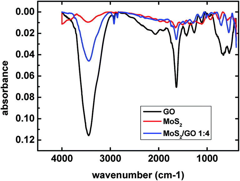 | ||
| Fig. 6 FT-IR spectrometry of MoS2, GO flakes and MoS2/GO 1:4 composite. | ||
The peak at 658 cm−1 can be assigned to S–H vibrations confirming H bonding at S edges (blue curve) and 588 cm−1 to S–S bonding strongly. The wavenumber shift strongly suggests chemical interactions between MoS2 and GO thus showing a chemical functionalization of MoS2 by GO.
The XPS characterization of the 2 hours and 8 hours sonicated MoS2 samples were also done to investigate the presence of S-vacancies in the samples. The details of the characterization have been given in the ESI (Fig. S5†).
Humidity sensing results
The chemoresistive sensor device was first exposed to compressed air for around 30 minutes to achieve a stable baseline resistance. The conductivity of the sensing layer changes in the presence of humidity.The changes in current through the sensor were measured using a SPA. The response of the sensors was calculated as
| Ihumidity/Ibaseline |
A number of humidity tests on various samples were carried out which are briefly described as follows.
The response of the MoS2 based sensor devices (i.e. the sensing layer containing only MoS2 and no GO) against different humidity levels was studied as shown in Fig. 7. All the four samples with different sonication times were exposed to three different levels of humidity viz. 45% RH, 55% RH and 65% RH, each for 10 minutes followed by compressed air purging for the next 10 minutes. The bar plot shown in Fig. 7(a) clearly shows the response of 8 hours sonicated sample was better than the remaining samples. Hence the response of the 8 hours sonicated sample was plotted separately in Fig. 7(b). The response of the sensor device was found to increase with increase in humidity levels.
 | ||
| Fig. 7 (a) Comparative response values of 2 hours, 4 hours, 8 hours and 12 hours sonicated MoS2 samples. (b) Response of 8 hours sonicated MoS2 sample for three different humidity levels. | ||
Although the 8 hours sonicated sample showed the optimised response, however, from Fig. 7(b), it is clear that pristine MoS2 nanoflakes show poor response (∼10 times for a RH level of 65%) towards humidity. The response of pristine MoS2 based humidity sensor was found to be much lower than other nanomaterial based humidity sensors.
Thus to enhance the performance of MoS2 based humidity sensor, we have tried to functionalize MoS2 nanoflakes with GO.
The GO was mixed with MoS2 in various proportions (the details have been given in the Experimental section). In order to carry out the humidity tests, each sample was tested against three different humidity levels viz. 45%, 55% and 65% RH as before. This test was repeated for all the nine samples from S0–S8. The response for one particular cycle viz. 65% RH level has been shown in Fig. 8(a). Since the optimized response was observed for MoS2/GO 1:4 composite, the sample was tested against six different humidity levels (35% RH to 85% RH) and the responses have been plotted in Fig. 8(b).
 | ||
| Fig. 8 (a) Comparative plot of response of different samples at 65% RH. (b) Response of MoS2/GO 1:4 sample for 6 different humidity levels. | ||
From the above two figures, it can be seen that the response of the samples increases with increase in humidity levels. The sensor response varied from 3 times (with 35% RH) to 1600 times (85% RH). This is much higher than previously reported results of MoS2 based humidity sensor devices (∼3 times at 60% RH,27 32.19 nF/% RH at 89.5% RH28).
The response time (ζresponse) is defined as the time taken by the sensor to reach 90% of the response after the humid air was switched on and recovery time (ζrecovery) is defined as the time taken to reach 10% of the baseline resistance after the humidity was switched off. The response time and recovery time of sample S6 (MoS2/GO 1:4) for a single cycle response of 65% RH were found to be 43 seconds and 37 seconds respectively which are better than (ζresponse = 90 s, ζrecovery = 110 s for 71.8% RH cycle28) or comparable to (ζresponse = 9 s and ζrecovery = 17 s (although response was poorer than our device27))] previously reported MoS2 based humidity sensors. The results show that we can make a fast highly sensitive humidity sensor using MoS2/GO composite.
The MoS2/GO 1:4 sample was also tested for reproducibility. It was exposed to three cycles of 65% RH, each for 10 minutes followed by 10 minutes of compressed air purging. The response of the sensor was also found to be repeatable over the three iterative cycles (Fig. 9(a)). So, it can be concluded that the MoS2/GO based sensor is reusable over a number of times.
 | ||
| Fig. 9 (a) Repeatability of MoS2/GO 1:4 sample at 65% RH. (b) Stability test of MoS2/GO 1:4 sample. | ||
In order to ensure the stability of the sensor, the responses of the sensor device against different concentrations of humidity was measured after 45 days and 90 days. The device shows quite a stable response with a very small degradation in performance (maximum error is 0.143 at 55% RH after 45 days and 0.203 after 90 days) as shown in Fig. 9(b). Thus it can be concluded that the MoS2/GO based humidity sensor device shows good stability and reliability.
In order to show the hysteresis of the sensor device, the current through the device was measured at various humidity levels (with increasing humidity from 25% to till 85% and then decreasing it back to 25% again) are shown in Fig. 10.
 | ||
| Fig. 10 Hysteresis of MoS2/GO 1:4 sample. | ||
The hysteresis measurements were done by calculating the difference between the logarithmic impedance values during the adsorption and desorption processes for various levels of humidity.34 The results are shown in the table below (Table 1):
| %RH | Hysteresis |
|---|---|
| 25 | 0.13 |
| 35 | 0.29 |
| 40 | 0.21 |
| 45 | 0.28 |
| 50 | 0.24 |
| 55 | 0.12 |
| 60 | 0.26 |
| 65 | 0.34 |
| 70 | 0.27 |
| 75 | 0.3 |
| 80 | 0.05 |
| 85 | 0.03 |
From the table, it can be seen that the hysteresis values are quite small for most of the humidity levels. The hysteresis performance can be improved even further by using heat treatment.35
In order to ensure proper connectivity between the electrodes and the sensing layer, the I–V measurements were done at each humidity level, the plot of which is shown in Fig. 11(a). The response shows a perfect ohmic contact. The response variation with increase in RH level was linear as plotted in Fig. 11(b).
 | ||
| Fig. 11 (a) I–V plots of MoS2/GO 1:4 sample at various humidity levels. (b) Response versus RH plot (Adj. R-square = 0.909). | ||
To get an idea about the variation of response with change in thickness of the sensing layer, four different samples were prepared. The first one was drop-casted with only one drop (0.2 μL) of the MoS2/GO dispersion and the thickness was measured using Dektak D150 Surface Profilometer. Similarly the next three samples were prepared with two, three and four drops of the dispersion. The thicknesses of the four samples respectively from the first to the fourth sample were 559.8 nm, 656.6 nm, 729.2 nm and 919.8 nm. The response of the samples for three different humidity levels was measured and the results are shown in Fig. 12. It can be seen that the responses increased slightly with increase in thickness of the films.
 | ||
| Fig. 12 Comparative plot of response of MoS2/GO 1:4 samples with different thickness at different humidity levels. | ||
The possible sensing mechanisms of the MoS2 based humidity sensor as well as the improved response of the MoS2/GO based sensor devices have been explained in the following section:
Humidity sensing mechanism
It has been reported elsewhere that charge transfer between MoS2 molecules and water molecules enhances the conductivity of MoS2 sensing layer in presence of humidity.27 The water vapour molecules get adsorbed on the sensing material and serve as electron donors. Thus the conductivity of the inherently n-type37 semiconducting MoS2 sensing layer increases in presence of humidity.
Besides, the surface area of MoS2 nanoflakes increased after exfoliation from its bulk powder enhancing the sensing response. During sonication, the ultrasound generates high energy in the solution and increases the local temperature and pressure leading to the exfoliation of MoS2. This along with the micro-jet effect leads to a reduction of flake size in MoS2.27
For each S–Mo–S layer, the atoms are divided into basal plane sites terminated by sulphur atoms and edge sites which are terminated by Mo or S atoms with missing coordination bonds.27 Studies have shown that S-vacancies are the most stable defect sites in MoS2.38 The presence of S-vacancy sites (such defects increases with increase in sonication time, predominantly presence at the flakes edges) in the sample was confirmed by the XPS results (details given in the ESI†) and they were found to play a significant role in the sensing process.
For lower concentration of humidity, charge transfer from water to the MoS2 sensing layer dominates and this helped in increasing the conductivity at lower levels of humidity. The water molecules get chemisorbed on the surface of the sensing layer and dissociate to form hydroxyl ions (OH−) which are preferably adsorbed at the S-vacancy sites. However, the chemisorbed layer and the first physisorbed water layer do not help in proton conduction36 because the water layer formation is not continuous and the protons do not get a continuous path for hopping. Hence for lower humidity levels, the response is quite low.
With increase in RH level, a large number of H2O molecules get physisorbed on the MoS2 surfaces preferably on the top of MoS2 hexagons.39 The water vapour condenses on the surface of the sensing layer and proton conduction takes place through the aquatic layers.36 At higher humidity levels, the water molecules also dissociate to form hydronium (H3O+) ions. So both H+ and H3O+ contribute to the conduction mechanism and this increases the response at higher humidity levels. The recovery of the MoS2 based humidity sensor was also found to be quite fast. We believe, the intrinsic hydrophobic property of MoS227 accelerates the desorption of water molecules and leads to a fast recovery of the sample.
The sensing mechanism has been explained through a schematic representation in Fig. 13. The OH– ions are chemisorbed at the defect sites and water molecules are physisorbed on top of them. More water layers are adsorbed on top of the first physisorbed and chemisorbed layers and proton conduction takes place through them. Thus the combination of charge transfer between water molecules and sensing layer and also proton conduction between water molecules increases the conductivity of the sensing layer in presence of humidity.
 | ||
| Fig. 13 Schematic representation of humidity sensing mechanism of MoS2 sensing layer. | ||
It was also observed that the response of the MoS2 based humidity sensors was quite low. This is because undoped MoS2 layers have an extremely low density of defect sites and exhibit a very low affinity to external molecules. The water molecules face difficulty getting attached to the MoS2 sensing surface to create a high density of surface adsorption sites. Hence to increase the number of adsorbent sites, functionalization was done by mixing different proportions of GO with MoS2.
:4 sample exhibited a record high response of 1600 times at 85% RH sensor. The superior performance from our sensing layer might be because of the following reasons:(I) GO usually contains many functional groups (e.g. carboxyl, carbonyl, epoxy and hydroxyl) and inherent defect sites. These can act as adsorption sites for water molecules. Apart from this, large proton conductivity among water molecules plays a crucial role in GO based humidity sensor. Thus, GO gives reasonably good response towards humidity, as shown in Fig. 8(a).
(II) MoS2 is inherently n-type37 and GO is p-type.24 The work function of MoS2 is around 4.55 eV and that of graphene is around 4.66 eV.40 Hence a depletion layer is formed at the interface of MoS2 nano flakes and GO nano sheets and this might increase the number of adsorption sites.
(III) In the nano-composite, water molecules are going to attach at defect sites present in both MoS2 and GO layers. Apart from this, functional groups present in the GO layer help in water molecules' adsorption. Owing to the large surface area of MoS2 nanoflakes as well as GO nanosheets, the content of adsorbed water is very high thus increasing the density of charge carriers.
Apart from such charge transfer between the sensing layer and water molecules, proton conduction occurs through the GO layer as well as MoS2.
For low humidity levels, the charge carriers (protons) migrate through hydrogen hopping between adjacent hydroxyl ion sites. But the transfer through the discontinuous water layer is quite difficult and hence the sensor exhibits low response for lower humidity levels as can be seen from Fig. 8(b). At higher humidity values, presence of continuous water layers facilitates the dissociation of water to produce hydronium groups. The composite was found to be slightly acidic (pH value was ∼5) further helping in proton generation in acidic medium. Due to the existence of a continuous water layer and existence of an electrostatic field between the adsorbed layer and surface, the physisorbed water molecule dissociates into H3O+ and OH− ions. The reactions are as follows:
| H2O ⇔ H+ + OH− (for lower humidity levels) |
| 2H2O ⇔ H3O+ + OH− (for higher humidity levels) |
For higher humidity levels, the diffusion of H3O+ on hydroxide ions is dominant, although protons (H+) transfer by OH− between neighboring water molecules still exist. Charge transfer occurs when a proton is released from one H3O+ and transferred to the adjacent water molecule. This proton tunneling between adjacent water molecules lead to a significant increase in sensitivity of our sensor device.
From Fig. 8(a), we see that increasing the proportion of GO enhances the humidity transport properties of the sensing layer but till a certain level (MoS2/GO 1:4) beyond which the response degrades. It has been seen from the SEM images that with increase in the amount of GO in the solution, the GO sheets, being larger in size, tend to cover the MoS2 flakes. Hence the water molecules do not get a chance to get adsorbed on the exposed edges of MoS2 as well the depletion layer created at the junction of GO and MoS2. Hence the response decreases with larger proportion of GO beyond 1:4.
Conclusions
To conclude, MoS2/GO composites based resistive humidity sensors were fabricated on Si/SiO2 substrate. The humidity sensing mechanism of MoS2 as well as MoS2/GO was also explained in details. The optimised MoS2/GO sample showed a record high response (1600 times at 85% RH level), excellent stability, repeatability with a very small amount of hysteresis. Thus we believe that the MoS2/GO nano composite can act as a promising sensing material in future to develop highly sensitive, low power & ultrafast resistive humidity sensors.Acknowledgements
D. Burman acknowledges Milan Sasmal for providing the mask of electrodes. S. Santra acknowledges Department of Science and Technology (DST), India for the partial support of the work (project no SR/S2/RJN-104/2011). P. K. Guha acknowledges SRIC, IIT Kharagpur (ISIRD) for supporting this work partially. All the authors extend their acknowledgements to Central Research Facility, IIT Kharagpur to let us use the instruments to carry out different material characterizations (AFM, FESEM, HRTEM, and XRD). We would also like to acknowledge DST FIST Lab (in the Department of Physics, IIT Kharagpur) for allowing us to use its XPS facility and Microelectronics Lab in Department of Electronics and Electrical Communication Engineering for humidity sensing facility.References
- H. Farahani, R. Wagiran and M. Hamidon, Sensors, 2014, 14, 7881–7939 CrossRef PubMed.
- http://www.marketsandmarkets.com/PressReleases.
- R. Ghosh, A. Midya, S. Santra, S. Ray and P. Guha, in Physics of Semiconductor Devices, ed. V. K. Jain and A. Verma, Springer International Publishing, 2014, ch. 180, pp. 699–701 Search PubMed.
- M. Matsuguchi, Y. Sadaoka, Y. Sakai, T. Kuroiwa and A. Ito, J. Electrochem. Soc., 1991, 138, 1862–1865 CrossRef CAS.
- C. Bariáin, I. R. Matías, F. J. Arregui and M. López-Amo, Sens. Actuators, B, 2000, 69, 127–131 CrossRef.
- D. J. Late, Y.-K. Huang, B. Liu, J. Acharya, S. N. Shirodkar, J. Luo, A. Yan, D. Charles, U. V. Waghmare, V. P. Dravid and C. N. R. Rao, ACS Nano, 2013, 7, 4879–4891 CrossRef CAS PubMed.
- S. Lei, D. Chen and Y. Chen, Nanotechnol., 2011, 22, 265504 CrossRef PubMed.
- Y. Yao, X. Chen, H. Guo and Z. Wu, Appl. Surf. Sci., 2011, 257, 7778–7782 CrossRef CAS.
- W. Lim, Y. Yap, W. Chong and H. Ahmad, Sensors, 2014, 14, 24329 CrossRef CAS PubMed.
- E. Traversa, Sens. Actuators, B, 1995, 23, 135–156 CrossRef CAS.
- http://www.greystoneenergy.com.
- http://www.johnsoncontrols.com/content/us/en/products/building_efficiency/products-and-systems/integrated_hvac_systems/hvac/sensor_product_family/humidity.html.
- http://sensing.honeywell.com/products/humidity-sensors?Ne=2308%26N=3217.
- C. Wang, L. Yin, L. Zhang, D. Xiang and R. Gao, Sensors, 2010, 10, 2088–2106 CrossRef CAS PubMed.
- O. Erdamar, B. Bilen, Y. Skarlatos, G. Aktas and M. N. Inci, Phys. Status Solidi C, 2007, 4, 601–603 CrossRef CAS.
- M. Parthibavarman, V. Hariharan and C. Sekar, Mater. Sci. Eng., C, 2011, 31, 840–844 CrossRef CAS.
- R. Ghosh, A. Singh, S. Santra, S. K. Ray, A. Chandra and P. K. Guha, Sens. Actuators, B, 2014, 205, 67–73 CrossRef CAS.
- T. Low and P. Avouris, ACS Nano, 2014, 8, 1086–1101 CrossRef CAS PubMed.
- S. Chen, P. Bao, L. Xiao and G. Wang, Carbon, 2013, 64, 158–169 CrossRef CAS.
- V. P. Verma, S. Das, I. Lahiri and W. Choi, Appl. Phys. Lett., 2010, 96, 203108 CrossRef.
- S. Santra, G. Hu, R. C. T. Howe, A. De Luca, S. Z. Ali, F. Udrea, J. W. Gardner, S. K. Ray, P. K. Guha and T. Hasan, Sci. Rep., 2015, 5, 17374 CrossRef CAS PubMed.
- A. De Luca, S. Santra, R. Ghosh, S. Z. Ali, J. W. Gardner, P. K. Guha and F. Udrea, Nanoscale, 2016, 8, 4565–4572 RSC.
- S. Ghosh, R. Ghosh, P. K. Guha and T. K. Bhattacharyya, IEEE Trans. Nanotechnol., 2015, 14, 931–937 CrossRef CAS.
- D. Zhang, J. Tong and B. Xia, Sens. Actuators, B, 2014, 197, 66–72 CrossRef CAS.
- F. K. Perkins, A. L. Friedman, E. Cobas, P. M. Campbell, G. G. Jernigan and B. T. Jonker, Nano Lett., 2013, 13, 668–673 CrossRef CAS PubMed.
- B. Cho, M. G. Hahm, M. Choi, J. Yoon, A. R. Kim, Y.-J. Lee, S.-G. Park, J.-D. Kwon, C. S. Kim, M. Song, Y. Jeong, K.-S. Nam, S. Lee, T. J. Yoo, C. G. Kang, B. H. Lee, H. C. Ko, P. M. Ajayan and D.-H. Kim, Sci. Rep., 2015, 5, 8052 CrossRef CAS PubMed.
- S.-L. Zhang, H.-H. Choi, H.-Y. Yue and W.-C. Yang, Curr. Appl. Phys., 2014, 14, 264–268 CrossRef.
- Y. Tan, K. Yu, T. Yang, Q. Zhang, W. Cong, H. Yin, Z. Zhang, Y. Chen and Z. Zhu, J. Mater. Chem. C, 2014, 2, 5422–5430 RSC.
- M. Chen, S. Wi, H. Nam, G. Priessnitz and X. Liang, J. Vac. Sci. Technol., B: Nanotechnol. Microelectron.: Mater., Process., Meas., Phenom., 2014, 32, 06FF02 Search PubMed.
- J. Song, X. Wang and C.-T. Chang, J. Nanomater., 2014, 2014, 6 Search PubMed.
- J. Xiao, D. Choi, L. Cosimbescu, P. Koech, J. Liu and J. P. Lemmon, Chem. Mater., 2010, 22, 4522–4524 CrossRef CAS.
- C. Liu, F. Hao, X. Zhao, Q. Zhao, S. Luo and H. Lin, Sci. Rep., 2014, 4, 3965 Search PubMed.
- J. Whelan, I. Banu, G. Luckachan, N. Banu, S. Stephen, A. Tharalekshmy, S. Al Hashimi, R. Vladea, M. Katsiotis and S. Alhassan, J. Anal. Sci. Technol., 2015, 6, 1–8 CrossRef.
- http://www.onsetcomp.com/support/tech-notes/there-way-verify-accuracy-relative-humidity-sensors-hobo-loggers-i-tried-testing.
- Z. Cheng-Long, Q. Ming and H. Qing-An, IEEE Sens. J., 2011, 11, 2986–2992 CrossRef.
- Z. Chen and C. Lu, Sens. Lett., 2005, 3, 274–295 CrossRef CAS.
- B. Radisavljevic, A. Radenovic, J. Brivio, V. Giacometti and A. Kis, Nat Nanotechnol., 2011, 6, 147–150 CrossRef CAS PubMed.
- J. Hong, Z. Hu, M. Probert, K. Li, D. Lv, X. Yang, L. Gu, N. Mao, Q. Feng, L. Xie, J. Zhang, D. Wu, Z. Zhang, C. Jin, W. Ji, X. Zhang, J. Yuan and Z. Zhang, Nat. Nanotechnol., 2015, 6, 6293 CAS.
- Q. Yue, Z. Shao, S. Chang and J. Li, Nanoscale Res. Lett., 2013, 8, 1–7 CrossRef PubMed.
- S. Larentis, J. R. Tolsma, B. Fallahazad, D. C. Dillen, K. Kim, A. H. MacDonald and E. Tutuc, Nano Lett., 2014, 14, 2039–2045 CrossRef CAS PubMed.
Footnote |
| † Electronic supplementary information (ESI) available: The SEM images of various MoS2/GO composites, EDAX of 8 hours sonicated MoS2 nanoflakes, GO sheets and MoS2/GO 1:4 composite. The XPS analysis of exfoliated MoS2 containing sulfur vacancy sites and AFM image of 12 hours sonicated sample showing agglomeration. See DOI: 10.1039/c6ra11961a |
| This journal is © The Royal Society of Chemistry 2016 |