Enhanced photocurrent response on a CdTe incorporated coordination polymer based on 3-(3-(1H-imidazol-1-yl)phenyl)-5-(4-(1H-imidazol-1-yl)phenyl)-1-methyl-1H-1,2,4-triazole

Jiang Ping Menga, Yun Gong*a and Jian Hua Lin*ab
aDepartment of Applied Chemistry, College of Chemistry and Chemical Engineering, Chongqing University, Chongqing 400030, P. R. China. E-mail: gongyun7211@cqu.edu.cn; Tel: +86-023-65106150
bState Key Laboratory of Rare Earth Materials Chemistry and Applications, College of Chemistry and Molecular Engineering, Peking University, Beijing 100871, P. R. China. E-mail: jhlin@pku.edu.cn; Tel: +86-010-62753541

Received 5th May 2016 , Accepted 29th July 2016

First published on 29th July 2016


Abstract

By using a rigid N donor, 3-(3-(1H-imidazol-1-yl)phenyl)-5-(4-(1H-imidazol-1-yl)phenyl)-1-methyl-1H-1,2,4-triazole(L), two coordination polymers (CPs) formulated as Zn4L2(bpca)4·4DMF·9H2O (H2bpca = biphenyl-4,4′-dicarboxylic acid) (1) and Cd2L2(4,4′-cdba)2·2DMF (4,4′-H2cdba = 4,4′-carbonyldibenzoic acid) (2) were solvothermally synthesized and structurally characterized by single-crystal X-ray diffraction. CP 1 is a 2-fold interpenetrated uninodal 6-connected three-dimensional (3D) framework with a {412·63}-pcu topology. CP 2 displays a uninodal 4-connected two-dimensional (2D) layer with a 44-sql topology. The two CPs exhibit different electrochemical properties and photoelectrochemical behaviors. Their UV-vis spectra and band structures have been investigated. Meanwhile, CdTe and the CP 1@CdTe composite were synthesized by electrodeposition, and the CP 1@CdTe composite exhibits a much higher photocurrent density than CP 1 and CdTe.

Introduction

Coordination polymers (CPs), which are built from multidentate organic ligands and metal ions or in situ generated metal ion clusters (also known as secondary building units (SBUs)) through coordination bonds, are a new type of porous material featuring tunable pore sizes, structural diversity, and designable functionality.1 CPs have been extensively explored as a new class of functional materials for applications in gas storage, gas separation, carbon capture, catalysis, and sensing.2 The synthesis of CPs has attracted immense attention during the last two decades due to the possibility to obtain a large variety of aesthetically interesting structures that could also be of great interest for applications in a number of fields related to porous materials.3 Currently, the potential applications of CPs in optoelectronic devices have attracted researchers' great interests.4,5

In our previous work, it is found that the ligands and the frameworks of the CPs play important roles in their photocurrent responses.6 We also found that the bulk and few-layered CPs have different photocurrent-generating properties,7 and the few-layered CP shows more active electrochemical behavior and enhanced photoresponse than its bulk CP.7 In order to enhance the photoelectrochemical behaviors of CPs, the construction of CP-based composites is a new trend in the CPs field.8 Cadmium telluride (CdTe) is one of the most useful semiconducting compounds for the various applications in solar cells, photocatalysis, and other optoelectronic devices.9 However, it is rarely incorporated with CPs. It is expected when it is combined with certain CP, the photoelectrochemical behavior of the CP@CdTe composite can be significantly enhanced.

On this basis, in the present work, we synthesized a novel rigid ligand, 3-(3-(1H-imidazol-1-yl)phenyl)-5-(4-(1H-imidazol-1-yl)phenyl)-1-methyl-1H-1,2,4-triazole (L, Scheme 1). Based on L and two coligands, biphenyl-4,4′-dicarboxylic acid (H2bpca) and 4,4′-carbonyldibenzoic acid (4,4′-H2cdba) (Scheme 1), we obtained two CPs: Zn4L2(bpca)4·4DMF·9H2O (H2bpca = biphenyl-4,4′-dicarboxylic acid, DMF = dimethylformamide) (1) and Cd2L2(4,4′-cdba)2·2DMF (4,4′-H2cdba = 4,4′-carbonyldibenzoic acid) (2) (Scheme 1). Their thermal stabilities, cyclic voltammograms, UV-vis absorption and diffuse reflectance spectra, band structures and photoelectrochemical behaviors have been investigated. Herein, we also synthesized CdTe and the CP 1@CdTe composite via electrodeposition method, their photocurrent responses have also been measured in comparison with CdTe and CP 1.


image file: c6ra11641h-s1.tif
Scheme 1 Schematic drawing of the reactions between L, metal(II) and coligands in DMF solvent.

Experimental section

Materials

All reagent-grade chemicals were purchased from commercial sources and used without further treatments. Solvents were purified and dried according to standard methods. Zn(NO3)2·6H2O, Cd(NO3)2·4H2O, biphenyl-4,4′-dicarboxylic acid (H2bpca), 4,4′-carbonyldibenzoic acid (4,4′-H2cdba), DMF and KBr were purchased from Sigma-Aldrich Corporation. The indium tin oxide (ITO) glass was purchased from Hefei Kejing Materials Technology Corporation.

Physical measurements

The melting point was determined using an uncorrected X-4 melting point apparatus of Beijing Kaifu Company. IR spectra were recorded as KBr pellets on a Nicolet iS50 FT-IR Spectrometer. The powder XRD (XRD) data were collected on a TD-3500 diffractometer using Cu Kα radiation. Surface morphologies of the samples were observed via scanning electron microscopy (SEM) (JSM-7600F, JEOL). The energy-dispersive X-ray spectroscopy (EDS) was taken on JSM-7600F typed energy spectrometer. The elemental mappings of the samples were done with the help of a energy-dispersive X-ray spectroscopy (EDS) analysis (JSM-7600F). Thermogravimetric analysis (TGA) and simultaneous differential thermal analysis (DTA) were performed on a NETZSCH5 STA 449C thermogravimetric analyzer in flowing N2 with a heating rate of 10 °C min−1. UV-vis absorption and diffuse reflectance spectra were measured on a SHIMADZU UV-2600 UV-vis spectrophotometer.

Computational methods

The band structures and density of states (DOS) of CPs 1 and 2 were studied by density functional theory (DFT) based quantum chemical calculations using Cambridge Series Total Energy Package (CASTEP) program, implemented in the Materials Studio 7.0. The disordered atoms and the uncoordinated solvent molecules were removed from the single crystal structural data of CP 1 to calculate the energy of the desolvated CP. All the calculations were done using the GGA-PBE functional and ultrasoft pseudo-potentials. The basic parameters were chosen as follows: sets of k points = 2 × 2 × 2, SCF tolerance threshold = 1.0 × 10⁻⁵ eV per atom and space representation = reciprocal. The kinetic energy cutoff for CPs 1 and 2 is 260 and 500 eV, respectively.

Electrochemical measurements

The electrochemical measurements were done in a three electrode test cell using a CHI660E electrochemical workstation at 25 °C. 1 mg CP 1 or 2 was dispersed in 2 mL DMF, then 50 μL of the mixture was deposited on a glassy carbon electrode (GCE) to obtain the working electrodes after the solvent is dried by an IR lamp. A platinum foil and a saturated calomel electrode (SCE) were used as the counter and reference electrodes, respectively. The electroactive geometric area of the GCE is 0.2 cm2. The electrochemical measurements were tested in N2 degassed solution containing 0.05 M phosphate buffer (KH2PO4/NaOH, pH = 6.8, 50 mL).

Photoelectrochemical measurements

Photoelectrochemical experiments were carried out by using a conventional three-electrode setup. The counter electrode was a Pt foil, and the reference electrode was a Ag/AgCl electrode. An ITO-coated glass substrate (1.0 cm × 1.0 cm × 0.7 mm) was cleaned ultrasonically in distilled water, acetone, ethanol and deionized water for 10 min, respectively, then dried in vacuum at 105 °C. 1 mg sample was dispersed ultrasonicately in DMF (2 mL) solution, then 50 μL of the mixture was dropped on the ITO electrode with a 1.0 × 1.0 cm2 of the effective light irradiation area for illumination to obtain the working electrode (photoelectrode) after the solvent is dried at 60 °C for 4 h in vacuum. 0.05 M phosphate buffer (pH 6.8, KH2PO4/NaOH, 50 mL) was used as the supporting electrolyte for all the photoelectrochemical measurements. The modified ITO electrodes were irradiated with 300 W xenon lamp (CEL-HXF300, Beijing Aulight Co., 650 nm > λ > 350 nm) from the front side. The photocurrent generation from the modified ITO electrode was detected by a voltammetric analyzer (CHI660E, CH Instrument). Electrochemical impedance spectroscopy (EIS) measurements were carried out over the frequency range from 0.01 Hz to 1 MHz, and the amplitude of the potential perturbation was 0.005 V. In the measurements for the Mott–Schottky curves, the frequency and the amplitude of the ac signal were set at 1000 Hz and 5 mV, respectively.

X-ray crystallography

Single-crystal X-ray data for CPs 1 and 2 were collected on a Bruker-APEX CCD area detector-equipped diffractometer and an Oxford XCalibur Eos diffractometer using graphite monochromated Mo Kα (λ = 0.71073 Å) radiation at room temperature, respectively. Empirical absorption correction was applied. The structures were solved by direct methods and refined by the full-matrix least-squares methods on F2 using the SHELXTL-97 software.10 All non-hydrogen atoms were refined anisotropically. All of the hydrogen atoms were placed in the calculated positions. The solvent molecule in CP 1 was highly disordered and was impossible to refine using conventional discrete-atom models, thus the contribution of partial solvent electron densities were removed by the SQUEEZE routine in PLATON.11 The crystal data and structure refinements for CPs 1 and 2 are summarized in Table 1. Selected bond lengths and angles for CPs 1 and 2 are listed in Table 2. The CCDC reference numbers are the following: 1435043 for CP 1 and 1435044 for CP 2.
Table 1 Crystal data and structure refinements for CPs 1 and 2a
a R1 = Σ||F0| − |Fc||/Σ|F0|; wR2 = Σ[w(F02Fc2)2]/Σ[w(F02)2]1/2.
Coordination polymers 1 2
Empirical formula Zn4C110H112N18O29 Cd2C81H71N17O13
M 2399.56 1715.35
Crystal system Monoclinic Triclinic
Space group C2/c P[1 with combining macron]
a 24.0967(4) 12.4187(8)
b 18.4666(3) 12.4583(9)
c 37.6140(7) 15.3064(10)
α 90 89.211(2)
β 94.2641(16) 77.8700(10)
γ 90 77.5660(10)
V3 16[thin space (1/6-em)]691.3(5) 2259.7(3)
Z 4 1
Dcalcd/g cm−3 0.955 1.261
μ/mm−1 1.127 0.535
No. of unique reflcns 16[thin space (1/6-em)]423 7968
Reflcns used [I > 2σ(I)] 12[thin space (1/6-em)]195 6240
F(0 0 0) 4952 876
Goodness-of-fit on F2 1.108 1.066
Final R indices [I > 2σ(I)] R1 = 0.0863, wR2 = 0.2602 R1 = 0.0605, wR2 = 0.1641


Table 2 Selected bond lengths (Å) and angles (°) for CPs 1a and 2b
a Symmetry transformations used to generate equivalent atoms: #1 x + 1/2, −y + 1/2, z + 1/2 #2 x + 1/2, y + 1/2, z #3 x − 1/2, y + 1/2, z.b Symmetry transformations used to generate equivalent atoms: #1 x, y − 1, z − 1 #2 x + 1, y − 1, z #3 −x + 1, −y, −z + 1.
CP 1
Zn(1)–N(1) 2.009(3) Zn(2)–N(7)#1 2.009(3)
Zn(1)–O(1) 2.034(2) Zn(1)–O(5) 2.025(2)
Zn(1)–O(3)#2 2.038(2) Zn(1)–O(7)#3 2.037(2)
Zn(2)–O(2) 2.030(2) Zn(2)–O(4)#2 2.027(2)
Zn(2)–O(6) 2.045(3) Zn(2)–O(8)#3 2.058(2)
O(1)–Zn(1)–O(7)#3 86.74(11) O(1)–Zn(1)–O(3)#2163.36(11)
O(4)#2–Zn(2)–O(6) 86.09(12) O(6)–Zn(2)–O(8)#3162.87(11)
[thin space (1/6-em)]
CP 2
Cd(1)–N(1) 2.281(5) Cd(1)–N(7)#1 2.279(5)
Cd(1)–O(1) 2.535(4) Cd(1)–O(2) 2.320(4)
Cd(1)–O(4)#3 2.342(4) Cd(1)–O(5)#2 2.305(4)
N(1)–Cd(1)–O(4)#3 82.54(18) N(1)–Cd(1)–O(1) 83.78(17)
O(5)#2–Cd(1)–O(2) 90.96(15) N(1)–Cd(1)–O(2) 99.36(19)
O(2)–Cd(1)–O(4)#3145.01(15) N(7)#1–Cd(1)–N(1) 167.87(18)


Synthesis

Synthesis of 3-(3-(1H-imidazol-1-yl)phenyl)-5-(4-(1H-imidazol-1-yl)phenyl)-1-methyl-1H-1,2,4-triazole(L). L was prepared according to the literature method to give light yellow powder.12 Yield 80%. Melting point: > 250 °C. IR (KBr, cm−1): 3431 (s), 3114 (w), 2923 (w), 1616 (m), 1541 (w), 1499 (s), 1426 (w), 1305 (m), 1264 (m), 1124 (w), 1057 (m), 1022 (w), 963 (w), 843 (m), 801 (w), 761 (m), 695 (w), 652 (m), 622 (w), 588 (w), 530 (w), 497 (w).
Synthesis of Zn4L2(bpca)4·4DMF·9H2O (1). A mixture of Zn(NO3)2·6H2O (0.0037 g, 0.0125 mmol), L (0.0044 g, 0.0125 mmol), H2bpca (0.0030 g, 0.0125 mmol) and DMF (8 mL) was placed in a 15 mL Teflon-lined stainless steel autoclave. The mixture was kept under autogenous pressure at 80 °C for 4 days. Then the mixture was cooled to room temperature, and blue block crystals of 1 were obtained in a 40% yield based on Zn. IR (KBr, cm−1): 3423 (s), 3135 (w), 1606 (s), 1590 (s), 1541 (m), 1518 (m), 1384 (s), 1310 (w), 1269 (w), 1127 (w), 1068 (w), 844 (w), 800 (w), 772 (m), 701 (w), 681 (w), 652 (w).
Synthesis of Cd2L2(4,4′-cdba)2·2DMF (2). A mixture of Cd(NO3)2·4H2O (0.0100 g, 0.0375 mmol), L (0.0088 g, 0.0250 mmol), 4,4′-H2cdba (0.0068 g, 0.0250 mmol) and DMF (8 mL) was sealed in a 15 mL Teflon-lined stainless steel autoclave. The mixture was kept under autogenous pressure at 150 °C for 5 days. Then the mixture was cooled to room temperature, and colorless block crystals of 2 were obtained in a 43% yield based on Cd. IR (KBr, cm−1): 3423 (s), 3125 (w), 1651 (m), 1587 (m), 1541 (m), 1503 (m), 1395 (s), 1303 (m), 1279 (m), 1125 (w), 1067 (w), 1014 (w), 964 (w), 935 (w), 878 (w), 846 (m), 760 (w), 731 (m), 699 (w), 651 (w), 532 (w), 502 (w).
Preparation of CdTe. CdTe was prepared at room temperature using electrodeposition method.9 The electrodeposition experiment was carried out in a solution including 0.1 M CdSO4, 0.02 M TeO2 and 0.5 M Na2SO4. The pH of the solution was adjusted to 2.0 ± 0.1 by using 0.1 M H2SO4 solution. The ITO served as the working electrode, a platinum foil and a Ag/AgCl were used as the counter electrode and reference electrode, respectively. The electrodeposition potential was set to −0.6 V and the deposition time was 1800 s. After electrodeposition, the obtained CdTe modified ITO slice was rinsed with deionized water, then dried in air at room temperature and characterized by SEM (Fig. S1a), energy dispersive spectroscopy (EDS) mapping (Fig. S2a) and powder XRD (Fig. S3a). The SEM showed that the CdTe porous membrane is uniformly distributed in large scale (Fig. S1a). And the EDS mapping analyses confirmed the uniform distribution of Cd and Te elements throughout the CdTe porous membrane (Fig. S2a).
Preparation of CP 1@CdTe composite. The preparation of the CP 1@CdTe composite was carried out as described above for the preparation of CdTe except that the CP 1-modified ITO substrate was used as the working electrode. And the CP 1@CdTe composite was characterized by SEM (Fig. S1b) and energy dispersive spectroscopy (EDS) mapping (Fig. S2b). The SEM of the CP 1@CdTe showed that the CdTe was distributed on the surface of CP 1 to form a porous membrane (Fig. S1b). The EDS mapping analyses confirmed the uniform distribution of Cd, Te, Zn, N and C elements throughout the CP 1@CdTe composite (Fig. S2b), in which the Cd, Te elements are from CdTe, and the Zn, N, C elements are from CP 1.

Results and discussion

Crystal structure of Zn4L2(bpca)4·4DMF·9H2O (1)

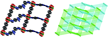
Single-crystal X-ray diffraction analysis shows that CP 1 crystallizes in the monoclinic space group C2/c (Table 1). In CP 1, the asymmetric unit contains two Zn(II) ions, one L, two bpca2−, two uncoordinated DMF molecules and 4.5 uncoordinated water molecules. The coordination environment of Zn(II) ion is shown in Fig. 1a. The crystallographically independent Zn(1) iron is five coordinated by one N atom from L and four O atoms from four bpca2− ligands in an distorted square-pyramidal coordination geometry [Zn–O = 2.025(2)–2.038(2) Å and Zn–N = 2.009(3) Å; Table 2]. The bond angles around the central Zn(1) ion range from 86.74(11)° to 163.36(11)° (Table 2). The Zn(2) ion is also five coordinated by one N from L and four O atoms from four L′2− ligands in an square-pyramidal coordination geometry [Zn–O = 2.027(2)–2.058(2) Å and Zn–N = 2.009(3) Å; Table 2]. The bond angles around the central Zn(2) ion range from 86.09(12)° to 162.87(11)° (Table 2). The crystallographically independent bpca2− ligand show a bis-bidentate coordination mode, and two Zn(II) ions are linked by four carboxylate groups from two bpca2− to form a Zn2 unit with a Zn⋯Zn separation of 2.9598 (6) Å (Fig. 1b). Different Zn2 units are further connected by bpca2− ligand into a one-dimensional (1D) chain (Fig. 1b). Herein, L ligand also acts as a μ2-bridge to connect two Zn(II) ions via its two terminal imidazole N atoms (Fig. 1c). If the Zn2 unit is considered as a node, it is connected to six neighboring Zn2 units through four bpca2− and two L ligands, thus the Zn2 unit can be considered as a 6-connnected node with a Schläfli symbol of (412·63). The bpca2− and L ligands both function as 2-connected linkers and they are not counted as nodes topologically,13 thus CP 1 shows a uninodal 6-connected three-dimensional (3D) framework with {412·63}-pcu topology (Fig. 1d).14 And 2-fold interpenetration is observed in the structure of CP 1 (Fig. 1d).13 The solvent-accessible volume of the unit cell of CP 1 is 12[thin space (1/6-em)]527.7 Å3, which is approximately 64.5% of the unit-cell volume (19[thin space (1/6-em)]409.0 Å3).15
image file: c6ra11641h-f1.tif
Fig. 1 Coordination environment of Zn(II) ions in CP 1 (Solvent molecules and H atoms omitted for clarity, atom with additional label A refer to the symmetry operation: x + 1/2, −y + 1/2, z + 1/2, 50% probability ellipsoids) (a); 1D chain consisting of Zn(II) and bpca2− in CP 1 (H atoms omitted for clarity) (b); 3D architecture of CP 1 constructed by Zn2 unit, bpca2− and L (solvent molecules and H atoms omitted for clarity) (c); schematic illustrating the 2-fold interpenetrated 3D framework with {412·63}-pcu topology in CP 1 (d).

Crystal structure of Cd2L2(4,4′-cdba)2·2DMF (2)

CP 2 crystallizes in the triclinic space group P[1 with combining macron] (Table 1). The asymmetric unit contains one Cd(II) ion, one L, one 4,4′-cdba2−, and two uncoordinated DMF molecules. The crystallographically independent Cd(1) ion is seven coordinated by two N atoms from two L ligands and five O atoms from three 4,4′-cdba2− ligands (Cd–O = 2.305(4)–2.535(4), Cd–N = 2.279(5)–2.281(5) Å), exhibiting an pentagonal bipyramid coordination geometry (Fig. 2a and Table 2). As shown in Fig. 2b, the 4,4′-cdba2− ligand shows a tridentate coordination mode linking three Cd(II) ions with one chelating/bridging and one chelating carboxylate groups. Two Cd(II) centers are connected by the carboxylate groups from 4,4′-cdba2− ligands into a Cd2 unit with a Cd⋯Cd separation of 3.943 Å, which is further linked by two strands of 4,4′-cdba2−-bridges into 1D chain (Fig. 2b). In CP 2, the crystallographically independent L ligand also acts as a μ2-bridge to connect two Cd(II) centers via its two terminal imidazole N atoms (Fig. 2c). In CP 2, each Cd2 unit is connected to four neighboring Cd2 units through two double strands of 4,4′-cdba2−-bridges and two double strands of L ligands, thus it can be defined as a 4-connnected node. The 4,4′-cdba2− and L ligands both act as 2-connected linkers and they are not counted as nodes topologically,13 thus CP 2 displays a uninodal 4-connected two-dimensional (2D) layer with 44-sql topology (Fig. 2d).14 The solvent-accessible volume of the unit cell of CP 2 is 879.6 Å3, which is approximately 38.9% of the unit-cell volume (2259.7 Å3)15 and much smaller than the solvent-accessible volume in CP 1.
image file: c6ra11641h-f2.tif
Fig. 2 Coordination environment of Cd(II) ions in CP 2 (Solvent molecules and H atoms omitted for clarity, atom with additional labels refer to the symmetry operations: (A) x, y − 1, z − 1; (B) 1 − x, −y, 1 − z; (C) 1 + x, −1 + y, z, 50% probability ellipsoids) (a); 1D chain consisting of Cd(II) and 4,4′-cdba2− ligands in CP 2 (H atoms omitted for clarity) (b); 2D framework of CP 2 (Solvent molecules and H atoms omitted for clarity) (c); schematic illustrating the 44-sql topology of CP 2 (d).

Thermal stability

The phase purities of CPs 1 and 2 were supported by the powder X-ray diffraction (XRD) patterns of the samples, which are consistent with the calculated patterns (Fig. S3). The thermal stabilities of the CPs 1 and 2 were measured by thermogravimetric analyses (TGA) (Fig. S4). The samples were heated up to 700 °C in nitrogen atmosphere. The TGA curve of CP 1 reveals an initial weight loss of 9.1% from 25 to 300 °C corresponding to the removal of the uncoordinated DMF and H2O molecule (calcd 9.7%) (Fig. S4a). The decomposition of the framework of CP 1 began at 350 °C (Fig. S4a). As shown in Fig. S4b, CP 2 shows the first step of weight loss of 10.0% in the range of 25–300 °C, consistent with the loss of two uncoordinated DMF molecule (calc. 9.9 wt%). Decomposition of the structure of CP 2 began at 350 °C (Fig. S4b).

Electrochemical properties of CPs 1 and 2

In order to examine the electrochemical properties of CPs 1 and 2, cyclic voltammetry studies were carried out in a three-electrode test cell with a saturated calomel electrode (SCE) and a Pt foil as the reference and counter electrode, respectively. Fig. 3 is the cyclic voltammograms (CVs) of CP 1-modified electrode (1-GCE) and CP 2-modified electrode (2-GCE) in 0.05 M KH2PO4/NaOH aqueous solution (pH = 6.8) in the range from −1.5 to 1.5 V vs. SCE. As observed in Fig. 3 and S5, 1-GCE displays a reversible redox couple with Epa = −1.1 V (Epa, anodic peak potential) and Epc = −1.3 V (Epc, cathodic peak potential) vs. SCE in the potential range from −1.5 to +1.5 V at a scan rate of 0.005 V s−1, which may be related with the redox of the Zn(II) in CP 1. The peak-to-peak separation between the anodic and cathodic (ΔEp) is 0.2 V. When 2-GCE is used, a reversible redox couple is observed with Epa = −0.80 V and Epc = −1.0 V vs. SCE at 0.005 V s−1, which may be related with the redox of the Cd(II) in CP 2 (Fig. 3 and S6). The peak-to-peak separation between the anodic and cathodic (ΔEp) is 0.20 V. As for 1-GCE and 2-GCE, similar irreversible peak is observed at −0.36 V vs. SCE in the potential range from −1.5 to +1.5 V at a scan rate of 0.005 V s−1, it is probably related with the impurity of the bare GCE though the GCE has been polished and washed completely.
image file: c6ra11641h-f3.tif
Fig. 3 Cyclic voltammograms (CVs) of 1-GCE (blue) and 2-GCE (red) in 0.05 M KH2PO4–NaOH aqueous solution (pH = 6.8) at a sweep rate of 0.005 V s−1.

UV-vis absorption and diffuse reflectance spectra of CPs 1 and 2

In order to investigate the charge-transfer mechanism of the two CPs, the UV-vis absorption and diffuse reflectance spectra of the two CPs were carried out at room temperature. As shown in Fig. S7, L exhibit strong absorption with maxima at 257 and 314 nm in the range of 250–450 nm, respectively, which may be ascribed to the n–π* or π–π* transition (Fig. S7).16 CPs 1 and 2 display absorption peaks at 267 and 264 nm in the range of 240–500 nm, respectively (Fig. S7). The UV-vis absorption spectra for CPs 1 and 2 are different from those of the free organic ligand, indicating that they may be ascribed to the intraligand charge-transfer transition (ILCT), ligand-to-ligand charge-transfer transition (LLCT) or metal ion-involved charge-transfer transition.17

The diffuse reflectance spectra of the samples are shown in Fig. S8. According to the plot of the reflectance versus the radiation energy, the band gaps of CPs 1 and 2 are calculated as ca. 2.7 and 2.3 eV, respectively (the band-gap extraction method was elaborated in the ESI).17 As described above, CP 1 is constructed by Zn(II), L and bpca2−, whereas CP 2 is built up by Cd(II), L and 4,4′-cdba2−. The two CPs possess different band gaps, which is due to their different compositions and frameworks.

From the onset of oxidation peaks in the cyclic voltammograms (Fig. 3 and S5), the HOMO energy level of CP 1 can be calculated as −3.40 eV vs. vacuum. As discussed above, the absorption edges of CPs 1 and 2 suggest the HOMO-LUMO gaps of 2.7 eV and 2.3 eV, respectively (Fig. S8). On the basis of the energy gap and the HOMO energy level, the LUMO energy level of CP 1 can be calculated as 2.7 + (−3.40) = −0.70 eV vs. vacuum.

Similarly, the HOMO energy level of CP 2 is estimated to be −3.68 eV vs. vacuum (Fig. 3 and S6). And the LUMO energy level of the CP 2 is calculated as 2.3 + (−3.68) = −1.38 eV vs. vacuum.

Band structure and orbital calculations of CPs 1 and 2

In order to verify the experiment result, the band structures, the total (TDOS) and partial density of states (PDOS) of the two CPs were calculated by CASTEP program. Herein, in order to simply the calculation, the uncoordinated DMF molecules were removed from the single crystal structural data of CP 1 for the calculation. The band structures of the desolvated CP 1 and CP 2 near the Femi energy level calculated by CASTEP program are shown in Fig. 4a and b, respectively. As shown in Fig. 4a and b, the bands in the valence band (VB) as well as in the conduction band (CB) are very flat and with very small dispersion, which is the common feature for MOFs materials.15 The gap between the lowest energy of the CB and the highest energy of the VB is about 2.789 eV for CP 1 and 2.417 eV for CP 2, indicating the band gaps of the two CPs are similar (Fig. 4 and Table 3). However, the two CPs possess totally different band structures.
image file: c6ra11641h-f4.tif
Fig. 4 Band structures of CPs 1 (a) and 2 (b).
Table 3 Band Structures of CPs 1–2
  CP 1 CP 2
The CB minimum vs. Fermi level (eV) 0.143 1.605
The VB maximum vs. Fermi level (eV) −2.646 −0.812
Band gap (eV) 2.789 2.417


As shown in Fig. 4a and Table 3, it can be found that the lowest energy (0.143 eV) of CB and the VB maximum (−2.646 eV) for CP 1 are located at points M and A, respectively, which confirms that CP 1 has an indirect band gap. CP 2 also shows an indirect optical band gap but with its CB minimum (1.605 eV) and VB maximum (−0.812 eV) locating at points Z and F, respectively (Fig. 4b and Table 3). As shown in Fig. 4a, it is further found the CB minimum (0.143 eV) of CP 1 is in the vicinity of its Fermi level (0 eV), indicating the n-type character of CP 1. However, the VB maximum (−0.812 eV) of CP 2 locates in the vicinity of its Fermi level (0 eV), indicating CP 2 is a p-type semiconductor (Fig. 4b).

Fig. 5a and b shows the TDOS and PDOS of the desolvated CP 1 and CP 2, respectively. As shown in Fig. 5a and b, it is found that the PDOS of the H atoms have no contribution to the bottom of the CB of both CPs 1 and 2. The bottom of the CB in CP 1 is mainly composed of C 2p, N 2p and O 2p states (Fig. 5a), whereas in CP 2, it is dominated by C 2p and O 2p states (Fig. 5b). As described above, CPs 1 and 2 exhibit different 3D and 2D frameworks, respectively, which gives rise to the different compositions of the bottom of the CB in the two CPs, then lead to their different CB minima (0.143 eV for CP 1 and 1.605 eV for CP 2).


image file: c6ra11641h-f5.tif
Fig. 5 TDOS and PDOS of CPs 1 (a) and 2 (b). In the PDOS, blue, red and green lines represent s, p and d orbits, respectively.

As shown in Fig. 5a and b, it is noted that the PDOS of the H atom does not influence the top of the VB in CP 1, whereas it has contribution to the top of the VB in CP 2. The top of the VB in CP 1 is composed of Zn 3d, O 2p, C 2p and N 2p states (Fig. 5a), and the top of the VB in CP 2 is dominated by Cd 3d, O 2p, C 2p, N 2p and H 1s states (Fig. 5b). As discussed above, Zn2 and Cd2 units are observed in the two CPs, respectively, indicating the metal(II) centers in the CPs have important contribution to the top of the VB, thus giving rise to their different VB maxima (−2.646 eV for CP 1 and −0.812 eV for CP 2).

Photoelectrochemical behaviors of the samples

In order to investigate the photocurrent responses of the samples, the photoelectrochemical tests were carried out at room temperature. The photoelectrochemical tests were performed using an electrochemical workstation (CHI660E) in a three-electrode set-up with a platinum plate (1 × 2 cm2) and a Ag/AgCl as the counter and reference electrodes, respectively.18 The photocurrent responses for all of the samples in 0.05 M KH2PO4/NaOH aqueous solution (pH = 6.8) at bias potential of 0 V vs. Ag/AgCl under the illumination from a 300 W Xe arc lamp (650 nm > λ > 350 nm) (the active area of electrode is 1 cm−2) are shown in Fig. 6.
image file: c6ra11641h-f6.tif
Fig. 6 Photocurrent responses on different samples under chopped visible light irradiation (650 nm > λ > 350 nm) at 110 mW cm−2 with the vertical axis denoted in different scales (a) and (b).

As shown in Fig. 6a and S9a, CP 1 yielded the photocurrent density of ca. 4 × 10⁻⁶ mA cm−2 when the irradiation was switched on. Obviously, the photocurrent density on CP 2 (1.4 × 10⁻⁵ mA cm−2) is 3.5 times than that on CP 1 (4 × 10⁻⁶ mA cm−2) (Fig. S9b). Herein, the order of photocurrent densities was CP 2 > CP 1, which follows the reverse order of their band gaps. On the other hand, the HOMO energy level of CP 2 (−3.68 eV) is lower than that of CP 1 (−3.40 eV), furthermore, the LUMO energy of CP 2 (−1.38 eV) is not higher than that of CP 1 (−0.70 eV) (Fig. 7), indicating the electrons from the HOMO of CP 2 are more easily excited and injected into the LUMO of CP 2 in comparison with the electrons from CP 1, therefore, CP 2 produces larger current density than CP 1.


image file: c6ra11641h-f7.tif
Fig. 7 Energy level diagram of CPs 1 and 2.

As shown in Fig. 6a and b, steady photocurrents with rapid responses were observed for CP 1, CdTe and the CP 1@CdTe composite when they were illuminated by visible light (650 nm > λ > 350 nm) and the decay was negligible after several on/off cycles of illumination.

As shown in Fig. 6a and b and S9a, the photocurrent density on CP 1 is 4 × 10⁻⁶ mA cm−2, which almost can be neglected with respect to the photocurrent density observed on CdTe (4 × 10⁻⁴ mA cm−2) (Fig. 6b and S9a). And the photocurrent density was significantly increased on the CP 1@CdTe-modified ITO electrode (4.6 × 10⁻⁴ mA cm−2) (Fig. 6b and S9a). The photocurrent density on CP 1@CdTe (4.6 × 10⁻⁴ mA cm−2) is 115 times on CP 1 (4 × 10⁻⁶ mA cm−2) and 1.15 times on CdTe (4 × 10⁻⁴ mA cm−2), respectively, indicating the CP 1@CdTe composite exhibits much higher photocurrent density than both CP 1 and CdTe. This enhancement on the photocurrent density suggested the higher separation efficiency of the photogenerated charge carriers on the CP 1@CdTe composite with respect to CP 1 and CdTe.

The energy levels of CP 1 and CdTe were displayed in Fig. 8.19 As shown in Fig. 8, CdTe possesses much narrow band gap (1.5 eV) than that of CP 1 (2.7 eV) with its HOMO (−5.23 eV) and LUMO energies (−3.75 eV) both lower than the HOMO (−3.40 eV) and LUMO (−0.70 eV) energies of CP 1,19 indicating it is more easily for the electrons from the HOMO of CdTe to be excited into the LUMO of CdTe with respect to the electrons from the HOMO of CP 1, thus CdTe possesses much better photovoltaic property than CP 1, which is in agreement with our experiment result.


image file: c6ra11641h-f8.tif
Fig. 8 Energy level diagram of CP 1 and CdTe.

When the CP 1@CdTe composite was irradiated by the visible light (650 nm > λ > 350 nm), the energy absorbed by CdTe caused the excitation of electrons from the HOMO of CdTe into the LUMO of CdTe (Fig. 8). However, herein, the energy of the visible light (650 nm > λ > 350 nm, 3.5 eV > energy > 1.9 eV) is larger than the band gap of CdTe (1.5 eV), and the HOMO of CP 1 is −3.40 eV, which is near the LUMO of CdTe (−3.75 eV) (Fig. 8). Then it is expected that the photoinduced electrons of the LUMO of CdTe can be further transferred into the HOMO of CP 1 due to their matched energy levels to prevent the photoinduced charge recombination of CdTe (Fig. 8). Consequently, the CP 1@CdTe composite exhibits higher photocurrent density than both CdTe and CP 1.

Electrochemical impedance spectra (EIS) of CPs 1 and 2

The photoinduced charge transfer process in a semiconductor can be monitored by the electrochemical impedance spectra (EIS).20 The radius of the arc in the high frequency region of the Nyquist plot indicates the impedance of the charge transfer on the surface of electrode, and the smaller radius of the arc suggests the smaller impedance of charge transfer and the higher efficiency of charge transfer. Fig. S10 displays the Nyquist plots of the samples with and without visible light irradiation (650 nm > λ > 350 nm). And the arc radii of all the samples with illumination are smaller than those without illumination, indicating that visible light irradiation can promote the charge transfer process.

As shown in Fig. S10a, the arc radius in the Nyquist plot of CP 2 is smaller than that in the Nyquist plot of CP 1 both with and without illumination, indicating the higher efficiency of charge transfer in the presence of CP 2 than in the presence of CP 1, thus CP 2 shows enhanced photocurrent response than CP 1. It also can be seen that the arc radius in the Nyquist plot of the CP 1@CdTe composite is smaller than those in the Nyquist plots of CP 1 and CdTe in the cases of with and without illumination (Fig. S10b), indicating the highest efficiency of charge transfer in the presence of the CP 1@CdTe composite with respect to CdTe and CP 1, which is probably associated with the prevention of the charge recombination to some extents in the coexistence of CdTe and CP 1.

To further reveal the mechanism for the photocurrent production, the Mott–Schottky curves of the CPs-modified ITO electrodes were measured.21 As shown in Fig. S11a, it is found the Mott–Schottky plot of CP 1-modified electrode in the dark show a linear relationship in the range of −0.4–0 V vs. Normal Hydrogen Electrode (NHE) for C−2 versus E with a positive slope, which indicate that CP 1 is n-type semiconductor, which is in agreement with its band structure calculation (Fig. 4a). And the negative slope of the Mott–Schottky plot for CP 2 indicates the p-type behavior of the CP (Fig. S11b), which is consistent with its band structure analysis (Fig. 4b).

Conclusion

In conclusion, based on a rigid N donor, 3-(3-(1H-imidazol-1-yl)phenyl)-5-(4-(1H-imidazol-1-yl)phenyl)-1-methyl-1H-1,2,4-triazole(L) and two multicarboxylate ligands, two metal(II)-based CPs formulated as Zn4L2(bpca)4·4DMF·9H2O (H2L′ = biphenyl-4,4′-dicarboxylic acid) (1) and Cd2L2(4,4′-cdba)2·2DMF (4,4′-H2cdba = 4,4′-carbonyldibenzoic acid) (2) were synthesized under solvothermal conditions and structurally characterized by single-crystal X-ray diffraction. CP 1 is a 2-fold interpenetrated uninodal 6-connected 3D framework with a {412·63}-pcu topology. CP 2 displays a uninodal 4-connected 2D layer with a 44-sql topology. The two CPs exhibit different electrochemical and photoelectrochemical properties due to their different structures and band structures. CP 2 yielded the larger photocurrent density than CP 1, which is because the band gap of CP 2 is smaller than that of CP 1. Meanwhile, CdTe and the CP 1@CdTe composite have been synthesized by electrodeposition and characterized by powder XRD, SEM and energy dispersive spectroscopy (EDS) mapping. The CP 1@CdTe composite exhibits higher photocurrent density than CP 1 and CdTe, which is probably due to the matched energy levels of CdTe and CP 1, then leading to the prevention of photoinduced charge recombination to some extents. The Mott–Schottky plots reveal that CP 1 is a n-type semiconductor, and CP 2 is a p-type semiconductor. Investigation on the detailed mechanism is under way.

Acknowledgements

Financial supports from the National Natural Science Foundation of China (No. 21371184), the large-scale instrument and equipment open foundation in Chongqing University (No. 201606150053), Chongqing Key Laboratory of Chemical Process for Clean Energy and Resource Utilization and the Science and Technology Research Foundation of the Education Commission of Chongqing (KJ1501124) are gratefully acknowledged.

Notes and references

  1. (a) S. Leininger, B. Olenyuk and P. J. Stang, Chem. Rev., 2000, 100, 853 CrossRef CAS PubMed; (b) P. J. Steel, Acc. Chem. Res., 2005, 38, 243 CrossRef CAS PubMed; (c) C. Janiak, Coord. Chem. Rev., 2006, 250, 66 CrossRef CAS; (d) W. Y. Wong and C. L. Ho, Coord. Chem. Rev., 2006, 250, 2627 CrossRef CAS; (e) C. Wang, D. Liu and W. B. Lin, J. Am. Chem. Soc., 2013, 135, 13222 CrossRef CAS PubMed.
  2. T. Osawa, T. Kajitani, D. Hashizume, H. Ohsumi, S. Sasaki, M. Takata, Y. Koizumi, A. Saeki, S. Seki, T. Fukushima and T. Aida, Angew. Chem., Int. Ed., 2012, 51, 7990 CrossRef CAS PubMed.
  3. (a) N. Stock and S. Biswas, Chem. Rev., 2012, 112, 933 CrossRef CAS PubMed; (b) C. Lu, T. Ben, S. Xu and S. Qiu, Angew. Chem., Int. Ed., 2014, 53, 6454 CrossRef CAS PubMed.
  4. (a) J. Xiang, C. L. Ho and W. Y. Wong, Polym. Chem., 2015, 6, 6905 RSC; (b) J. R. Li, Y. Ma, M. C. McCarthy, J. Sculley, J. Yu, H. K. Jeong, P. B. Balbuena and H. C. Zhou, Coord. Chem. Rev., 2011, 255, 1791 CrossRef CAS; (c) C. L. Ho and W. Y. Wong, Coord. Chem. Rev., 2013, 257, 1614 CrossRef CAS; (d) W. Y. Wong, Dalton Trans., 2007, 4495 RSC.
  5. (a) L. X. Xie, X. W. Hou, Y. T. Fan and H. W. Hou, Cryst. Growth Des., 2012, 12, 1282 CrossRef CAS; (b) Z. G. Gu, Y. T. Liu, X. J. Hong, Q. G. Zhan, Z. P. Zheng, S. R. Zheng, W. S. Li, S. J. Hu and Y. P. Cai, Cryst. Growth Des., 2012, 12, 2178 CrossRef CAS; (c) D. Y. Lee, E. K. Kim, N. K. Shrestha, D. W. Boukhvalov, J. K. Lee and S. H. Han, ACS Appl. Mater. Interfaces, 2015, 7, 18501 CrossRef CAS PubMed; (d) C. H. Hendon, D. Tiana and A. Walsh, Phys. Chem. Chem. Phys., 2012, 14, 13120 RSC; (e) D. Y. Lee, I. Lim, C. Y. Shin, S. A. Patil, W. Lee, N. K. Shrestha, J. K. Lee and S. H. Han, J. Mater. Chem. A, 2015, 3, 22669 RSC; (f) D. K. Lee, C. Y. Shin, S. J. Yoon, H. Y. Lee, W. Lee, N. K. Shrestha, J. K. Lee and S. H. Han, Sci. Rep., 2014, 4, 3930 Search PubMed.
  6. (a) X. X. Yan, X. D. Qiu, Z. S. Yan, H. J. Li, Y. Gong and J. H. Lin, J. Solid State Chem., 2016, 237, 313 CrossRef CAS; (b) P. Zhang, Y. Gong and J. H. Lin, Eur. J. Inorg. Chem., 2016, 3, 322 CrossRef.
  7. P. Zhang, X. Yang, P. G. Jiang, J. L. Yin, Y. Gong and J. H. Lin, RSC Adv., 2015, 5, 34058 RSC.
  8. (a) Z. H. Huang, G. Q. Liu and F. Y. Kang, ACS Appl. Mater. Interfaces, 2012, 4, 4942 CrossRef CAS PubMed; (b) C. Wang, Z. Xie, K. E. deKrafft and W. B. Lin, J. Am. Chem. Soc., 2011, 133, 13445 CAS; (c) M. Martis, K. Mori, K. Fujiwara, W. Ahn and H. Yamashita, J. Phys. Chem. C, 2013, 117, 22805 CrossRef CAS.
  9. (a) S. D. Gunjal, Y. B. Khollam, S. R. Jadkar, T. Shripathi, V. G. Sathe, P. N. Shelke, M. G. Takwale and K. C. Mohite, Sol. Energy, 2014, 106, 56 CrossRef CAS; (b) D. Banga, B. Perdue and J. Stickney, J. Electroanal. Chem., 2014, 716, 129 CrossRef CAS; (c) H. Gómez, R. Henríquez, R. Schrebler, G. Riveros, D. Leinen, J. R. Ramos-Barrado and E. A. Dalchiele, J. Electroanal. Chem., 2004, 574, 113 CrossRef; (d) İ. Şişman and Ü. Demir, J. Electroanal. Chem., 2011, 651, 222 CrossRef; (e) S. Chander and M. S. Dhaka, Physica E, 2015, 73, 35 CrossRef CAS; (f) K. R. Chauhan, I. J. Burgess, G. S. Chang and I. Mukhopadhyay, J. Electroanal. Chem., 2014, 713, 70 CrossRef CAS; (g) B. Shan, W. Wu, K. Feng and H. Nan, Mater. Lett., 2016, 166, 85 CrossRef CAS.
  10. (a) G. M. Sheldrick, SHELXS 97, Program for Crystal Structure Solution, University of Göttingen, Göttingen, Germany, 1997 Search PubMed; (b) G. M. Sheldrick, SHELXL 97, Program for Crystal Structure Refinement, University of Göttingen, Göttingen, Germany, 1997 Search PubMed.
  11. (a) A. L. Spek, J. Appl. Crystallogr., 2003, 36, 7 CrossRef CAS; (b) X. F. Wang, Y. B. Zhang, H. Huang, J. P. Zhang and X. M. Chen, Cryst. Growth Des., 2008, 8, 4559 CrossRef CAS.
  12. B. Fang, C. H. Zhou and X. C. Rao, Eur. J. Med. Chem., 2010, 45, 4388 CrossRef CAS PubMed.
  13. O. D. Friedrichs, M. O'Keeffe and O. M. Yaghi, Acta Crystallogr., Sect. A: Found. Crystallogr., 2003, 59, 22 CrossRef.
  14. V. A. Blatov, IUCr CompComm. Newsletter, 2006, 7, 4 Search PubMed.
  15. A. L. Spek, Acta Crystallogr., Sect. A: Found. Crystallogr., 1990, 46, C34 Search PubMed . The free water molecules were removed before the cited solvent accessible volume was calculated by PLATON.
  16. (a) S. Ohkoshi, H. Tokoro, T. Hozumi, Y. Zhang, K. Hashimoto, C. Mathonière, I. Bord, G. Rombaut, M. Verelst, C. C. Moulin and F. Villain, J. Am. Chem. Soc., 2006, 128, 270 CrossRef CAS PubMed; (b) J. H. Wang, Y. Q. Fang, L. Bourget-Merle, M. I. J. Polson, G. S. Hanan, A. Juris, F. Loiseau and S. Campagna, Chem.–Eur. J., 2006, 12, 8539 CrossRef CAS PubMed; (c) D. D. Censo, S. Fantacci, F. D. Angelis, C. Klein, N. Evans, K. Kalyanasundaram, H. J. Bolink, M. Grätzel and M. K. Nazeeruddin, Inorg. Chem., 2008, 47, 980 CrossRef PubMed.
  17. (a) B. C. Tzeng, T. H. Chiu, B. S. Chen and G. H. Lee, Chem.–Eur. J., 2008, 14, 5237 CrossRef CAS PubMed; (b) S. Chavan, J. G. Vitillo, E. Groppo, F. Bonino, C. Lamberti, P. D. C. Dietzel and S. Bordiga, J. Phys. Chem. C, 2009, 113, 3292 CrossRef CAS; (c) Q. Wang, J. E. Moser and M. Grätzel, J. Phys. Chem. B, 2005, 109, 14945 CAS; (d) M. K. Datta, K. Kadakia, O. I. Velikokhatnyi, P. H. Jampani, S. J. Chung, J. A. Poston, A. Manivannan and P. N. Kumta, J. Mater. Chem. A, 2013, 1, 4026 RSC; (e) R. N. Reddy and R. G. Reddy, J. Power Sources, 2004, 132, 315 CrossRef CAS; (f) S. Ghosh, R. K. Sahu and C. R. Raj, J. Mater. Chem., 2011, 21, 11973 RSC.
  18. K. Gelderman, L. Lee and S. W. Donne, J. Chem. Educ., 2007, 84, 685 CrossRef CAS.
  19. Q. S. Zeng, Z. L. Chen, Y. Zhao, X. H. Du, F. Y. Liu, G. Jin, F. X. Dong, H. Zhang and B. Yang, ACS Appl. Mater. Interfaces, 2015, 7, 23223 CAS.
  20. Y. L. Zheng, D. L. Liu, S. W. Liu, S. Y. Xu, Y. Z. Yuan and L. Xiong, J. Environ. Sci., 2009, 21, 1194 CrossRef CAS.
  21. (a) K. Gelderman, L. Lee and S. W. Donne, J. Chem. Educ., 2007, 84, 685 CrossRef CAS; (b) M. S. Prévot, Y. Li, N. Guijarro and K. Sivula, J. Mater. Chem. A, 2016, 4, 3018 RSC; (c) S. Eslava, L. P. Zhang, S. Esconjauregui, J. W. Yang, K. Vanstreels, M. R. Baklanov and E. Saiz, Chem. Mater., 2013, 25, 27 CrossRef CAS; (d) W. Zhang, Y. Cai, R. G. Xiong, H. Yoshikawa and K. Awaga, Angew. Chem., Int. Ed., 2010, 49, 6608 CrossRef CAS PubMed.

Footnote

Electronic supplementary information (ESI) available: Crystallographic data; SEM images; energy dispersive spectroscopy (EDS) mapping; PXRD patterns; TG curves; CVs; UV-vis absorption and diffuse reflectance spectra; photocurrent responses; Nyquist plots; Mott–Schottky curves; gas sorption. CCDC 1435043 and 1435044. For ESI and crystallographic data in CIF or other electronic format see DOI: 10.1039/c6ra11641h

This journal is © The Royal Society of Chemistry 2016
Click here to see how this site uses Cookies. View our privacy policy here.