Systematic study on the impact of water on the performance and stability of perovskite solar cells†
Charlotte Clegg and
Ian G. Hill*
Dalhousie University, Department of Physics and Atmospheric Science, 6310 Coburg Rd., Halifax, Canada. E-mail: ian.hill@dal.ca; Fax: +902-494-5191; Tel: +902-494-3897
First published on 25th May 2016
Abstract
The effects of water on the photovoltaic performance of methylammonium lead iodide perovskite devices has recently become a topic of interest within the perovskite community. However, existing studies report contrasting and sometimes contradictory observations. In this work, small concentrations of water, consistent with those present in air-exposed DMF, were systematically incorporated directly into the PbI2 precursor solution in order to investigate its effect on the performance of sequentially spin-coated, inverted perovskite solar cells. Increasing concentrations of water in the PbI2 solution were found to have a negative impact on photovoltaic performance. The addition of water was observed to exaggerate the scan-rate and directional-dependent hysteresis and introduce new transient behaviours in comparison to the “dry” devices. Interestingly, the addition of water was also found to improve the long-term device stability in comparison with devices fabricated from “dry” precursors.
1 Introduction
Perovskite photovoltaics have rapidly risen to the forefront of next generation photovoltaic technologies. In just over five years, the power conversion efficiencies of methylammonium lead halide perovskites have improved from a modest 3%, to a certified 20.1%.1,2 The increased performance is owed largely to improvements in device architecture, film coverage and morphology. However, several unique properties, such as low exciton binding energies, low charge carrier recombination rates (and long carrier diffusion lengths) and the ability to absorb strongly across the visible spectrum, have made these materials promising candidates for next generation solar cells.3–6 Many groups have shown that high device efficiencies can be achieved using relatively simple low-temperature solution processing techniques, which can easily be applied to large-scale roll-to-roll manufacturing processes.7–13 Slot-die coated and inkjet printed perovskite devices have already achieved efficiencies in excess of 10%, a promising indicator for the commercial viability of this technology.14,15Despite such remarkable successes, perovskite photovoltaics are not without shortcoming. Methylammonium lead iodide perovskites are known to be extremely sensitive to water. Still, there is disagreement in the literature regarding the severity and reversibilty of water-induced degradation; and the exact degradation pathway(s) through which water interacts with the perovskite bulk remains unclear.16–23 Yang et al. systematically documented the degradation rates of perovskite films in controlled humidity environments via the formation of a hydrated intermediate.18 The degradation process was found to be at least partially reversible, which is similar to observations by Leguy et al., who documented the formation of a monohydrate perovskite phase upon exposure to a humid environment.19 Leguy et al. found that the hydrated perovskite demonstrated, approximately, a 90% reduction in the short circuit current density and 0.2 V decrease in the open circuit voltage; surprisingly, the authors reported complete reversibility after exposure to dry nitrogen for four hours. Conversely, Zhou et al. reported that a water vapour spray treatment of perovskite films resulted in improved crystallinity; the effect was found to be similarly reversible.24 Through similar investigations, many authors have shown that exposure to ambient water vapour is less detrimental to perovskites than previously thought. Indeed, exposure to ambient moisture during the precursor, deposition, annealing or post-fabrication stages can result in significant enhancements to the final device performance.25–29
Despite the growing interest in this new topic, several conflicting reports exist in the literature. Using a sequential spin coating procedure, Wu et al. report a dramatic improvement in the morphology of neat PbI2 films with the addition of 2 wt% H2O to the precursor solution. Their optimized fabrication procedure yielded an 18% efficient device in comparison with their control device, which achieved a maximum power conversion efficiency of 0.0063% using an anhydrous solution of PbI2.30 Also using a sequential deposition procedure, Adhikari et al. note that an optimized device performance and charge carrier lifetime are achieved with a concentration of 5 vol% H2O in the methylammonium iodide dipping solution.31 Conings et al. performed a similar study using a well documented mixed halide, single-step deposition procedure. They observed little overall change in device performance with the substitution of up to 10 vol% of the anhydrous DMF solvent with deionized H2O, suggesting that the required fabrication environment may be more flexible than previously thought.32 In contrast, Gong et al. report an enhancement in both photovoltaic performance and stability with the addition of 2 vol% H2O to the same single-step precursor solution.33 Such a wide variation in observations suggests that the effects of water on the morphology and performance of methylammonium lead halide devices are still not well understood; and, that more work is needed in order to elucidate the precise mechanism(s) through which water interacts with this unique material.
In this study, the effects of moisture on the photovoltaic performance and properties of perovskite devices were examined under highly controlled fabrication conditions. To minimize uncontrolled exposure to moisture, synthesis and testing of perovskite devices were all carried out in a dry, argon filled glovebox, save for the addition of controlled volumes of de-ionized water to the PbI2 solutions. It is well known that the morphology of the perovskite layer plays a critical role in the final device performance.34–36 Pinholes and film dewetting not only result in decreased absorbance by the perovskite layer, but also a greater number of recombination pathways (and consequently poorer device performance); therefore, the perovskite films in this study were fabricated via sequential spin-coating to reduce any effects that the contrasting solubility of the lead iodide (PbI2) and methylammonium iodide (MAI) precursors in water may have on film homogeneity.28
2 Experimental methods
2.1 Perovskite fabrication methods
2.2 Device characterization
Current density–voltage (JV) data were measured under simulated AM1.5G sunlight at 100 mW cm−2 using a ScienceTech solar simulator and a Keithley 236 source measure unit. The illumination intensity was calibrated using a calibrated silicon photodiode/KG5 glass filter combination. JV data were collected by sweeping from 1.5 V to −1.0 V (reverse scan) and −1.0 V to 1.5 V (forward scan) using two scanning rates: 1.0 V s−1 and 0.1 V s−1. Transient photocurrent measurements were performed by holding the device at 1.5 V for 2 seconds, then measuring the short circuit current density as a function of time for up to 500 seconds.2.3 Film characterization
Optical absorption measurements were collected with a Cary UV-vis spectrophotometer using a 300 nm min−1 scan rate. Steady state photoluminescence (PL) measurements were collected using a Cary Eclipse spectrophotometer; an excitation wavelength of 520 nm and 120 nm min−1 scan rate were used. A Phenom benchtop SEM was used to obtain scanning electron microscopy images of the perovskite films. A Siemens D5000 X-ray diffractometer was used to obtain structural information about the films. Patterns were collected by sweeping from a scattering angle of 2θ = 10–60° in 0.05° steps with a 5 s per step dwell time. The divergence, anti-scattering and receiving slits were 0.5°, 0.5°, and 0.1 mm, respectively. Separate films were fabricated for the XRD measurements to prevent degradation effects due to extended exposure to high energy X-ray irradiation in an ambient environment. Unless otherwise specified, all characterizations were performed in an ambient atmosphere, on glove-box stored films, within 24 hours of measuring the associated device (JV) performance.3 Results and discussion
3.1 Device performance
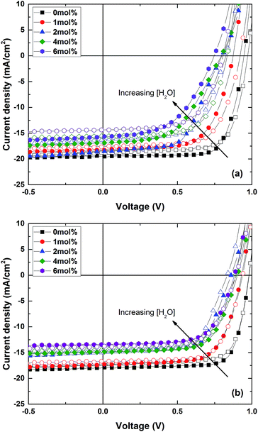
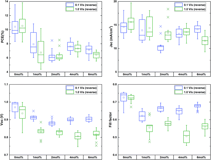
Fig. 1 compares the best devices achieved using varying concentrations of H2O in the PbI2 solution. A dramatic decrease in device performance is observed when increasing concentrations of water are added to the PbI2 precursor solution: the addition of 1 mol% of H2O results in a decreased open circuit voltage, by ∼100 mV, which is also accompanied by a minimum 10% decrease in the device fill factor. The loss of open circuit voltage and fill factor continues when the concentration of water in the PbI2 solution is further increased. When the water content is increased beyond 2 mol%, a drop in photocurrent, by up to ∼4 mA cm−2 is also observed. Together, these three trends have severely detrimental effects on overall device performance, as illustrated in Fig. 2 (a full tabulation of the average and best device performances under different scan rates is available in ESI Tables 1 and 2†).These trends are contrary to existing reports, where the addition of water is seen to either: yield a peak device performance using a specific concentration of water (Wu et al. and Gong et al.);30,33 or, produce no observable effect on morphology and overall device performance (Conings et al.).32 Conings et al. do note a similarly sustained drop in open circuit voltage with the addition of water to the perovskite precursor, but the effect is compensated by an increase in photocurrent, resulting in no change in the overall device performance. The variety of observations are difficult to resolve; however, the reported device fabrication procedures differ between each of the existing studies as well from the methods used in this study. As well, the added water may interact differently when used in different perovskite precursors (i.e.: single-step mixed halide solution in comparison to sequential spincoating of the two perovskite precursors). Currently, the only other studies to examine the impact of added water to sequentially deposited perovskite devices are less well-controlled, with all fabrication being performed in ambient conditions, where atmospheric water vapour may also contribute to the observed trends.30,31 We also highlight the superior performance of our control devices, and the fact that we have chosen to investigate the addition of much smaller volumes of water, with the belief that such volumes of water are more representative of those which may be inadvertently incorporated into the precursor during fabrication in air.
With respect to the anomalous hysteresis, which has been well-documented by many authors,40–43 very little was observed when the devices were measured using a 0.1 V s−1 scan rate. The JV data from the forward and reverse sweeps in Fig. 1 are nearly identical. This is further illustrated in Fig. S1,† which summarizes the batch statistics for several devices made using the same fabrication conditions; the difference between the reverse and forward scans is most reflected by a decreased open circuit voltage (up to ∼400 mV decrease) for devices with water added to the PbI2 solution. Scanning at 1.0 V s−1, resulted in a greater amount of hysteresis (Fig. 1 and S2†), which was exaggerated by further addition of H2O to the PbI2 solution. The lack of appreciable hysteresis in these devices is not surprising given that reduced hysteresis is often reported in inverted architecture perovskite devices.7,10,12,30,44,45 It has been suggested that the level of hysteresis is heavily influenced by particular charge selective contacts,45,46 where PCBM is additionally thought to passivate trap states within the perovskite that contribute to photocurrent hysteresis.47,48
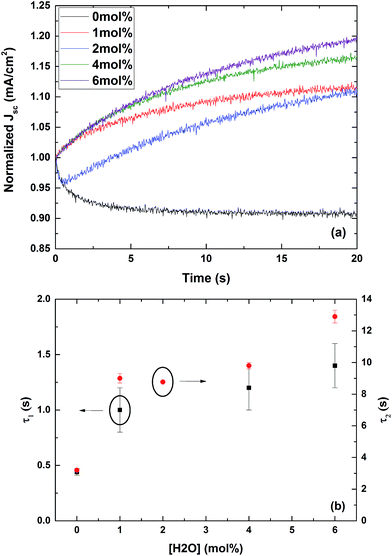
To further examine device hysteresis, the temporary enhancement by forward biasing (TEBBing, documented by O'Regan et al.) and its effect on the measured current density were measured.42 Each device was held at +1.5 V bias under 1 sun illumination for 2 seconds before measuring the short circuit current density over 20 seconds. Although strong evidence has been shown to suggest that bias history, and not light soaking, is responsible for hysteresis,42,43 each device was held at zero bias in the dark for 1 minute prior to measurement to minimize any possible contributions from competing light-driven effects, which have been suggested by other authors.40,49 The transient photocurrents measured over the 20 second period are shown in Fig. 3(a), normalized to their initial photocurrent (at t = 0 seconds). Interestingly, opposite dynamics were observed for devices made using dry precursors and devices made using “wet” precursors. The devices measured with no moisture added to the PbI2 solution exhibit a photocurrent decay. In contrast, all devices fabricated with added water experience a growth in photocurrent, which extends beyond the 20 second measurement period. As observed by other authors, the transient behaviour for each device is observed to be strongly biexponential;42,50 the time constants extracted from a biexponential fit to each of the transient behaviours are shown in Fig. 3(b). The slow time components of the photocurrent growth at 0 V are similar in magnitude to those reported by Eames et al. after holding a device in the dark at −0.5 V for 100 seconds. In this study, the magnitude of the time constants are seen to increase gradually with the included moisture content of the devices (Fig. 3(b)). An anomaly is observed in devices made using 2 mol% H2O in the PbI2 solution, which demonstrate an initial photocurrent decay, followed by monoexponential growth. Such behaviour suggests that two competing transport mechanisms may coexist within perovskite films.
The transient photocurrent measurements were repeated over a 500 second time scale, shown in Fig. 4. The reverse, then forward JV sweeps of the corresponding devices were also measured at various scan rates (1.0 V s−1, 0.1 V s−1, then 0.01 V s−1). Again, devices fabricated from a dry PbI2 solution were seen to exhibit a photocurrent decay; whereas, devices fabricated from “hydrated” precursors demonstrated a photocurrent growth with time. The steady state photocurrent observed in Fig. 4(a) nearly converges with the JV photocurrent measured from the same device at the slowest scan rate. As indicated by other authors this suggests that only very slow JV sweep rates (≤0.01 V s−1) are truly reflective of steady state device operation.40 Unexpectedly, the transient photocurrent growth observed in “hydrated” devices is not accompanied by an increased photocurrent at slower scan rates, but rather a decreased photocurrent and an increased open circuit voltage.
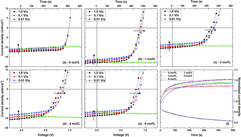 | ||
| Fig. 4 Rate dependent JV measurements (for reverse sweeps) and transient photocurrent behaviours for the corresponding devices with varying concentrations of H2O in the PbI2 solution, (a)–(e). The transient photocurrents are plotted in green, and correspond to the time axis from 0 to 500 seconds. The transients shown in (a)–(e) are contrasted in (f), normalized to the initial photocurrents. (The measurements shown in this figure were taken 20 days post-fabrication. Results from a biexponential fit to each transient photocurrent are summarized in the ESI†.) | ||
Transient behaviours and anomalous hysteresis are commonly suggested to result from the motion of ionic species within the perovskite layer: I−, MA+ and Pb2+.41,43,47,50–53 Although the suggested activation energy and migration time scale for each species varies between studies, I− consistently appears to exhibit the highest mobility, followed by MA+ and Pb2+.22,50–52 Shao et al. have also produced convincing experimental evidence linking I− migration with hysteresis.53
In the presence of water, H2O incorporation into the perovskite is thought to be energetically favourable, leading to its spontaneous infiltration into the lattice.22 Both computational and experimental studies suggest that the absorbed water interacts strongly with the methylammonium cation and surrounding iodine atoms through hydrogen-bonding;22 however, the ultimate degradation pathway(s) caused by water exposure are not agreed upon. Some authors propose an acid–base reaction, whereby a single water molecule may be sufficient to degrade the material, but an excess of water is required to dissolve the byproducts.16,54
| n[(CH3NH3+)PbI3] + H2O → [(CH3NH3+)n−1(CH3NH2)nPbI3][H3O] → HI + CH3NH2 + H2O + PbI2 + (n − 1)[(CH3NH3+)PbI3] | (1) |
Other authors suggest a reversible hydration of the perovskite, where irreversible degradation is only achieved if an excess of water is present to dissolve the CH3NH3+.18,19
| 4(CH3NH3)PbI3 + 4H2O ⇌ 4[CH3NH3PbI3·H2O] ⇌ (CH3NH3)4PbI6·2H2O + 3PbI2 + 2H2O | (2) |
Regardless of the exact degradation pathway, the addition of water in this study likely increased the population of mobile ions within the perovskite film, and may have changed the activation energy associated with the migration of each species. A larger number of mobile ionic species would explain the increased hysteresis observed when higher concentrations of water were included in the perovskite film. For the “dry” perovskite, the I− ions would migrate towards the device anode under the two-second forward bias treatment. Assuming that the transport of such species is restricted to motion within the perovskite layer, extended forward biasing would cause an accumulation of negative charge near the PEDOT/perovskite interface. This in turn would create an internal electric field, which would facilitate hole extraction. Once the device is short-circuited, the build-up of I− ions would be driven by a concentration gradient to diffuse away from the interface, resulting in a decreased charge collection efficiency over time and hence a decreased photocurrent (Fig. 4). This behaviour is also reflected in the sequence of JV sweeps presented in Fig. 4; reverse sweeps performed at slower scan rates would allow greater relaxation of the ionic concentration gradient, resulting in a decreased charge collection efficiency and, therefore, a lower photocurrent.
It is speculated that the addition of water may favour the motion of MA+ over I− ions. In pure monohydrate and dihydrate perovskite crystals, water is incorporated between the [PbI6]4− octahedra with the methylammonium cation, resulting in an arrangement of [PbI6]4− octahedra separated by methylammonium ions and H2O.19,23,55 Although no crystalline hydrate phases were observed in this study within the detection limits of XRD (Fig. 6), it is possible that sufficient water was incorporated into the perovskite lattice to disrupt the caging of the MA+ cation, and facilitate its migration through the film. Other authors have also suggested that the methylammonium cation is deprotonated in the presence of H2O,16,54 which could allow liberated H+ ions to migrate through the lattice and contribute to the transient photocurrent. The energy barrier for H+ migration is suggested to be lower than that for intrinsic ionic species such as CH3NH3+ and I−.50,56 This difference in energy barriers could account for the difference in transient dynamics observed between “dry” and “hydrated” devices. Under the two-second forward bias treatment, the mobile MA+ (and possibly H+) ions would migrate towards the device cathode, resulting in an accumulation of positive charge at the perovskite/PCBM interface. The accumulation of positive charge would create a localized potential well, trapping electrons and therefore decreasing the measured photocurrent. Once the device is short-circuited, the MA+ ions would diffuse away from the interface, allowing for more efficient charge collection over time. This behaviour is also reflected in the sequence of JV sweeps presented in Fig. 4 when considering the entire biasing history of the device. After the reverse sweep (+1.5 V to −1.0 V) at 1.0 V s−1, the device is immediately scanned in the forward direction (−1.0 V to +1.5 V) before it is again measured in the reverse direction (+1.5 V to −1.0 V) at 0.1 V s−1. Therefore, the most recent biasing history of the device before the reverse sweep at 0.1 V s−1 is 1.5 seconds at increasing forward bias, which results in positive ion accumulation at the perovskite/PCBM interface. The effect would be exaggerated for progressively slower scan rates; thus, the slowest scan rate (which was previously forward biased for the longest amount of time) should experience the largest photocurrent suppression. Although the suggested model of ion migration agrees well with experimental data, a more detailed investigation is necessary to verify these postulates and is currently underway.
3.2 Effect of water content on film morphology
Fig. 5 shows a series of top view SEM images for perovskite films fabricated with varying concentrations of water in the PbI2 solution and a dry (0 mol% H2O) MAI solution. In order, the images show perovskite films fabricated with 0 mol%, 1 mol%, 2 mol%, 4 mol% and 6 mol% H2O in the PbI2 solutions, respectively. The final image is of a PbI2 film with 0 mol% H2O, illustrating the high surface coverage of the PbI2 layer. Overall, the perovskite films appear to exhibit a compact, dense morphology and a high surface coverage. Films fabricated with less than 4 mol% H2O in the PbI2 solution exhibit higher surface coverage, with the majority of the grain sizes falling below 200 nm, and a small fraction of grains exceeding 500 nm in size. In contrast, a much higher fraction of grains are larger than 500 nm in films fabricated with 4 mol% and 6 mol% H2O in the PbI2 solutions, with some grains sizes even appearing to exceed 1 μm. These films, however, show a lower surface coverage with a significantly increased density of pinholes and cracking between larger grains (details are available in the ESI†). Similar trends regarding increased grain size and pinhole formation have also been reported in other studies where moisture is introduced during the perovskite fabrication procedure.26–29,32,33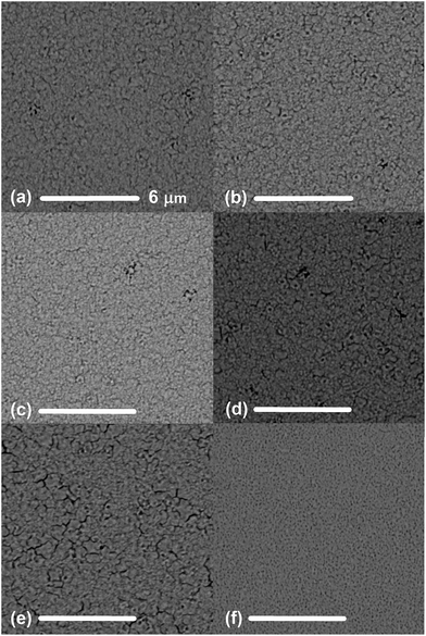 | ||
| Fig. 5 Top view SEM images of films made with varying concentrations of H2O in the PbI2 solution: (a) 0 mol%, (b) 1 mol%, (c) 2 mol%, (d) 4 mol% and (e) 6 mol%. A film of unconverted PbI2 with 0 mol% H2O is shown in (f). The scale bar represents 6 μm. Images were taken in regions corresponding to the device locations on the substrate (details are available in the ESI†). | ||
The observed trends in film morphology are congruent with trends observed in device performance. The increased cracking and pinhole formation in films with more moisture introduce a greater number of shunt pathways, which could explain the reduction in short circuit current and open circuit voltage for devices made with higher concentrations of water (Fig. 1 and 2). It is also possible that larger perovskite grain sizes could be accompanied by increased film roughening in the z-direction, leading to incomplete coverage by the PCBM layer and therefore greater recombination at the interface between the perovskite and the top contact.
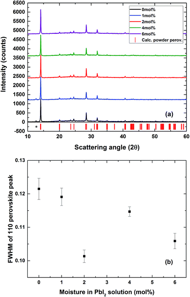
Fig. 6 shows a series of XRD patterns for films made with varying concentrations of H2O in the PbI2 solutions. The patterns indicate that the tetragonal (I4cm) MAIPbI3 perovskite phase was successfully formed in all instances with strong preferential orientation in the (110) direction, as is typical of spin coated MAIPbI3 thin films. All films are also seen to exhibit similar relative peak intensities. Interestingly, perovskite films fabricated with low concentrations of H2O in the PbI2 solution (0 mol% and 1 mol%) contain detectable amounts of crystalline PbI2, while the other films do not. Gangishetty et al., also observed incomplete conversion and residual crystalline PbI2 when sequential-step perovskite conversion was carried out in a low humidity environment (RH = 1%), while conversion under higher relative humidity was observed to yield phase pure perovskite.29 Whether the presence of the residual PbI2 peaks observed in this study is due to degradation during the annealing process, or simply due to incomplete conversion is unknown. As suggested by Gangishetty et al., it is possible that the presence of moisture may facilitate MAI incorporation into the PbI2/perovskite lattice by favouring the presence of a less-compact intermediate hydrate phase. It is also interesting to note that the higher performance of the 0 mol% and 1 mol% H2O devices corresponds to films with residual PbI2, which is consistent with the passivating effects of lead iodide suggested by other authors.57,58 Although these hypothesis are well-supported by the presented data (Fig. 5 and 6), it is important that the presence (or absence) of crystalline PbI2 in Fig. 6(a) be regarded with caution due to the inherent limitations of using the Bragg–Brentano diffraction geometry to indicate phase composition within a thin-film sample.
In this study, no significant enhancement in the diffraction intensity is observed with increasing moisture in the PbI2 solution. The fact that other studies have observed increased device performance and crystallinity in perovskite films that were annealed under high relative humidity suggests that the use of ambient moisture may act as a means of solvent vapour annealing.26 It is interesting to note that very similar effects to those reported in published moisture studies (that examine the effects of annealing treatments under controlled humidity environments) have also been observed in perovskite films treated with DMF solvent vapour.59 It therefore seems possible that the photophysical enhancements observed in such published reports may primarily be a consequence of morphological changes rather than any chemical changes resulting from the incorporation of water into the perovskite lattice.
Finally, although the Debye–Scherrer equation is typically only valid when analysing very small crystal sizes (<50 nm), the slight broadening of the (110) perovskite peak for films made with drier PbI2 (Fig. 6(b)) may be correlated with the higher proportion of smaller crystal sizes observed within the bulk of the “drier” perovskite films. The absence of unidentified peaks or diffraction signals at ∼8.7, 11.6 or 11.7° also suggests that no significant concentration of hydrated intermediates or precursors are present in our samples.18,19,60
3.3 Photophysics of the perovskite devices
Fig. 7 demonstrates the UV-vis absorption and photoluminescence spectra for perovskite films made with varying concentrations of H2O in the PbI2 solution. All of the films can be seen to exhibit similar absorption spectra, with no appreciable contribution from any residual lead iodide. The film made with no added water exhibits a nominally higher absorbance than the other films. In general, the absorption intensity of films is seen to decrease with increasing concentrations of water. However, it is difficult to ascertain whether this observation is a real trend, or merely a chance effect resulting from variations in scattered light between samples, or light transmission through cracks or pinholes. The characteristic perovskite PL emission is observed at ∼789 nm, with the highest intensity emission corresponding to the perovskite film made using dry precursor solutions. The intensity of the photoluminescent peak can be seen, generally, to decrease with the increasing addition of water to the lead precursor solution. This trend suggests an increased number of non-radiative recombination pathways, possibly due to an increased number of deep trap states, which would not be passivated by the PCBM layer.47,48 This is consistent with the decreased device performance observed in perovskite films with added moisture (Fig. 1). Leguy et al. link a decrease in device performance with the appearance of a hydrate phase after exposure to 77% relative humidity for 3 hours.19 Although no crystalline hydrate phase is observed in this study (Fig. 6), it is possible that the inclusion of water in the PbI2 precursor may have resulted in small quantities of a hydrated-perovskite phase dispersed throughout the film, which would act as recombination centres for photogenerated charge. Finally, peak fitting of the photoluminescent spectra reveals a slight blue shift (Δλ = ∼3 nm) in the peak luminescence wavelength with the addition of increasing quantities of water (Fig. 7(b), inset). Similar trends have been observed by other authors, where exposure of the perovskite to water is linked with a blueshifted PL spectrum.24,61 The observed blueshift is suggested to arise from lattice strain as water is incorporated into the perovskite crystal.22,61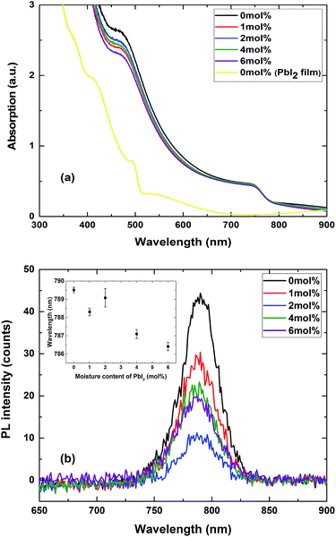 | ||
| Fig. 7 (a) UV-vis absorption and (b) photoluminescence spectra of films made with varying concentrations of H2O in the PbI2 solution, measured within 24 hours of device testing. | ||
3.4 Effect of moisture content on device stability
Remarkably, the inclusion of moisture into the perovskite layer via the PbI2 precursor is observed to have a stabilizing effect on device performance over time. Fig. 8 compares the JV curves for devices tested within 24 hours of fabrication with devices tested 20 days post-fabrication. The performance metrics are summarized in Table 1. All devices were stored under argon, and were at no point exposed to an ambient atmosphere. The best anhydrous device was observed to experience, roughly, a 25% decrease in power conversion efficiency and 30% decrease in photocurrent after 20 days storage under argon. The severity of the performance loss is alleviated by the inclusion of water in the PbI2 solution, with the best 1 mol% yielding the greatest stability and a higher PCE than the best dry device after 20 days. Only a 9% decrease in the measured power conversion efficiency was observed in the 1 mol% device after 20 days. Wu et al. and Gong et al. both report good device stabilities for their optimized devices in comparison to their control device, noting only a 10% and 8% reduction in PCE after 40 and 6 days, respectively.30,33 As far as we know, however, this is the first report where long-term device stability under inert conditions is explicitly linked to all devices with included moisture. In the context of this study, the stabilization mechanism enabled by the inclusion of H2O is unclear, but will be a topic of future investigation.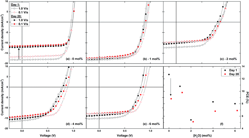 | ||
| Fig. 8 JV curves for devices with varying water concentrations measured 1 day (unshaded symbols) and 20 days (shaded symbols) post-fabrication. Two scan rates are shown (1.0 V s−1, black; and, 0.1 V s−1, red). The performance metrics for the 0.1 V s−1 scans on days 1 and 20 are presented in the final panel, and summarized in Table 1. | ||
| [H2O] (mol%) | Voc (V) | Jsc (mA cm−2) | PCE (%) | FF | ||||
|---|---|---|---|---|---|---|---|---|
| Day 1 | Day 20 | Day 1 | Day 20 | Day 1 | Day 20 | Day 1 | Day 20 | |
| 0 | 0.998 | 0.995 | 16.83 | 11.43 | 12.7 | 8.8 | 0.76 | 0.77 |
| 1 | 0.949 | 0.916 | 17.19 | 17.11 | 10.8 | 9.8 | 0.66 | 0.63 |
| 2 | 0.878 | 0.865 | 9.51 | 9.53 | 5.4 | 5.1 | 0.65 | 0.61 |
| 4 | 0.894 | 0.845 | 14.64 | 14.09 | 8.3 | 6.8 | 0.63 | 0.57 |
| 6 | 0.917 | 0.861 | 12.81 | 12.66 | 8.0 | 6.9 | 0.68 | 0.63 |
4 Conclusions
In summary, we have shown that the incorporation of controlled volumes of water into the PbI2 precursor, similar to those expected due to inadvertent exposure of PbI2/DMF solutions to moist air, causes significant changes in the performance of sequentially spin-coated perovskite devices. Increasing concentrations of water are observed not only to reduce overall device performance, but also to exaggerate the scan rate and directional dependent hysteresis of the devices. We propose that the addition of water to the precursor solution results in a higher concentration of mobile ions in the final perovskite film, which migrate under bias, causing JV hysteresis. Surprisingly, the inclusion of water in the perovskite film is also observed to have a stabilizing effect on long-term device performance; at best an approximately 9% decrease in PCE was observed for a device with 1 mol% H2O after 20 days in comparison with the a device fabricated from completely anhydrous precursors, which experienced approximately a 25% decrease in PCE. In addition, the PCE of the best 1% device exceeds that of the best anhydrous device after 20 days.References
- A. Kojima, K. Teshima, Y. Shirai and T. Miyasaka, J. Am. Chem. Soc., 2009, 131, 6050–6051 CrossRef CAS PubMed.
- W. S. Yang, J. H. Noh, N. J. Jeon, Y. C. Kim, S. Ryu, J. Seo and S. I. Seok, Science, 2015, 1234–1237 CrossRef CAS PubMed.
- C. Wehrenfennig, G. E. Eperon, M. B. Johnston, H. J. Snaith and L. M. Herz, Adv. Mater., 2014, 26, 1584–1589 CrossRef CAS PubMed.
- G. Xing, N. Mathews, S. Sun, S. S. Lim, Y. M. Lam, M. Grätzel, S. Mhaisalkar and T. C. Sum, Science, 2013, 342, 344–347 CrossRef CAS PubMed.
- S. D. Stranks, G. E. Eperon, G. Grancini, C. Menelaou, M. J. Alcocer, T. Leijtens, L. M. Herz, A. Petrozza and H. J. Snaith, Science, 2013, 342, 341–344 CrossRef CAS PubMed.
- V. D'Innocenzo, G. Grancini, M. J. Alcocer, A. R. S. Kandada, S. D. Stranks, M. M. Lee, G. Lanzani, H. J. Snaith and A. Petrozza, Nat. Commun., 2014, 5, 1–6 Search PubMed.
- J. Xiong, B. Yang, R. Wu, C. Cao, Y. Huang, C. Liu, Z. Hu, H. Huang, Y. Gao and J. Yang, Org. Electron., 2015, 24, 106–112 CrossRef CAS.
- J. You, Z. Hong, Y. M. Yang, Q. Chen, M. Cai, T.-B. Song, C.-C. Chen, S. Lu, Y. Liu and H. Zhou, et al., ACS Nano, 2014, 8, 1674–1680 CrossRef CAS PubMed.
- Q. Xue, Z. Hu, J. Liu, J. Lin, C. Sun, Z. Chen, C. Duan, J. Wang, C. Liao, W. M. Lau, F. Huang, H.-L. Yip and Y. Cao, J. Mater. Chem. A, 2014, 2, 19598–19603 CAS.
- Z. Xiao, C. Bi, Y. Shao, Q. Dong, Q. Wang, Y. Yuan, C. Wang, Y. Gao and J. Huang, Energy Environ. Sci., 2014, 7, 2619–2623 CAS.
- O. Malinkiewicz, A. Yella, Y. H. Lee, G. M. Espallargas, M. Graetzel, M. K. Nazeeruddin and H. J. Bolink, Nat. Photonics, 2014, 8, 128–132 CrossRef CAS.
- J. Seo, S. Park, Y. C. Kim, N. J. Jeon, J. H. Noh, S. C. Yoon and S. I. Seok, Energy Environ. Sci., 2014, 7, 2642–2646 CAS.
- C.-H. Chiang, Z.-L. Tseng and C.-G. Wu, J. Mater. Chem. A, 2014, 2, 15897–15903 CAS.
- S.-G. Li, K.-J. Jiang, M.-J. Su, X.-P. Cui, J.-H. Huang, Q.-Q. Zhang, X.-Q. Zhou, L.-M. Yang and Y.-L. Song, J. Mater. Chem. A, 2015, 3, 9092–9097 CAS.
- K. Hwang, Y.-S. Jung, Y.-J. Heo, F. H. Scholes, S. E. Watkins, J. Subbiah, D. J. Jones, D.-Y. Kim and D. Vak, Adv. Mater., 2015, 27, 1241–1247 CrossRef CAS PubMed.
- J. M. Frost, K. T. Butler, F. Brivio, C. H. Hendon, M. Van Schilfgaarde and A. Walsh, Nano Lett., 2014, 14, 2584–2590 CrossRef CAS PubMed.
- B. Hailegnaw, S. Kirmayer, E. Edri, G. Hodes and D. Cahen, J. Phys. Chem. Lett., 2015, 6, 1543–1547 CrossRef CAS PubMed.
- J. Yang, B. D. Siempelkamp, D. Liu and T. L. Kelly, ACS Nano, 2015, 9, 1955–1963 CrossRef CAS PubMed.
- A. M. Leguy, Y. Hu, M. Campoy-Quiles, M. I. Alonso, O. J. Weber, P. Azarhoosh, M. Van Schilfgaarde, M. T. Weller, T. Bein and J. Nelson, et al., Chem. Mater., 2015, 27, 3397–3407 CrossRef CAS.
- A. Guerrero, J. You, C. Aranda, Y. S. Kang, G. Garcia-Belmonte, H. Zhou, J. Bisquert and Y. Yang, ACS Nano, 2015, 10, 218–224 CrossRef PubMed.
- C. Müller, T. Glaser, M. Plogmeyer, M. Sendner, S. Dï£ring, A. A. Bakulin, C. Brzuska, R. Scheer, M. S. Pshenichnikov and W. Kowalsky, et al., Chem. Mater., 2015, 27, 7835–7841 CrossRef.
- E. Mosconi, J. M. Azpiroz and F. De Angelis, Chem. Mater., 2015, 27, 4885–4892 CrossRef CAS.
- J. A. Christians, P. A. Miranda Herrera and P. V. Kamat, J. Am. Chem. Soc., 2015, 137, 1530–1538 CrossRef CAS PubMed.
- W. Zhou, Y. Zhao, C. Shi, H. Huang, J. Wei, R. Fu, K. Liu, D. Yu and Q. Zhao, J. Phys. Chem. C, 2016, 120, 4759–4765 CAS.
- H. Zhou, Q. Chen, G. Li, S. Luo, T.-B. Song, H.-S. Duan, Z. Hong, J. You, Y. Liu and Y. Yang, Science, 2014, 345, 542–546 CrossRef CAS PubMed.
- J. You, Y. M. Yang, Z. Hong, T.-B. Song, L. Meng, Y. Liu, C. Jiang, H. Zhou, W.-H. Chang and G. Li, et al., Appl. Phys. Lett., 2014, 105, 183902 CrossRef.
- S. Pathak, A. Sepe, A. Sadhanala, F. Deschler, A. Haghighirad, N. Sakai, K. C. Goedel, S. D. Stranks, N. Noel and M. Price, et al., ACS Nano, 2015, 9, 2311–2320 CrossRef CAS PubMed.
- G. E. Eperon, S. N. Habisreutinger, T. Leijtens, B. J. Bruijnaers, J. J. van Franeker, D. W. deQuilettes, S. Pathak, R. J. Sutton, G. Grancini and D. S. Ginger, et al., ACS Nano, 2015, 9, 9380–9393 CrossRef CAS PubMed.
- M. K. Gangishetty, R. W. Scott and T. L. Kelly, Nanoscale, 2016, 8, 6300–6307 RSC.
- C.-G. Wu, C.-H. Chiang, Z.-L. Tseng, M. K. Nazeeruddin, A. Hagfeldt and M. Grätzel, Energy Environ. Sci., 2015, 8, 2725–2733 CAS.
- N. Adhikari, A. Dubey, E. A. Gaml, B. Vaagensmith, K. M. Reza, S. A. A. Mabrouk, S. Gu, J. Zai, X. Qian and Q. Qiao, Nanoscale, 2016, 8, 2693–2703 RSC.
- B. Conings, A. Babayigit, T. Vangerven, J. D'Haen, J. Manca and H.-G. Boyen, J. Mater. Chem. A, 2015, 3, 19123–19128 CAS.
- X. Gong, M. Li, X.-B. Shi, H. Ma, Z.-K. Wang and L.-S. Liao, Adv. Funct. Mater., 2015, 25, 6671–6678 CrossRef CAS.
- G. E. Eperon, V. M. Burlakov, P. Docampo, A. Goriely and H. J. Snaith, Adv. Funct. Mater., 2014, 24, 151–157 CrossRef CAS.
- J.-H. Im, H.-S. Kim and N.-G. Park, APL Mater., 2014, 2, 081510 CrossRef.
- P. Docampo, J. M. Ball, M. Darwich, G. E. Eperon and H. J. Snaith, Nat. Commun., 2013, 4, 1–6 Search PubMed.
- Y. Hui and R. D. Webster, Anal. Chem., 2011, 83, 976–981 CrossRef CAS PubMed.
- T. Ivanova and B. Geller, Zh. Fiz. Khim., 1961, 35, 1221–1229 CAS.
- J. Juillard, Pure Appl. Chem., 1977, 49, 885–892 Search PubMed.
- E. Unger, E. Hoke, C. Bailie, W. Nguyen, A. Bowring, T. Heumüller, M. Christoforo and M. McGehee, Energy Environ. Sci., 2014, 7, 3690–3698 CAS.
- H. J. Snaith, A. Abate, J. M. Ball, G. E. Eperon, T. Leijtens, N. K. Noel, S. D. Stranks, J. T.-W. Wang, K. Wojciechowski and W. Zhang, J. Phys. Chem. Lett., 2014, 5, 1511–1515 CrossRef CAS PubMed.
- B. C. O'Regan, P. R. Barnes, X. Li, C. Law, E. Palomares and J. M. Marin-Beloqui, J. Am. Chem. Soc., 2015, 137, 5087–5099 CrossRef PubMed.
- W. Tress, N. Marinova, T. Moehl, S. Zakeeruddin, M. K. Nazeeruddin and M. Grätzel, Energy Environ. Sci., 2015, 8, 995–1004 CAS.
- J. H. Heo, H. J. Han, D. Kim, T. K. Ahn and S. H. Im, Energy Environ. Sci., 2015, 8, 1602–1608 CAS.
- H.-S. Kim, I.-H. Jang, N. Ahn, M. Choi, A. Guerrero, J. Bisquert and N.-G. Park, J. Phys. Chem. Lett., 2015, 6, 4633–4639 CrossRef CAS PubMed.
- J. Carrillo, A. Guerrero, S. Rahimnejad, O. Almora, I. Zarazua, E. Mas-Marza, J. Bisquert and G. Garcia-Belmonte, Adv. Energy Mater., 2016, 6, 1502246, DOI:10.1002/aenm.201502246.
- Y. Shao, Z. Xiao, C. Bi, Y. Yuan and J. Huang, Nat. Commun., 2014, 5, 1–7 Search PubMed.
- J. Xu, A. Buin, A. H. Ip, W. Li, O. Voznyy, R. Comin, M. Yuan, S. Jeon, Z. Ning and J. J. McDowell, et al., Nat. Commun., 2015, 6, 1–8 Search PubMed.
- C. Zhao, B. Chen, X. Qiao, L. Luan, K. Lu and B. Hu, Adv. Energy Mater., 2015, 5, 1–6 Search PubMed.
- C. Eames, J. M. Frost, P. R. Barnes, B. C. O'regan, A. Walsh and M. S. Islam, Nat. Commun., 2015, 6, 1–6 Search PubMed.
- J. M. Azpiroz, E. Mosconi, J. Bisquert and F. De Angelis, Energy Environ. Sci., 2015, 8, 2118–2127 CAS.
- J. Haruyama, K. Sodeyama, L. Han and Y. Tateyama, J. Am. Chem. Soc., 2015, 137, 10048–10051 CrossRef CAS PubMed.
- Y. Shao, Y. Fang, T. Li, Q. Wang, Q. Dong, Y. Deng, Y. Yuan, H. Wei, M. Wang and A. Gruverman, et al., Energy Environ. Sci., 2016, 1752–1759 CAS.
- G. Niu, W. Li, F. Meng, L. Wang, H. Dong and Y. Qiu, J. Mater. Chem. A, 2014, 2, 705–710 CAS.
- B. R. Vincent, K. N. Robertson, T. S. Cameron and O. Knop, Can. J. Chem., 1987, 65, 1042–1046 CrossRef CAS.
- D. A. Egger, L. Kronik and A. M. Rappe, Angew. Chem., Int. Ed., 2015, 54, 12437–12441 CrossRef CAS PubMed.
- Q. Chen, H. Zhou, T.-B. Song, S. Luo, Z. Hong, H.-S. Duan, L. Dou, Y. Liu and Y. Yang, Nano Lett., 2014, 14, 4158–4163 CrossRef CAS PubMed.
- T. Supasai, N. Rujisamphan, K. Ullrich, A. Chemseddine and T. Dittrich, Appl. Phys. Lett., 2013, 103, 183906 CrossRef.
- Z. Xiao, Q. Dong, C. Bi, Y. Shao, Y. Yuan and J. Huang, Adv. Mater., 2014, 26, 6503–6509 CrossRef CAS PubMed.
- K. W. Tan, D. T. Moore, M. Saliba, H. Sai, L. A. Estroff, T. Hanrath, H. J. Snaith and U. Wiesner, ACS Nano, 2014, 8, 4730–4739 CrossRef CAS PubMed.
- G. Grancini, V. D'Innocenzo, E. Dohner, N. Martino, A. S. Kandada, E. Mosconi, F. De Angelis, H. Karunadasa, E. Hoke and A. Petrozza, Chem. Sci., 2015, 6, 7305–7310 RSC.
Footnote |
| † Electronic supplementary information (ESI) available: Tables, statistical summaries of performance metrics, transient photocurrent fits and SEM images for devices/films fabricated with varying concentrations of H2O in the PbI2 film. See DOI: 10.1039/c6ra11379f |
| This journal is © The Royal Society of Chemistry 2016 |

