
Effective particle–hole symmetry breaking, quasi-bond state engineering and optical absorption in graphene based gated dot–ring nanostructures
Leonardo Villegas-Lelovsky*a,
Gilmar E. Marquesb,
Fanyao Qua and
Victor Lopez-Richardb
aInstituto de Física, Universidade de Brasília, 70.910-900, Brasília, DF, Brazil. E-mail: lvillegas.sk@gmail.com
bDepartamento de Física, Universidade Federal de São Carlos, 13.565-905, São Carlos, SP, Brazil
First published on 13th May 2016
Abstract
We have studied the nature and character switching of relativistic bound states in quantum dot–ring structures produced by a set of circular concentric metallic gates on a graphene sheet placed over a substrate. The structure consists of an attractive core, a repulsive barrier and an attractive rim region where the resulting potential profiles and the interaction between the graphene layer and substrate are treated within a modified Dirac Hamiltonian describing the system. Our simulations allow a microscopic mapping of the character of electron and hole quasi-particle states and, in this environment, we study the effects of mixing between states in the dot–ring structure. Unusual electronic properties are reported by the emergence of localized states in the barrier region where electrons behave like holes in the inverted well potential and, as a direct consequence, the appearance of intertwined energy levels is envisaged which are tuned by bias voltages and the effective strength of the graphene–substrate interaction. The optical selection rules and the light absorption in effective gap regions between localized carrier states have been characterized and linked to the wavefunction engineering.
1 Introduction
The process of gating a graphene sheet and, in this way, modifying its electronic potential profile and the corresponding transport and optical responses has opened up a search for applications and new designs for these nanoscopic structures.1–5 Besides their novel electrical transport properties,6,7 two-dimensional graphene monolayers also exhibit fascinating optical behaviors and infrared spectroscopy can be explored for the characterization of these gated structures4,8,9 that resemble narrow-gap metal–insulator–semiconductor devices where modulation of electrical conductivity is explored in the electronic circuits. Since gating can change dramatically the optical transitions in these graphene nanostructures, it makes this system suitable for modern optical and optoelectronic infrared devices.10,11In a previous work12 we described the influence of gate voltage variation on the quasi-bound states of graphene quantum ring (GQR) structures. The combined effect of the electrostatic confinement and the graphene–substrate interaction allowed tailoring of the pseudo-relativistic bound states by exploring the cylindrical symmetry of the system. Here we are proposing a different axial electrostatic confinement by adding a concentric front gate to study the dielectric responses that can be correlated with the optical absorption. This device consists of a radial potential profile with two attractive regions at the central core and an external rim with a controllable repulsive barrier between them, as is shown in Fig. 1(a). In this system of composed structures, the coupling degree of freedom becomes an additional element that can be controlled by electrical gating. By fixing the quantum well voltage at the central core gate and varying the barrier and rim voltages we can describe different characters of the pseudo-relativistic states in a phase-like diagram that becomes a useful tool to track the conditions under which confined Dirac states may appear. Therefore, the electronic and optical properties of such a complex structure can be fine-tuned. In our calculations, new analytical solutions for the eigenfunctions and eigenvalues of the quantum-dot–ring system were obtained by introducing the barrier confined solution. This allows a systematic discussion of the effects of the electronic coupling between different regions on the energy dispersion and the probability of carrier distribution.
 | ||
| Fig. 1 Panel (a): schematic of the graphene/substrate-gated dot–ring nanostructure. Panel (b): realistic shape of the radial confinement potential for the given set of values in eqn (2). Panel (c): the analytical toy model with sharp interfaces that is used in our calculations (see eqn (5)). The dimensions of the confining regions are indicated: region 1, core dot radius a, and region 3, ring thickness c − b, with controlled electrostatic gates, −V0 and −V2, are separated by the region 2 barrier of width d = b − a and height V1. The applied positive and negative voltages are measured with respect to the external bulk region considered grounded. | ||
In this work, we show that by changing the confinement potential parameters of the system, i.e. by separating the dot from the ring and/or by adjusting the potential barrier and the potential well offset between GQD and GQR, one can achieve a feasible manipulation of its optical and conducting properties. The main results are presented as functions of the quasi-mass-term and relative strengths of the electrostatic potential within phase-diagrams showing that it is possible to engineer the carrier eigenenergies by tuning the internal electrostatic barrier strength in the rim. We mapped out the full variety of solutions in a graphene-based quantum dot–ring nanostructure (GQDR) and label them according to controllable external parameters. Depending on the stronger localization region of the eigenfunctions within the device, we can identify seven cases of bound states. Special emphasis is given to the analysis of the uncommon barrier confinement solution. The strong gate dependence of optical transitions between localized states allows a detailed examination of the band dispersion through a direct optical approach.
The manuscript is organized as follows. We briefly recall our theoretical formalism and introduce the gating induced potential confinement that forms the graphene quantum dot–ring structure. After, the spatial solution set is mapped through universal energy phase diagrams spanning sixteen different solutions which can be classified as tunneling, forbidden, continuum, ionization and bound states. In our results we show reliable ways to engineer bound states by controlling the voltage gates for a specific substrate and dot–ring separation distance and discuss some implications of varying potential configurations in the optical transitions.
2 Theoretical formalism
To emulate the electronic structure of the GQDR system, we used a 2D Dirac-like Hamiltonian that includes the sublattice-dependent potential interaction with the substrate and the confinement electrostatic potential, V(r),12,13| H = H0 + τβσz + V(r). | (1) |
Here, H0 = −iℏvσ·∇ is the kinetic energy of massless fermions, v is the Fermi velocity, σ = (σx, σy, σz) are the Pauli spin matrices, and r is the radial position in the xy-plane. The quasi-mass term, β, is proportional to the strength of the interaction between the graphene layer and the substrate,14–17 and τ = ±1 represents the isospin associated with the inequivalent valleys  of the hexagonal Brillouin zone, where a0 is the carbon–carbon distance in the graphene monolayer.
Pristine graphene (H0) possesses isotropic and linear dispersion relations around Dirac points and also presents valley degeneracy. For the valley K the electrons with momentum ℏk have energy ℏvk and chirality σ·k/|k| = 1, while the energy and chirality of the holes are equal to −ℏvk and σ·k/|k| = −1, respectively. In the valley K′, the energy is equal to its counterpart, while the chirality is inverted, i.e., σ·k/|k| = −1 for electrons and σ·k/|k| = 1 for holes. Therefore, the pristine graphene has not only electron–hole symmetry (EHS), but also effective time-reversal-symmetry (TRS)18 and valley TRS which are associated with either the sublattice or valley, defined by two antiunitary operators ![[scr T, script letter T]](https://www.rsc.org/images/entities/char_e533.gif) s and v as follows, s = −iσy ⊗ τ0
s and v as follows, s = −iσy ⊗ τ0![[capital script C]](https://www.rsc.org/images/entities/char_e522.gif) and v = −iσ0 ⊗ τy, here σi and τi are Pauli matrices in sublattice- and valley-space, respectively, (with unit matrices σ0 and τ0) and denotes complex conjugation. Consequently, the state at the Dirac points possess four-fold degeneracy,19 stemming from particle–hole symmetry and valley degeneracy. Whereas, the four-fold degeneracy can be partially or completely lifted via symmetry-breaking mechanisms. Quantum confinement induced by a finite electrostatic potential combining with smooth mass confinement caused by graphene–substrate coupling in the gate-tunable graphene quantum dots (GQDs) is one of the extensively used mechanisms reported in the literature (in the presence of magnetic fields13 or/and the spin–orbit interaction effect20).
and v = −iσ0 ⊗ τy, here σi and τi are Pauli matrices in sublattice- and valley-space, respectively, (with unit matrices σ0 and τ0) and denotes complex conjugation. Consequently, the state at the Dirac points possess four-fold degeneracy,19 stemming from particle–hole symmetry and valley degeneracy. Whereas, the four-fold degeneracy can be partially or completely lifted via symmetry-breaking mechanisms. Quantum confinement induced by a finite electrostatic potential combining with smooth mass confinement caused by graphene–substrate coupling in the gate-tunable graphene quantum dots (GQDs) is one of the extensively used mechanisms reported in the literature (in the presence of magnetic fields13 or/and the spin–orbit interaction effect20).
In the GQDs, the energy spectra are determined by the type of boundary condition, geometric or infinite mass condition or finite confinement potential with a quasi-mass term. Thus, several interesting properties of the energy spectra can be straightforwardly derived from the properties of Bessel functions Jm(E) = (−1)mJ−m(E) and Jm(E) = (−1)mJm(−E). First, the mass-term induces sublattice asymmetry, breaking the effective TRS within each valley, i.e., Ee,hτ,+m ≠ Ee,hτ,−m. While, the intervalley symmetry Ee,hτ,m = Ee,h−τ,−(m+1) is present. Second, these two symmetries preserved by the boundary condition lead to intervalley electron–hole symmetry, i.e. Eeτ,m = −Eh−τ,m. Third, although the effective TRS is broken, the real TRS holds, i.e., Ee,hτ,m = Ee,h−τ,−m. Thus valley degeneracy is present.20
In comparison with single GQDs or GQRs,21–24 the GQDR nanostructures proposed in this work are created based on coupling a GQD with a GQR by adding two concentric front gates with different voltages, as shown in Fig. 1(a). In these structures, an additional degree of freedom such as barrier gate voltage is introduced. It allows one to explore broadly the effects of interplay between symmetry-breaking and electrostatic confinement on pseudo-relativistic bound states and optical properties, especially on the unusual barrier states.
A realistic 2D potential profile, V(r), can be simulated using a sum of Gaussian functions centered at r = 0, r = r0 and r = r1 = 2r0,
 | (2) |
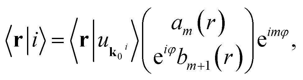
Therefore, by exploring the rotational invariance along the axis perpendicular to the graphene layer (z-axis), we set the general solutions of the Dirac-like Hamiltonian (1), in polar coordinates (r, φ), as two-component spinor states
 | (3) |
For a clear understanding of the variety of solutions, we decoupled this set of equations and rewrote them as two independent second-order differential equations in terms of the dimensionless universal variables ![[scr E, script letter E]](https://www.rsc.org/images/entities/char_e140.gif) = E/V0 and ρ = r/
= E/V0 and ρ = r/![[small script l]](https://www.rsc.org/images/entities/char_e146.gif) , where = vℏ/V0 sets a length normalization scale. Thus, the replacements am(r)[bm+1(r)] → Am(ρ)[Bm+1(ρ)] and the interface points (a, b, c) → (ρa = a/, ρb = c/, ρc = c/), lead to (for further details see ref. 12) the eigenvalue problem
, where = vℏ/V0 sets a length normalization scale. Thus, the replacements am(r)[bm+1(r)] → Am(ρ)[Bm+1(ρ)] and the interface points (a, b, c) → (ρa = a/, ρb = c/, ρc = c/), lead to (for further details see ref. 12) the eigenvalue problem
 | (4) |
− V(ρ)/V0)2 − γ2. A similar expression is obtained for the component Bm+1(ρ) by replacing m → m + 1 in (4).
In the following, we refer only to the energy eigenvalues, E, of the pseudo-relativistic states and will present the solutions for the analytical model and study the energy phase diagrams for GQDRs with the potential profile given by (see Fig. 1(b))
 | (5) |
3 Results and discussion
3.1 Full pseudo-relativistic confined state solutions
For the piecewise potential, the functions am(ρ) and bm+1(ρ) depend on the parameter β and on the relative value of the energy E with respect to the electrostatic potential amplitudes: V0, V1 and V2. Thus, by solving the determinant eigenvalue equation, we may set energy phase diagrams by varying the parameters β, the attractive (negative) voltages at the dot core and ring, V0 and V2, respectively, and the repulsive (positive) voltage within the barrier, V1, controlling the coupling between dot and ring systems. The solutions for Am(ρ) or Bm+1(ρ), defined in the open intervals (0, ρa), (ρa, ρb), (ρb, ρc) or ρ > ρc, can be written as
Am = C![[scr Z, script letter Z]](https://www.rsc.org/images/entities/char_e14b.gif) m(λρ), Bm+1 = C′m+1(λρ), m(λρ), Bm+1 = C′m+1(λρ),
| (6) |
m(z) is a linear combination of Bessel functions and with the constant C′ = −iλi/( − Vi/V0 + γ)C being determined by matching boundary conditions at the interfaces ρa, ρb and ρc along with the normalization of the spinor wavefunction, (3). The second-order differential equation requires the continuity of the spinor component| Am(ρ0−) = Am(ρ0+), | (7) |
![[scr V, script letter V]](https://www.rsc.org/images/entities/char_e149.gif) imposes discontinuity to the first derivatives, as deduced in ref. 12. As a consequence, the matching boundary conditions for the spinor component Bm+1 are analogous, after replacing Am ⇔ Bm+1 in (7).
imposes discontinuity to the first derivatives, as deduced in ref. 12. As a consequence, the matching boundary conditions for the spinor component Bm+1 are analogous, after replacing Am ⇔ Bm+1 in (7).
We consider the regions where the conditions λ12  0, λ22
  0, λ32
  0 and λ42 < 0 are fulfilled. Thus, the solutions of (4) are displayed in Table 2 with J|m|(z) and N|m|(z) (I|m|(z) and K|m|(z)) being the Bessel functions of the first and second kind (the modified Bessel functions of an imaginary argument), respectively. Using the conditions in eqn (6) and (7) and the relation C′ = −iλi/( − Vi/V0 + γ)C, we obtain a secular equation for the spinor components Am and Bm+1.
The voltage configuration applied on the metallic contacts can control the lateral confinement of carriers, thus changing the character of the solutions in the GQDR system. As displayed in Fig. 1(b), the piecewise profile defines four spatial regions and the reduced effective potential will be characterized locally by the following relative values: region 1 (GQD core), with V(r)/V0 = −1; region 2 (GQDR barrier), by V(r)/V0 = 1 ≡ V1/V0; region 3 (GQR rim), by V(r)/V0 = 2 ≡ |V2|/V0; and region 4 (external to the GQR), by V(r)/V0 = 0. The parameter i will be used to characterize every plausible configuration of relative potential strengths leading to QD and QR confinements. The solutions of (4) for Am (or equivalently, for Bm+1) are universal and independent of the sign of the dimensionless parameter γ, and assigned to states with antisymmetric pseudo-spins in the K and K′ valleys of the graphene Brillouin zone. However, the character of a typical pseudo-relativistic solution of (4) will depend on the sign of the normalized eigenvalue that defines the main character of states in each region and is given by λ12 = ( + 1)2 − γ2, λ22 = ( − 1)2 − γ2, λ32 = ( − 2)2 − γ2 and λ42 = 2 − γ2, for regions 1, 2, 3 and 4, respectively. The character of the solutions for signs of λi2 in the regions i = 1, 2, 3 and 4 are listed in Table 1 and becomes a general state character definition. Indeed, these solutions are extended into all regions along an arbitrary radial direction and can be combined into 16 classes of bound (oscillatory) and propagating or scattering states. However, given our present interest in the optical properties of this structure, we will be focusing, exclusively, on the 7 colored classes corresponding to bound states in different regions of the GQDR system. The chosen names refer to the larger probability density |ψ(r)|2 in the given region.
− V(ρ)/V0)2 − γ2 defines 24 characters of the solutions for the GQDR system. Only 7 are quasi-bond states, which are enlightened with colored columns for each corresponding class of confinement, and are labeled as: (class-II) dot–ring confinement (cyan), (class-VI) dot confinement (green), (class-VIII) barrier confinement (red), (class-X) dot–barrier–ring confinement (purple), (class-XI) ring confinement (dark gray), (class-XII) dot–barrier confinement (black) and (class-XIII) barrier–ring confinement (light gray). Class-III (yellow) defines a forbidden energy gap region with no oscillatory solution and the remaining white columns are classes of different wave-like states extended into the flat region, ρ > ρc, external to the GQDR (see Fig. 1)
 |
Unlike the previous work,12 we take into account the whole set of solutions for the GQDR system that can be classified as pseudo-relativistic confined states. In particular, we have considered, as the Dirac formalism admits, a linear combination of oscillatory functions, obtained for real values of λi, not only in the dot core and ring regions, but also in the barrier region. They can be sorted into two types of combined confinements: within the dot–barrier section (class-XII in Table 1) and in the barrier–ring region (class-XIII in Table 1).
3.2 Engineering bound state solutions
The energy phase diagrams yield a glimpse of the character modulation of the electronic state. By focusing on solutions listed in Table 2, it is possible to see that, for combinations of decaying functions (corresponding to confined states), the a-component solution Am(x) = CiIm(x) + CjKm(x) must be accompanied by the respective b-component solution Bm+1(x) = −DiIm+1(x) + DjKm+1(x) since the modified Dirac Hamiltonian in (1) couples the a and b components of the spinor state ψ(r, φ), where Di ∝ Ci. Therefore, the secular equation gives place to a 6 × 6 determinant, built from the continuity conditions of the eigenfunctions Am and Bm+1 at ρ = ρa, ρ = ρb and ρ = ρc.Following the character definitions in Table 2, one may map the classes of pseudo-relativistic GQDR states by changing the values of γ and i. Fig. 2 displays × γ diagrams for wave-like solutions within the GQDR system, identified by the same color codes as the classes of solutions listed in Table 1. When 1 = 0, electrons can be confined inside the dot and ring regions. More interestingly, the class-II solutions (cyan region) (Fig. 2(a)) correspond to pseudo-relativistic states localized simultaneously in the barrier and rim regions. For 1 > 0, two new regions emerge where class-VIII electrons are located in the barrier rim (red region) and class-X electrons within the dot–barrier–ring (purple region), as shown in Fig. 2(b). Note that the rhombic purple region (class-X) becomes the intersection between solutions linked to dot–ring (cyan) and barrier rim (red) bound states. If 2 < 1, two additional regions of bound states emerge simultaneously. They correspond to electrons confined in only the dot (green region) or in the dot–barrier rim and are depicted by the black region (class XII) in Fig. 2(c). Finally, if 2 > 1 (see Fig. 2(d)), another two new small regions appear corresponding to the conditions for electron confinement in the ring (dark gray region) and in the barrier–ring section (light gray). The tip of the triangular yellow region (class-III) framing the forbidden energies is defined by a critical value γc separating semiconductor and metallic regimes inherent to this structure. The gray dashed horizontal lines, in Fig. 2(c) and (d), define the Fermi level separating empty and occupied states in the structure. The vertical arrows indicate optical transitions that will be discussed later on when we will be studying the optical absorption of the GQDR system.
| m,i(x) |
λi2 < 0 | λi2 > 0 |
|---|---|---|
| m,i(x) |
λi2 < 0 | λi2 > 0 |
| m,2(x) |
C2Im,2(x) + C3Km,2(x) | C2Jm,2(x) + C3Nm,2(x) |
| m,3(x) |
C4Im,3(x) + C5Km,3(x) | C4Im,3(x) + C5Km,3(x) |
| m,4(x) |
C6Km,4(x) |
 | ||
| Fig. 2 × γ phase diagram for electrons for different combinations of barrier and ring voltages, respectively, V1 and V2 in the quantum dot–ring structure. Panel (a): V1 = 0 and V2 = −V0; panel (b): V1 = V0 and V2 = −V0; panel (c): V1 = 3V0/2 and V2 = −V0/4; panel (d): V1 = V0 and V2 = −3V0/2. Note that in panels (a) and (b), for fixed values of mass-term γ = 1 and energy = −0.5 (black points), the state character changes from the yellow class-III (forbidden energy value) to the red class-VIII (localized state in the barrier region 2) by increasing the barrier voltage, V1. The yellow and blue points in panels (c) and (d), represent the hole- and electron-eigenstates, respectively, at a fixed value of the quasi-mass term γ = 1.6 and GQDR spatial dimensions (ρa = 2, ρb = 5, and ρc = 9). γc is connected with the Fermi level in the system. | ||
When |V1| > V0 > |V2| (shallow ring), as depicted in Fig. 3(a), bound states can be formed in the barrier rim (red region), in the dot–barrier combined section (black region), in the dot–barrier–ring (purple region), in the ring (green region) and in the dot–ring (cyan region). Besides the energy phase-diagram, a few energy branches, n,0 × γ, are displayed in Fig. 3(a), calculated for the chosen potential profile with 1 = 1.5 and 2 = 0.25. In general, the existence of these bound states is guaranteed by the condition V1 ≠ 0. The probability density, |ψ(r)|2, of particular solutions are shown in Fig. 3(b), each column corresponding to a given value of γ = 0.5, 1.0, and 1.5 (indicated by vertical dashed lines in panel (a)). The corresponding energies are given at the crossing of these lines and the energy branches. The top-down order of the probability density plots corresponds to decreasing energies. Note, that by changing the energy for a fixed combination of parameters, the confinement character may be altered. This is evidenced in panel (b) for γ = 1.0, and will affect the optical transition oscillator strength. Due to the shallow ring voltage compared to the dot and barrier voltages we observe charge accumulation mainly in the dot, barrier, or dot–barrier rim elements, as shown by circular the white clouds in Fig. 3(b), for each different value of γ.
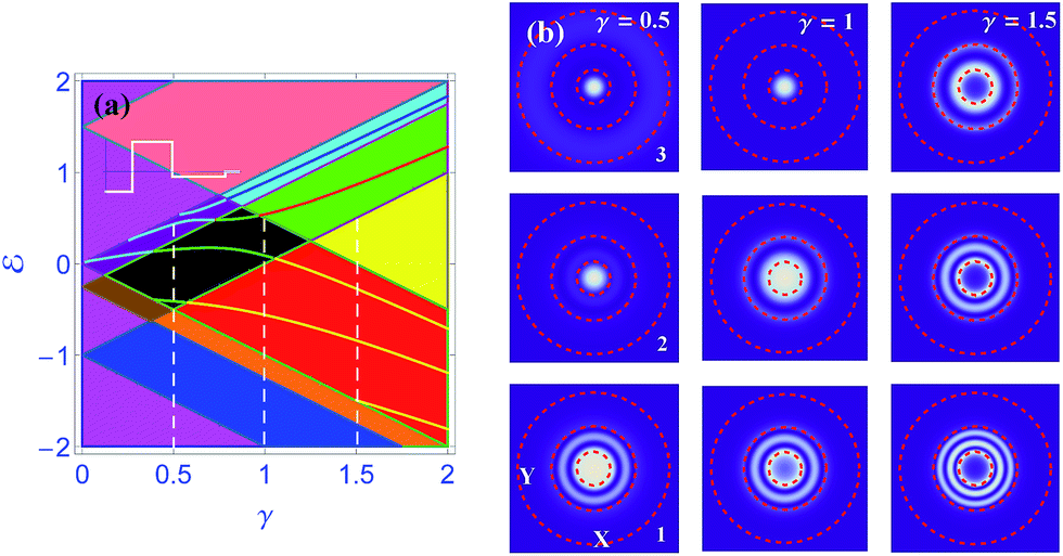 | ||
| Fig. 3 Panel (a): phase diagram × γ used for mapping the solutions belonging to classes II, VI, VIII, X, and XII of the GQDRs (ρa = 2, ρb = 5, and ρc = 9), for 1 = 1.5 and 2 = 0.25. The branches show the electron reduced energies, n,0, as a function of γ when Δρ = 3. Panel (b): planar X–Y probability densities for the first three energy states, calculated for γ = 0.5 (green branches in black region and cyan branch in purple region), 1 (yellow branch in red region, green branch in black region and red branch in green region) and 1.5 (yellow branches in red region). They are marked by vertical white dashed lines on the left and arranged in columns for increasing values of energy. The red dashed circles describe the isopotential borderlines of the GQDR system. | ||
A complementary scenario, with |V2| > |V1| > V0 (deep ring), has been displayed in Fig. 4(a). In this case, there are bound states in class-X (purple region) connected with classes XIII (light gray region) and II (cyan region). This new voltage profile has turned the black region (class-XII) occurring in Fig. 3(a), into a combination of a cyan section (class-II) and light gray region (class-XIII). Besides, a dark gray region (class-XI) has been introduced which stands for electron bound states within the ring structure. As expected, the mid-high value of the barrier rim allows the interaction between bound states in the dot (green region) and the ring (dark gray region). Thus, a part of the red region (class-VIII) has been turned into a light gray color class, with electrons confined preferably only in the dot–ring combined section due to its larger potential depth and barrier height values.
 | ||
| Fig. 4 Panel (a): × γ phase diagram showing the mapping of the solutions belonging to classes II, X, XI, XIII and VIII in the GQDR structure (ρa = 2, ρb = 3.6, and ρc = 7.6), for 1 = 2.5, 2 = 3. The branches are the electron reduced energies n,0 as a function of γ when Δρ = 1.6, for the different classes. Panel (b): planar X–Y probability densities for the first three energy states, (n = 0, 1, 2) for γ = 0.5(blue branches in purple region), 1 (orange branches in grey region) and 1.5 (orange branches in grey region). They are indicated by vertical white dashed lines and arranged in columns for increasing values of energy. | ||
The energy branches displayed in Fig. 4(a) correspond to the eigenvalues of n,0 as a function of the parameter γ for a given voltage configuration determined by |V2| > V1 > |V0|. In contrast to Fig. 3(b), the deeper ring voltage well compared to the dot and barrier voltages leads to charge accumulation outside the dot and barrier rim elements, as shown by the circular white clouds in Fig. 4(b), for various values of γ. In the scenario where |V2| > V1 > |V0|, it is possible to note an increasing number of states in Fig. 4(a) along the significant electron accumulation in the ring element, as seen in Fig. 4(b). As a consequence of the proximity between eigenvalues, we see the appearance of an anticrossing between the states of class-II (cyan) and class-X (purple). There are four other anticrossings in the rhombic class-XIII (light gray) region. Despite the close proximity between the eigenenergies, the mini-gaps persist in any potential configuration or with any γ values because of the shared symmetry between them that forbids the occurrence of degenerated states. The composition of the probability density panels in Fig. 4(b) is determined by the class-j region and the influence of the closer class-j ± 1. Then, it is expected that the probability density of state-1 (third row) will show the tendency to change from a spread distribution for γ = 0.5 within the ring, barrier and dot to another which is mainly located within the ring, as the one for γ = 1.5. To characterize these states, we can count the number of antinodes in the ring element. Notice that there are two, three, or four antinodes in ascending sort of states for the second column, where γ = 1. By following the energy branch of state in class-X (purple region), from γ = 0.5 to γ = 1, in class-XIII (light gray region), one can note the similarity between the probability density plots. This explains why state-1 in the third top row has less antinodes for γ = 0.5 as compared to γ = 1.5, since the corresponding energy eigenvalues are becoming more negative.
By increasing the separation Δρ between the dot and ring systems, more states with singular features appear confined in the barrier region (class-VIII in red) for γ = 1.5 and are being inserted from the continuum of states (class-IX), in a similar way as it happens for holes in the valence band within an inverted attractive potential. The energy eigenvalues as a function of increasing separation between the dot and ring elements of class-VIII solutions are depicted in Fig. 5(a). The branches show hyperbolic dispersions with growing density of energy states for increasing values of Δρ. This resembles the packing of holes near the bottom of a semiconductor quantum well with increasing well width. Here, the electrons confined to the inverted potential are coming from the extended states in the continuum below the bottom of the dot or ring regions. Another surprising characteristic that is observed is the probability distribution of electrons bound in the barrier. Unlike the solution for electrons confined in the dot or ring regions, the antinodes and nodes are inverted with respect to each other, in such a way that the electrons in the barrier, belonging to the class-VIII solution for the ground state, prefer to be located closer to the dot–barrier and barrier–ring interfaces, while showing a minimum probability distribution closer to the center of the barrier.
 | ||
| Fig. 5 Panel (a): the electron reduced energies, n,0, n = 1, …, 8, for states bound in the barrier region (class-VIII), as a function of reduced width Δρ and for 1 = 1.5 and 2 = 0.25 and for γ = 1.5 (see Fig. 2(c)). Panel (b): local probability density, |ψ(ρ)|2 of the first three energy branches, labeled as 1, 2 and 3 in panel (a), and calculated as a function of the width d, for the positions at the middle (ρ = ρa + Δρ/2, solid lines), dot–barrier left interface (ρ = ρa = 2, dashed lines) and barrier–ring right interface (ρ = ρb, dotted lines). This gives an indication of the number of antinodes and shows a preferential localization of states closer to the dot–barrier left interface. The panel of the right-hand side of (b) shows the respective probability density as a function of both ρ (horizontal) and Δρ (vertical). The white dashed lines indicate the dot–barrier and barrier–ring interfaces. The color scale indicates changes from maximum (red) to minimum (black) local probabilities. | ||
Fig. 5(b) shows the local probability density, |ψ(ρ)|2, of the first three bound states to the inverted barrier potential, labeled 1, 2 and 3 in Fig. 5(a), and calculated as a function of the width d, for the positions at the middle (ρ = ρa + Δρ/2, and show by red, blue and green solid lines), dot–barrier left interface (ρ = ρa, long dashed lines) and barrier–ring right interface (ρ = ρb, dotted lines). Note the number of antinodes and the preferential localization of states closer to the dot–barrier left interface. However, some peaks inside the barrier show the presence of electrons there for certain barrier values. For the first two excited states 2 and 3, the number of nodes increases to two and three, respectively, as can be seen in Fig. 5(b). Finally, the right panels show the probability density as a function of both ρ and Δρ. This is another way to map the distribution of carriers inside the barrier region. The white dashed lines in these panels indicate the dot–barrier and barrier–ring interfaces, highlighting the peculiar confinement effect at the junctions.
3.3 Optical response
The optical transitions in graphene nanostructures can be manipulated through combinations of graphene and substrate coupling and/or voltages applied to metallic gates since changes induced on confined states will affect the optical transition strengths. In this new panorama, we have carried out an exhaustive theoretical analysis of the optical absorption spectra of the GQDR structure displayed in Fig. 1. The interband optical transitions25 have been proven, showing different optical responses as gate voltages are varied. Here we have chosen a set of parameters (γ,i) in such a way that we can investigate the optical absorption active regimes of the GQDR device. We have already described the metallic regimes, in Fig. 3 and 4, for γ < γc whereas when γ > γc the yellow forbidden energy gap region emulates a semiconducting regime with an increasing energy gap for increasing values of γ. The interband transition processes described here involve the closest states around the Fermi level.
The forbidden states in the gap region (class-III) are defined by the constrictions,
 | (8) |
= 2γ − 1 − max(2, 1).
For the case of 2 < 1, we found a gap of Δ = 2γ − 1 − 1, as shown in Fig. 2(c), while the band offsets are Δe = 1 and Δh = 1, as indicated by the vertical black arrows. The sum of the energy differences, as usual for the massive Dirac fermions, is  . Furthermore, the active semiconductor region is defined by γ < γc with γc = (1 + 1)/2 and the Fermi energy F = (1 − 1)/2 > 0, as shown by the dashed horizontal line and measured from the top of the valence band. The vertical transitions are indicated by the gray solid line, connecting the state m = 0 in the barrier (red region or class-VIII) to m = 1 in the dot–ring (cyan region or class-II). In turn, for 2 > 1 in Fig. 2(d) we found a gap of Δ = 2γ − 1 − 2, while the band offsets are Δe = 2 and Δh = 1 as indicated by the black arrows. Here,
  , and the semiconducting regime is defined by γ < γc with γc = (1 + 2)/2 and the Fermi energy F = (2 − 2)/2 < 0 as shown by the dashed horizontal line. The vertical transitions for the potential profile in Fig. 4 occur from the top of the valence band state with one antinode m = 0 in the barrier (red region or class-VIII), towards several states of m = 1 in the dot–ring combined section (cyan region or class-II). This resembles a classic semiconductor with the promotion of electrons from the valence, leaving behind a hole, to occupy states in the conduction band.
Fig. 6 shows schematically typical optical absorption processes close to the Dirac point of the graphene Brillouin zone  in Fig. 6(a), and within the GQDR in Fig. 6(b). Direct optical transitions between the states below and above the Fermi level, F, are shown by vertical lines between the lower (j; j = −1) and upper (j; j = 1) states with massive Dirac fermionic dispersions. Hence 1 = c − F and −1 = −(v − F) with an energy gap of Δ = Δ(γ, 1, 2) for given GQDR parameters, γ, 1, 2. The conduction and valence band energies are measured from F, thus
|
c = 1 + Δ/2; v = −(−1 + Δ/2).
| (9) |
 | ||
Fig. 6 Typical optical transitions between hole and electron bound states near the Dirac point  in graphene (a) and in the GQDR structure (b). The absorbed photon has an energy of ħω ≈ 1 + −1 + Δ according to expressions in eqn (9). in graphene (a) and in the GQDR structure (b). The absorbed photon has an energy of ħω ≈ 1 + −1 + Δ according to expressions in eqn (9). | ||
To calculate the optical absorption, let us consider an elementary process in which an electron in a graphene monolayer is excited from the initial (|i〉) to a final (|f〉) state by absorption of a photon with energy ℏω. The incident light can be represented by the associated vector potential,
A(r,t) = A0![[small epsilon, Greek, circumflex]](https://www.rsc.org/images/entities/i_char_e107.gif) ![[thin space (1/6-em)]](https://www.rsc.org/images/entities/char_2009.gif) exp[i(k·r − ωt)] + c.c, exp[i(k·r − ωt)] + c.c,
| (10) |
is the polarization vector perpendicular to the light propagation and c.c stands for complex conjugate. The imaginary part of the complex dielectric constant is given by
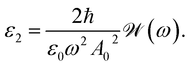 | (11) |
Here, ε0 is the vacuum dielectric constant and ![[scr W, script letter W]](https://www.rsc.org/images/entities/char_e536.gif) (ω) is the number of photons absorbed per unit area and per unit time, which is given, using a dipole approximation, by
(ω) is the number of photons absorbed per unit area and per unit time, which is given, using a dipole approximation, by
 | (12) |
![[scr F, script letter F]](https://www.rsc.org/images/entities/char_e141.gif) i and f are the respective initial and final electronic distribution functions for fermions at a given temperature, T. By using eqn (11) and (12), we can rewrite
i and f are the respective initial and final electronic distribution functions for fermions at a given temperature, T. By using eqn (11) and (12), we can rewrite
 | (13) |
 | (14) |
 for the subband (m, n).
The absorbed photon needs the energy ℏω ≈ 1 + −1 + Δ to trigger the transition between spinor states defined by the envelope functions that describe the motion of electrons in the conduction subbands (m, n), given by
 | (15) |
Subsequently, the evaluation of the matrix elements must be carried out in order to determine the strengths of the optical transitions, thus
 | (16) |
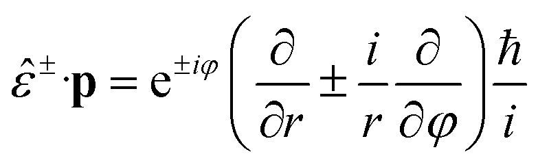
Hence, by exploring the graphene symmetry near the Dirac points k0 or k′0, for vertical transition we have k ≈ k0 implying u(f)k = u(i)k, and  . Therefore, by assuming the dipole approximation, when expanding 〈u(f)k|p|u(i)k〉, we have
| pfi = 〈u(f)k|p|u(i)k〉 = 〈uk0|p|uk0〉 + (k − k0)·∇kpfi(k0), | (17) |
|
〈ψf|·p|ψi〉 = ε·(k − k0)·∇kpfi(k0) + ε·〈ψf|p|ψi〉,
| (18) |
 | (19) |
 | (20) |
Finally, for right- and left-handed circularly polarized light (+ and −), we have
 | (21) |
After using reduced variables am(r)[bm+1(r)] → Am(ρ), [Bm+1(ρ)], we obtain
 | (22) |
 . According to Bessel function recurrence relations, the follow conditionals must be accomplished,
 | (23) |
Since the imaginary part of the dielectric constant is proportional to the optical absorption then, for the GQDR, we find
 | (24) |
with  .
.
For a realistic simulation of the optical response, the choice of parameters has been based on values experimentally reported in the literature. In ref. 2, epitaxially grown graphene on a SiC substrate has been characterized displaying a gap of ≈0.26 eV, with a reported graphene–substrate interaction of β = 130 meV. Other parameters are band width (t = 2.7 eV) and carbon–carbon distance (a0 = 0.142 nm). Moreover and according to the tight binding model,  . For a radius of R = 25a0 ≈ 3.55 nm we obtain a dot voltage gate of 0 = ℏv/R = 3t/50 ≈ 162 meV. Thus, the dimensionless graphene–substrate strength is γ = β/0 = 130/162 ≈ 0.8. Hence, we get the scaling factor that determines the energy interval by the equivalence between −0.8 < < 0.8 and −130 meV < E < 130 meV. In the same way, for R = 50a0 ≈ 7.1 nm we have 0 = ℏv/R = 3t/100 ≈ 81 meV. Thus the dimensionless graphene–substrate strength is γ = β/0 = 130/81 ≈ 1.6. In this case, the equivalent energy ranges are −1.6 < < 1.6 and −130 meV < E < 130 meV. These last values were used in the optical absorption calculations.
First, we use the potential profile displayed in Fig. 2(d) where we have fixed the ring gate voltage (2 = 1.5) and calculate the hole and electron class-II (cyan region) and class-XI (dark gray region) energy values, n,0 as a function of barrier gate voltage 1 in the graphene dot–ring structure, as shown in Fig. 7(a), for the structural parameters just described. Transitions connecting states from class-VIII (red region), in the barrier, to class-XI (dark gray), in the ring, or to class-II (cyan region) states, in the dot–ring combined section, are indicated by the vertical lines A and B, respectively. Fig. 7(b) displays the dependence of the full optical absorption spectrum, α(ω, T), for temperatures T1 = 4 K (green lines) and T2 = 300 K (yellow lines), as the incident photon energy is increased. Notice that there are four different regions, distinguished by four colors. Except for in the yellow region, the bound states are observed. As mentioned before, the bound states are classified by the larger probability density. For instance, the electronic states lying in the red-, dark gray- and cyan-regions are mainly localized in the barrier, ring, and dot and ring combined areas, respectively. In addition, the energy spectrum is modulated by increasing 1, but with a different rate variation. More specially, the energy of the states lying in either the dark gray- or cyan-regions is only slightly changed. The energy spectra of the states in the red region, however, are considerably increased. Besides, the number of bound states in the red region also increases with increasing 1. This behavior can be attributed to an increase in the number of bound states in the anti-dot due to an increase of quantum confinement. Hence, in the regime of small 1, there are four different regions. In contrast, in the regime of large 1, only three regions remains. To understand the influence of barrier gate voltage on the energy spectrum and on electronic probability distribution, we compute the absorption spectra related to the transitions from the states lying in the red region to the dark gray- and cyan-regions, for several values of 1, and at T = 4 and T = 300 K, respectively, as shown in Fig. 7(b). For clarity, the corresponding transitions are schematically indicated by vertical arrows A and B, as shown in Fig. 7(a). Notice that for a small value of 1, such as 1 = 0.3, only four peaks are observed. In addition, the peak with the highest energy shows the strongest intensity. This can be attributed to the larger overlap integral between the state located in the barrier and the one lying in the dot and ring areas in comparison with its counterpart associated with the transitions between the states strongly localized in the barrier and in the ring regions.
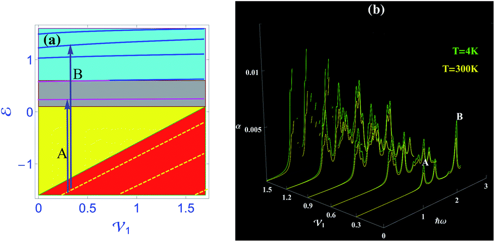 | ||
| Fig. 7 (a) Reduced energies m,0 of holes (dashed-lines) and electrons (solid-lines) in the graphene dot–ring structure as a function of barrier gate voltage 1. (b) Absorption spectra for right-handed circular polarization, for different barrier gate voltages 1 at temperature T = 4 K (green solid line) and T = 300 K (yellow solid line). The peaks A and B in panel (b) are associated with the transitions (1, 0) ↦ (1, 1) and (1, 0) ↦ (4, 1), respectively, as demonstrated by vertical arrows A and B in panel (a). The following parameters were used in the calculation: ρa = 2, ρb = 5, ρc = 9, 2 = 1.5 and mass-term γ = 1.6. | ||
With increasing 1, several new features emerge. For instance, the number of peaks increases and the peak with the highest intensity shifts to the lower energy side of the spectrum. Furthermore, the intensity of the peaks at T = 4 K becomes stronger and is stronger than for the corresponding peaks at T = 300 K. These observations give further support for the tunability of the energy spectrum by applied voltages 1. The underlying physics can be understood in the following way. An increase in the number of bound states in the red region gives rise to more peaks in the spectrum. As 1 increases, the transition energy decreases, and thus, the effect of temperature becomes more and more significant. As a result, the transition probability for lower transition energy is increased. Hence the intensity of the peaks at the lower energy side becomes enhanced. On the another hand, an increase in the occupation probability of states lying in the dark gray region, as determined by the Fermi–Dirac distribution function, leads to a reduced transition probability as the temperature increases. Owing to the reduced transition energy, this effect turns out to be more efficient in the case of larger 1 values. Therefore, the intensity of the peaks at T = 4 K is much more enhanced than for those at T = 300 K.
Next, we used the profile of Fig. 2(c) where we have fixed the barrier gate voltage (1 = 1.5) and calculate the class-VII hole and class-II (cyan region), class-VI (green region) and class-XI (dark gray region) electron energy states, m,0 for the same set of parameters, as a function of the ring gate voltage 2 in the graphene dot–ring structure, as shown in Fig. 8(a). Transitions connecting states from class-VIII (red region), in the barrier, to class-II (cyan region) states, in the dot–ring section, are indicated by vertical lines A and B, respectively. Fig. 8(b) displays the dependence of the full optical absorption spectrum, α(ω, T), for temperatures T = 4 K (green lines) and T = 300 K (yellow lines), as the incident photon energy is increased. As the ring-voltage increases, the number of peaks increases accompanied by a shift of the corresponding peaks to the low energy side. Besides, the intensity of the absorption peaks initially increases. It reaches a maximum at 2 = 0.9 and, after that, the intensity starts to decrease. Besides, the intensity of the peak B is always stronger than that of peak A. At large 2, the temperature effect turns out to be more dominant and the underlying physics is as follows. As the 2 increases, the energy of the bound states decreases, but the decreasing rate for the states in either the cyan- or dark gray-regions is larger than that for the states in the red-zone. Then there are more bound states entering the energy interval (−1.5 to 1.5) than states leaving this energy interval. Hence the number of peaks increases and overall absorption spectrum shifts to the lower energy side. In addition, the reduced transition energy leads to an enhanced intensity of the corresponding peak transitions. Thus initially, the intensity of the absorption spectrum increases. On the other hand, the intensity of the absorption spectrum depends strongly on the overlap between the initial state, which is mainly distributed in the barrier region, and the final state. When 2 < 0.9, the electron lying in the final state is confined in the both dot and ring regions. Since the 2 attracts electrons, it drives them to escape from the dot area and move into the ring region. Thus the electronic transition probability decreases in the former while it increases in the latter case. At a critical point of 2 = 0.9, the transition from class II to class XI for the lowest final state takes place. After that, the electron is no longer confined in the dot region but, instead it becomes mainly confined in the ring region. Therefore, the overlap integral between states reduces, leading to a reduction in the intensity of the peaks in the absorption spectrum.
 | ||
| Fig. 8 (a) Reduced energies m,0 of holes (dashed-lines) and electrons (solid-lines) in the graphene dot–ring structure as a function of ring gate voltage 2. (b) Absorption spectra for right handed circular polarization for different ring voltages 2 at temperature T = 4 K (green solid line) and T = 300 K (yellow solid line). The peaks A and B in (b) are associated with the transitions (1, 0) ↦ (1, 1) and (2, 0) ↦ (1, 1), respectively, as demonstrated by vertical arrows A and B in (a). The following parameters were used in this calculation: ρa = 2, ρb = 5, ρc = 9, 1 = 1.5 and mass term γ = 1.6. | ||
In order to thoroughly understand the barrier-voltage tuning energy spectra process as well as the optical absorption, we constructed the (m,0, 1) phase diagram of the GQDR with ρa = 2, ρb = 5, ρc = 9, 2 = 1.5 and γ = 1, in the intervals 1 < 1 < 2.5 and −1 < m,0 < 1, as shown in Fig. 9(a). Notice that there are four bound states in a metallic regime. As 1 increases from 1 to 2.5, both the energies as well as the characteristics of these states change, as indicated by the color code of the region in which they are located. Furthermore, three anticrossings between energy branches emerge successively. The mechanism of the barrier-voltage tuned energy spectrum is the same as discussed in Fig. 7. The manifestation of these anticrossings in the optical absorption spectrum and its barrier-voltage tunability, for three typical transitions: (0, 1) ↦ (1, 2), (1, 2) ↦ (2, 3) and (2, 3) ↦ (3, 4), are shown in Fig. 9(b) where the transition energies and oscillator strengths are plotted and where the values are represented by the size of the circles. To guide the eyes, the corresponding transitions are indicated by color arrows in Fig. 9(a). One notices that the transition energy, for these three kinds of optical transitions, exhibits an oscillatory behavior due to the anticrossings, with the minimum transition energy in the place where the anticrossing occurs. As the 1 increases, the characteristics of states involved in the transition change, leading to a variation in the overlap integral between the initial and final states. Hence, the oscillator strength changes accordingly. The anticrossing induced by the mixing of the involved states also induces variations in the oscillator strength, due to the strong coupling between the initial and final states near the anticrossing regions, which contributes to the variation of the overlap integral. Therefore, the optical spectrum can be modulated considerably by the applied voltage 1.
 | ||
| Fig. 9 (a) Reduced energies m,0 of a particle in the graphene dot–ring structure as a function of barrier gate voltage 1. The green arrow indicates (0, 1) ↦ (1, 2) transition, while the blue and red arrows illustrate (1, 2) ↦ (2, 3) and (2, 3) ↦ (3, 4) transitions. (b) Optical transition energies corresponding to the transitions are indicated by colorful arrows in panel (a) as a function of 1. Here the same color scheme is used and the circle radii are proportional to the corresponding oscillator strengths for right-handed circular polarization. The following parameters were used in this calculation: ρa = 2, ρb = 5, ρc = 9, 2 = 1.5 and γ = 1. | ||
4 Conclusions
In summary, we have studied the formation of pseudo-relativistic Dirac states in GQDR gated structures of graphene monolayers over a substrate. The graphene–substrate interaction induces a tunable energy gap at the Dirac points of the graphene Brillouin zone with a critical value of γc separating metallic from semiconductor regimes in the same sample, as seen for two main potential profile configurations (|V1| > V0 > |V2| and |V2| > |V1| > V0). Our formalism based on the energy phase diagram allowed us to calculate, compose and organize a full set of Dirac bound states in a combined system, resulting from a variety of mixed pure states in the different structure regions: the dot, the barrier and the ring, with their character defined according to the large density of probability in each spatial region. These states can be manipulated and their symmetry character changes drastically according to the ratio between relative gate voltages,1 and 2. Remarkable electronic properties emerge, as an effective breaking of the particle–hole symmetry, with the inclusion of a degree of freedom through the barrier region between the dot and the ring structures, gives place to a rich band structure, that goes from the well spaced hyperbolic energy branches in a single QD to a set of convoluted energy states with anticrossing regions, in GQDR system. The energy branches become as close to each other as the increase on the bias gate allows them to but always keep minigaps between them. Hence, this behaviour is assured from the linearity inherent in the Dirac equation that avoids degeneracies in the eigenstate solutions. It is worth to mention the occurrence of peaks of charged carriers localized near the dot–barrier and barrier–ring interfaces and even more, the nonzero probability density in the middle of the barrier region.
Interband infrared transition processes from the top valence band to the bottom conduction band states, take place close to the Fermi level. The optical absorption spectra as a function of the structural parameters have a peculiar behavior in contrast to the non-relativistic quantum systems. By fixing the quantum dot voltage and varying the barrier and/or rim voltages, we may form a variety of pseudo-relativistic states with unusual optical properties. This graphene based quantum dot–ring device, resembling a classic semiconductor with a variable energy gap tuned externally, can be explored for infrared optoelectronic devices.
Acknowledgements
The authors thank Carlos Trallero-Giner for very insightful and fruitful discussions. We gratefully acknowledge the financial support from SECITI-DF/CLAF and the Brazilian Agencies, MCT/CNPq, CNPq, CAPES and FAPESP grant 2014/02112-3 (VLR).References
- F. Schwierz, Nat. Nanotechnol., 2010, 5, 487–496 CrossRef CAS PubMed.
- B. J. Kim, S. H. Um, W. C. Song, Y. H. Kim, M. S. Kang and J. H. Cho, Nano Lett., 2014, 14, 2610–2616 CrossRef CAS PubMed.
- R. Maurand, P. Rickhaus, P. Makk, S. Hess, E. Tóvári, C. Handschin, M. Weiss and C. Schönenberger, Carbon, 2014, 79, 486–492 CrossRef CAS.
- F. Wang, Y. Zhang, C. Tian, C. Girit, A. Zettl, M. Crommie and Y. R. Shen, Science, 2008, 320, 206–209 CrossRef CAS PubMed.
- J. R. Williams, T. Low, M. S. Lundstrom and C. M. Marcus, Nat. Nanotechnol., 2011, 6, 222–225 CrossRef CAS PubMed.
- A. H. C. Neto, F. Guinea, N. M. R. Peres, K. S. Novoselov and A. K. Geim, Rev. Mod. Phys., 2009, 81, 109–162 CrossRef.
- A. K. Geim, Science, 2009, 324, 1530–1534 CrossRef CAS PubMed.
- Y. Sun, S. Wang, C. Li, P. Luo, L. Tao, Y. Wei and G. Shi, Phys. Chem. Chem. Phys., 2013, 15, 9907 RSC.
- P. K. Herring, A. L. Hsu, N. M. Gabor, Y. C. Shin, J. Kong, T. Palacios and P. Jarillo-Herrero, Nano Lett., 2014, 14, 901–907 CrossRef CAS PubMed.
- B. Zhao, J. M. Zhao and Z. M. Zhang, Appl. Phys. Lett., 2014, 105, 031905 CrossRef.
- K. Matsumoto, K. Maehashi, Y. Ohno and K. Inoue, J. Phys. D: Appl. Phys., 2014, 47, 094005 CrossRef.
- L. Villegas-Lelovsky, C. Trallero-Giner, V. Lopez-Richard, G. E. Marques, C. E. P. Villegas and M. R. S. Tavares, Nanotechnology, 2012, 23, 385201 CrossRef PubMed.
- P. Recher, J. Nilsson, G. Burkard and B. Trauzettel, Phys. Rev. B: Condens. Matter Mater. Phys., 2009, 79, 85407 CrossRef.
- S. Y. Zhou, G.-H. Gweon, A. V. Fedorov, P. N. First, W. A. D. Heer, D.-H. Lee, F. Guinea, A. H. C. Neto and A. Lanzara, Nat. Mater., 2007, 6, 770–775 CrossRef CAS PubMed.
- C. Enderlein, Y. S. Kim, A. Bostwick, E. Rotenberg and K. Horn, New J. Phys., 2010, 12, 033014 CrossRef.
- J. P. Hague, Phys. Rev. B: Condens. Matter Mater. Phys., 2011, 84, 155438 CrossRef.
- G. Giovannetti, P. A. Khomyakov, G. Brocks, P. J. Kelly and J. V. D. Brink, Phys. Rev. B: Condens. Matter Mater. Phys., 2007, 76, 073103 CrossRef.
- T. Luo, A. P. Iyengar, H. A. Fertig and L. Brey, Phys. Rev. B: Condens. Matter Mater. Phys., 2009, 80, 165310 CrossRef.
- A. R. Akhmerov and C. W. J. Beenakker, Phys. Rev. B: Condens. Matter Mater. Phys., 2008, 77, 085423 CrossRef.
- L. Villegas-Lelovsky, A. C. Dias, R. Gargano and F. Qu, EPL, 2015, 111, 38002 CrossRef.
- P. G. Silvestrov and K. B. Efetov, Phys. Rev. Lett., 2007, 98, 016802 CrossRef CAS PubMed.
- P. Hewageegana and V. Apalkov, Phys. Rev. B: Condens. Matter Mater. Phys., 2008, 77, 245426 CrossRef.
- D. A. Bahamon, A. L. C. Pereira and P. A. Schulz, Phys. Rev. B: Condens. Matter Mater. Phys., 2009, 79, 125414 CrossRef.
- M. Zarenia, J. M. Pereira, A. Chaves, F. M. Peeters and G. A. Farias, Phys. Rev. B: Condens. Matter Mater. Phys., 2010, 81, 045431 CrossRef.
- L. Yang, J. Deslippe, C.-H. Park, M. L. Cohen and S. G. Louie, Phys. Rev. Lett., 2009, 103, 186802 CrossRef PubMed.
| This journal is © The Royal Society of Chemistry 2016 |